Design of a Step-Down DC-DC Controller Integrated Circuit
with Adaptive Dead-Time Control
by
Zhipeng Li
S.B. EE, M.I.T., 2009; S.B. Physics, M.I.T., 2009
Submitted to the Department of Electrical Engineering and Computer Science in Partial Fulfillment of the Requirements for the Degree of
Master of Engineering in Electrical Engineering and Computer Science
ARCHIVES
at the Massachusetts Institute of TechnologyMASSACHUSETTS NST1 3 ITIUTEF
May 2010
---@2010
Massachusetts Institute of TechnologyA09
2
All rights reserved.
L
BRAR E
Author... ... ... ...
Department of Electrical Engineering and Computer Science May 21, 2010
Certified by... ... ... ...
Eric Gu Design Engineer, Linear Technology Corporation VI-A Company Thesis Supervisor
C ertified by... ... j... ...
David Perreault
Associate Professor M.I.T. Thesis Supervisor
A ccep ed by ... ... ... .. ... . . .
Accepted by...
Dr. Christopher J. Terman Chairman, Department Committee on Graduate Theses
Design of a Step-Down DC-DC Controller Integrated Circuit with
Adaptive Dead-Time Control
by
Zhipeng Li
Submitted to the
Department of Electrical Engineering and Computer Science May 21, 2010
In Partial Fulfillment of the Requirements for the Degree of Master of Engineering in Electrical Engineering and Computer Science
Abstract
A constant-frequency peak current mode synchronous step-down DC-DC controller
inte-grated circuit has been designed with adaptive dead-time control. The adaptive dead-time control circuitry is implemented as digital delay-locked loop with digital counters as mem-ory elements. In periodic steady state, the switch is controlled to turn on exactly when the body diode starts to conduct current. The conduction loss through MOSFET switch body diode is minimized. In spice simulation, this scheme increases the overall efficiency in low-voltage applications by up to 3%.
VI-A Thesis Supervisor: Eric Gu
Title: Design Engineer, Linear Technology Corporation Thesis Supervisor: David Perreault
Acknowledgments
I would like to thank Eric Gu, my VI-A company thesis supervisor, for proposing the idea behind this thesis. He served as a great mentor. He was always ready to answer my questions and provide his technical expertise. I learned a great deal from him in the area of circuit design.
I would like to thank Professor David Perreault for supervising this thesis. He gave
many insightful technical comments to my thesis proposal and this thesis. His generous support is much appreciated.
There are many other individuals that served as valuable sources of information at Linear Technology that I would like to thank too. This thesis would not be possible without the support from Linear Technology. This work would not have been fabricated into real silicon without the excellent work of Lei Zhang and Lucy Lu on circuit layout.
I would also like to thank all my family and friends that have supported throughout my life. I extend my biggest thanks to my parents, who have served as source of inspirations throughout my life.
Contents
1 Introduction 15
1.1 Converter Efficiency . . . . 15
1.2 Double Data Rate Memory Termination . . . . 16
1.3 Chip Specification . . . . 20
1.4 Thesis Overview . . . . 20
2 System Overview 23 2.1 From Linear Regulator to Switching Regulator . . . . 23
2.2 Synchronous Step-down Converter . . . . 25
2.3 Control Scheme . . . . 26
2.3.1 Voltage Mode Control . . . . 26
2.3.2 Current Mode Control . . . . 26
2.3.3 Compensation . . . . 27
3 Dead Time Control 33 3.1 Dead-Time Control . . . . 33
3.2 Estimation of Efficiency Improvement.. . . . . . . . . 34
3.3 Prior Art and Other Control Schemes . . . . 35
3.4 Control Scheme with Digital Delay-Locked Loop . . . . 38
4 Chip Design 45 4.1 O verview . . . . 45
4.2 Internal Supply, Biasing, and Clock . . . . 4.3 Configuration Selection . . . .
4.4 Error Amplifier . . . . 4.5 Current Comparator . . . . 4.5.1 Current Threshold . . . . 4.5.2 Wide Input-Range Current Comparator 4.6 Adaptive Dead-Time Controller . . . .
4.6.1 Signal Sensing . . . . 4.6.2 Latch . . . . 4.6.3 Up-Down Counter . . . . 4.6.4 Delay Line . . . . . . . . 45 . . . . 47 . . . . 50 . . . . 5 1 . . . . 5 1 . . . . 52 . . . . 53 . . . . 53 . . . . 56 . . . . 59 . . . . 62 5 Full-Chip Simulation
5.1 Simulations of Test Mode . . . .
5.2 Simulations of Switching Mode . . . .
6 Conclusion and Future Work
6.1 C onclusion . . . . 6.2 Known Issues and Discussion . . . .
List of Figures
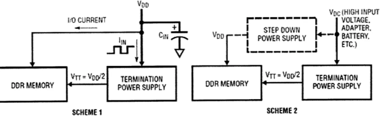
1-1 Two basic design schemes for DDR termination power supplies . . . . 17
1-2 High efficiency DDR memory termination power supply with VTT = VDD/ 2 18 1-3 High efficiency DC-DC converter with high step-down conversion from 15V to 1.8V . . . .. . . . 19
2-1 Linear regulator: concept and implementation . . . . 23
2-2 Step-down DC-DC converter . . . .. . . . 24
2-3 Buck converter with free-wheeling diode.. . . . . 25
2-4 Synchronous buck converter . . . . 25
2-5 Feedback signals: when a current mode control scheme is used, the current feedback is required . . . . 27
2-6 Simplified block diagram of an uncompensated current-mode switching reg-ulator . . . . 27
2-7 Block-level schematics of an open-loop current-mode regulator . . . . 28
2-8 Simplified block diagram of an compensated current-mode regulator . . . . 28
2-9 Asymptotic bode plot of loop dynamics. . . . . 29
2-10 Spice simulated Bode plots of the uncompensated (top) and compensated (bottom ) system s . . . . 31
3-1 Synchronous buck converter . . . . 33
3-2 Fixed delays used to prevent shoot-through . . . . 36
3-4 The delay-lock loop to align SBSW and SBBG signals (parts of this circuitry
are shown later in Chapter 4 in more details) . . . . 39
3-5 BG-off to TG-on edge . . . .. 41
3-6 The delay-lock loop to align SBSW and SBTG signals (parts of this circuitry are shown later in Chapter 4 in more details) . . . . 41
3-7 Both edges . . . . 43
4-1 Simplified Block Diagram . . . . 46
4-2 If CSELB is high, VREFIN is divided by half before applied to the positive input of error amplifier . . . . 48
4-3 If CSEL is grounded, VREFIN is divided by half before applied to the positive input of error amplifier . . . . 49
4-4 Error amplifier design . . . . 50
4-5 Current sense threshold versus VITH in this design . . . . 52
4-6 OUT is high if SW rises 200mV above TD, or 200mV below SGND . . . . 55
4-7 Latch determines which of two falling edges, SB1 and SB2, comes first after each rising RESET pulse . . . . 57
4-8 Timing of Edges. From top to bottom, the signals are: ITRP, current comparator output and the reset signal for latches; DOWN, logic signal for counter down transition; UP, logic signal for counter up transition; BG, the gate voltage of bottom power switch; SBBG, logic signal that is low if the gate voltage of bottom switch is higher than the MOSFET threshold voltage (1.6V); SW, the SW node voltage; SBSW, logic signal that is low if the SW node is more than 200mV below ground. . . . . 58
4-9 If T=0 at rising edge of CLK,
Q
does not change after the negative edge of CLK; if T=1 at the falling edge of CLK,Q
changes to QB after the negative edge of CLK . . . . 604-10 4-bit Counter . . . . 61
4-11 The delay line. . . . . . . . 62
List of Tables
1.1 Specification of the proposed step-down controller . . . . 20
5.1 Simulated Current Threshold . . . . 66 5.2 Simulated Efficiency with FIXDT connected to INTVCC or SGND . . . . . 68
Chapter 1
Introduction
1.1
Converter Efficiency
DC-DC converters are a category of electronic circuits designed to efficiently convert a
source of direct current (DC) from one voltage level to another.
Many electronic devices, such as cellular phones and laptop computers, contain multiple circuit blocks; each circuit block may have its own supply voltage level requirement, different from the one supplied by the battery or an wall adapter. To increase efficiency and extend battery lifetime, we need efficient ways to convert DC voltage sources to different levels. Over the years, technology has moved from linear regulator to switching regulator, from asynchronous converter to synchronous converter. The architectural changes have led to significant increases in converter efficiency.
To push even further, every tiny bit of efficiency loss is targeted for reduction. In this thesis, we look at how to increase efficiency of a synchronous DC-DC converter further by
adaptively controlling the dead-times.
The synchronous DC-DC converter has higher efficiency because its lower conduction loss compared to asynchronous converter with free-wheeling diodes. The synchronous con-verter includes a pair of power MOSFET switches. The switches are repeatedly switched on and off complementarily by a control signal from the controller. Dead-times are the short period of time when both gate drive signals are off. During this period of transition,
the body diode on one of the switches turns on, storing charge during the dead time and requiring a reverse recovery period. If the dead-time is too short or ever goes negative, huge amount of current could flow through the two power MOSFET from the input voltage source to ground. On the other hand, if the dead-time is too long, conduction loss is large. Because of the load variation and the internal timing delays presented both in the control
IC and power MOSFETs due to process variation, in previous controllers, the dead times
are often made large and fixed internally. The conduction through body diode during the dead time therefore presents a significant efficiency loss. On the proposed controller, an adaptive dead-time control block is integrated to minimize this conduction time through
MOSFET switch body diode. We expect this effort to increase efficiency by up to 3% in
the low-voltage applications.
1.2
Double Data Rate Memory Termination
One important low-voltage high-current application of a DC-DC converter is termination power supply for the Double Data Rate (DDR) Synchronous Dynamic Random Access Memory. We design this high-efficiency controller to be easily configurable for the DDR memory termination and for the general-purpose applications.
The DDR memory transfers data on both the rising and falling edges of the clock cycle, thus doubling the effective transfer rate of the Single Data Rates Synchronous Dynamic Random Access Memory (SDR SDRAM). However, a typical DDR memory system needs an additional power supply for its termination. The termination power supply (VTT) must
track the I/O Power supply (VDD) with VTT = VDD/2 to ensure good signal quality. Further, the VTT power supply must be able to both source and sink current.
There are two basic design schemes for DDR memory power supply termination [4] as shown in Fig. 1-1. In scheme 1, VTT is directly generated from the VDD rail. This
scheme has been very popular in low power (< 10A) DDR applications. However, for high power application, this scheme has a few disadvantages. The VDD supply must be able to
provide enough current to power both VTT circuit and the I/O current of the DDR memory.
V ,-(HIGH INPUT
11"" CUR""" """"T " " VOLTAGE.
+I STEP 0OWN
l
ADAPTEI00 4 POWER SUPPLY " T ATR
r
VV 2 TERMINATION VTT = VD2 TERMINATION
DDR MEMORY POWER SUPPLY DDR MEMORY POWER SUPPLY
SCHEME1 SCHEME 2
Figure 1-1: Two basic design schemes for DDR termination power supplies
low impedance to minimize the VDD rail switching noise. These capacitors significantly increase board size and cost. Scheme 2 is preferred for high power applications, where VTT is generated from higher input voltage sources.
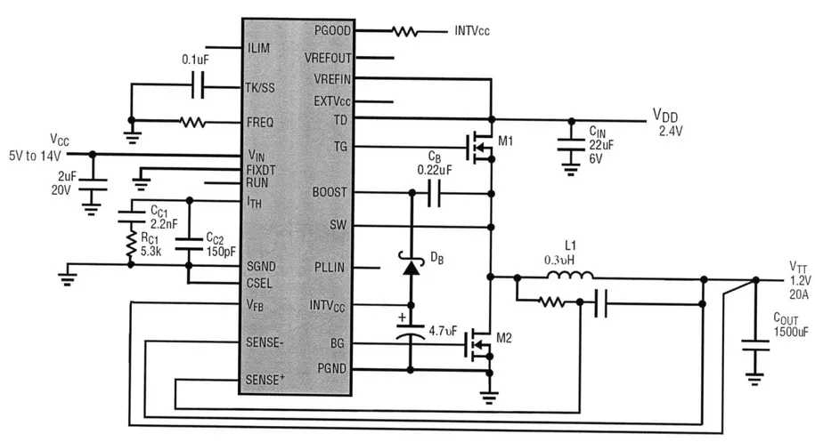
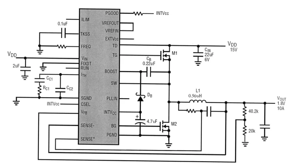
The controller designed in this thesis will satisfy these DDR requirements, and it can be used in both schemes. For Scheme 1, the Configuration Selection pin CSEL is shorted to ground, the reference voltage pin VREFIN will be connected to the input source and the applied voltage gets divided by half internally as the error amplifier reference voltage, as shown in Fig. 1-2. For Scheme 2, VREFIN pin is connected to an external precision reference. For a general purpose DC-DC converter, VREFOUT, where the internal Bandgap voltage is buffered, is connected to VREFIN, and CSEL is shorted to the 5V supply INTVCC, the output voltage can be programmed by a resistor divider, as shown in Fig. 1-3.
VCC 5V to 14V -VTT - 1.2V 20A COUT 1500uF
Figure 1-3: High efficiency DC-DC converter with high step-down conversion from 15V to 1.8V
VDD
VOUT
1.8V
1.3
Chip Specification
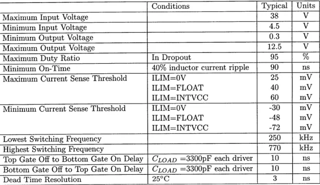
The proposed controller can be configured for DDR memory termination as well as a general-purpose DC-DC converter. An adaptive dead-time control (ADTC) scheme is implemented to reduce the conduction loss due to the power MOSFET body diode turn-on. The proposed controller integrated circuit (IC) will minimize the dead-times to typical 10 nanoseconds. In the application for DDR memory termination, it should be able to drive devices capable to sink and source up to 20 amperes of current. Additionally, its output should be able to go down to 0.3V. These specifications is summarized in Table 1.1. For a complete description of pin functions on this proposed integrated circuit, please refer to Appendix A.
Conditions Typical Units
Maximum Input Voltage 38 V
Minimum Input Voltage 4.5 V
Minimum Output Voltage 0.3 V
Maximum Output Voltage 12.5 V
Maximum Duty Ratio In Dropout 95 %
Minimum On-Time 40% inductor current ripple 90 ns
Maximum Current Sense Threshold ILIM=OV 25 mV
ILIM=FLOAT 40 mV
ILIM=INTVCC 60 mV
Minimum Current Sense Threshold ILIM=OV -30 mV
ILIM=FLOAT -48 mV
ILIM=INTVCC -72 mV
Lowest Switching Frequency 250 kHz
Highest Switching Frequency 770 kHz
Top Gate Off to Bottom Gate On Delay CLOAD =3300pF each driver 10 ns Bottom Gate Off to Top Gate On Delay CLOAD =3300pF each driver 10 ns
Dead Time Resolution 250C 3 ns
Table 1.1: Specification of the proposed step-down controller
1.4
Thesis Overview
Chapter 2 covers the basics of the buck switching regulator operation, control and compen-sation. The adaptive dead-time control scheme is described in Chapter 3. The design of each sub-circuit of this proposed DC-DC controller is detailed in Chapter 4, and
simula-tion results are described in Chapter 5. Finally, the issues discussed in the thesis will be summarized and future works are suggested in Chapter 6.
Chapter 2
System Overview
This chapter describes the basic operation of the step-down switching regulator IC. It then outlines the control schemes used.
2.1
From Linear Regulator to Switching Regulator
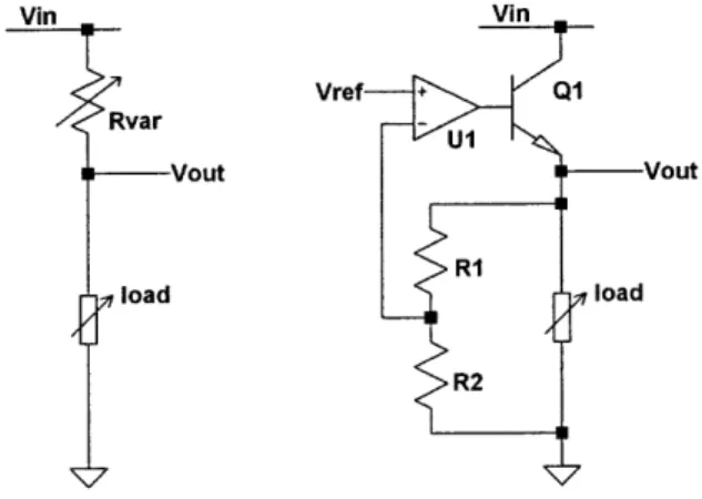
The simplest way to convert a high and varying input DC voltage to a lower but constant output voltage is a dynamically controlled voltage divider circuit - a linear regulator. As shown in Fig. 2-1, by dynamically adjusting the upper resistor of the voltage divider, one can achieve a fixed constant voltage at output despite the disturbances on the input and load. Vin Vin Vref + Qi Rvar -Vout Vout R1 load load R2
The drawback of the linear regulator is its low efficiency. Power is wasted on the variable resistor (the transistor Q1 in Fig2-1). The efficiency of a linear regulator, to the first order,
is VOUT/VIN. When VIN and VOUT are further apart, a linear regulator is a poor choice if
efficiency is a concern.
A Step-down DC-DC Switching Regulator (also known as a buck converter), on the other
hand, can be remarkably efficient [13]. In its most simplified form, it uses two switches and an inductor and a capacitor, as shown in Figure 2. Inductors and capacitors are energy storage elements. Current and voltage waveforms are always 90 degrees out of phase; hence, there is no power dissipated in them. For an ideal switch, it either carries current but has zero voltage across it, or has a positive voltage across it but carries zero current; in neither case does it dissipate power. Therefore, ideally the switching DC-DC converter is 100% efficient. Vin D SW1 I L1 + VL1-1 -D Cout load SW2
Figure 2-2: Step-down DC-DC converter
The buck converter in Fig. 2-2 operates such that switches SW1 and SW2 are never on at the same time. In each cycle of duration T, SW1 is on and SW2 is off during the first portion of the period of duration D * T, and SW2 is on and SWI is off in the second portion of the period of (1 - D) * T. In periodic steady state, the average voltage across the inductor must be zero; otherwise, the inductor current would keep rising. Hence, in
reduces to VOUT = D * VIN. By controlling the duty ratio of switching, the output voltage
could be adjusted to almost any fixed value below the input voltage.
Vin
Switch
load
Figure 2-3: Buck converter with free-wheeling diode
2.2
Synchronous Step-down Converter
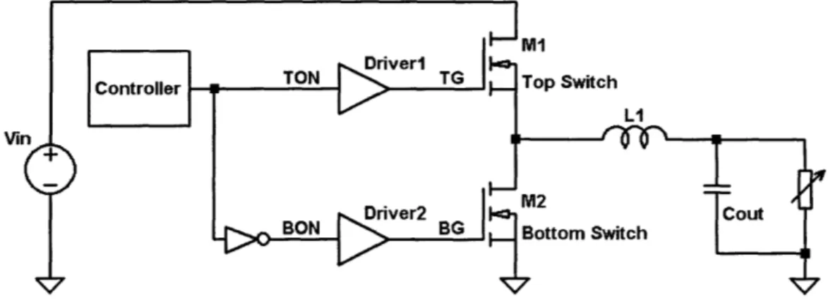
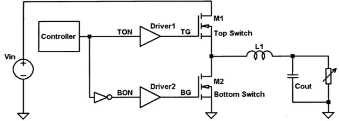
In some applications, SWI is implemented as a MOS switch and SW2 as a Schottky diode (Fig. 2-3). The freewheeling Schottky diode turns on, on its own, shortly after the switch turns off, as the voltage across it rises. On the other hand, a synchronous step-down controller, where both SW1 and SW2 are implemented as MOS switches, as shown in Fig. 2-4, could be more desirable to reduce the conduction loss of Schottky diode and increase efficiency.
M1 Driver1
Controller TON TG Top Switch
VinI
LFor many specific applications, the customers prefer to have a stable switching frequency. Facing voltage variation of input source, this constant frequency controller keeps the same switching period, but adjusts the duty ratio of switches M1 and M2 to regulate the output. This switching frequency is determined by the internal programmable clock, and does not shift significantly with load, line, output, temperature, etc.
In this project, we design a general-purpose constant frequency peak current mode synchronous step-down controller IC, which improves on a previous design -the half version of LTC3855 - and implements an adaptive dead-time control scheme.
2.3
Control Scheme
The most important function of a DC-DC converter is to properly regulate the output voltage over a range of input and load conditions. Hence, it is essential to model the control loop dynamics accurately so that its characteristics can be well understood and the control loop can be appropriately compensated to achieve stability and good transient response for all load ranges and any possible load steps.
2.3.1 Voltage Mode Control
In the voltage mode control, the duty cycle is directly determined by the output voltage
feedback, as indicated in Fig.2-5.
Two major energy storage elements, output capacitor and power inductor, usually give a voltage mode converter a conjugate pair of high-frequency poles, making it hard to com-pensate to achieve loop stability.
2.3.2 Current Mode Control
In peak current mode control, the duty ratio is directly determined by the peak inductor current, and the peak inductor current is set by the output of error amplifier. In implemen-tation, at the start of each clock cycle, the M1 Switch is turned on and the inductor current rises; once the inductor current reaches a threshold value [11], the M1 switch is turned off
Figure 2-5: Feedback signals: when a current mode control scheme is used, the current feedback is required
and M2 is turned on. By regulating the inductor current, the inductor sees no AC compo-nents and is effectively removed from loop dynamics for all frequencies below the switching frequency. Instead of a pair of complex conjugate poles, the current mode regulator has two real-axis poles that make the loop compensation a much easier task. In fact, for all frequencies way below the switching frequency, we only see an abstract transconductance,
Gm2 in Fig.2-6, which is the conversion ratio from the error amplifier output voltage to the inductor current.
VREF _r VU
Gm
1 -Ro
Gm
2RLOAD
[1SCOUT)I
Figure 2-6: Simplified block diagram of an uncompensated current-mode switching regulator
2.3.3
Compensation
As shown in Fig.2-6, the DC gain is determined mainly by the transconductance of error amplifier (EA), denoted as Gm1, and the output resistance of EA, denoted as Ro. The only
relevant low-frequency pole is determined by the output capacitor COUT and load resistor
RLOAD [16] 191.
For example, if this regulator is configured to switched at 500kHz for DDR application from 2.4V input to provide 20A at 1.2V output, the load resistance is RLOAD=6OmQ. If we use an output capacitor of COUT=1500tF, this low-frequency pole is at
1
P2 = 2
1r
R 1.8kHz. LOADCOUTUnless the slope compensation is unreasonably large, the high-frequency pole stays way higher than the switch frequency and we do not need to consider it. Hence, without com-pensation, the loop dynamics will have a crossover frequency close to or higher than the switching frequency.
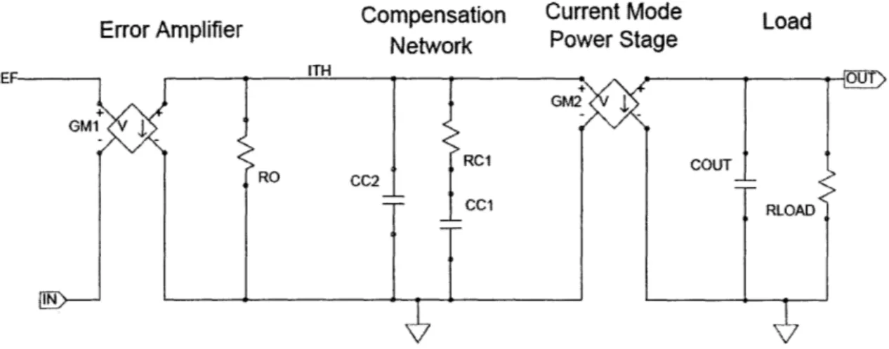
Error Amplifier
Compensation
Network
Current Mode
Power Stage
Figure 2-7: Block-level schematics of an open-loop current-mode regulator
VREF VOUT
- Gm - R0//[1/(sCc2)]//[1/(sCci)+Rc1] Gm2 RLOAD//[1/S COUT)
Figure 2-8: Simplified block diagram of an compensated current-mode regulator
We compensate the current-mode switching regulator by placing an passive compensa-tion network at the error amplifier output, as shown in Fig.2-7. The modified block diagram
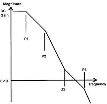
for this compensated regulator is shown in Fig.2-8, compared to the uncompensated version in Fig.2-6. In Fig.2-9, an asymptotical bode plot for the compensated regulator is shown. Adding a dominant pole Pi lowers the crossover frequency. Then with two poles P1 and P2 both before crossover, a zero Z1 is added as well to increase the phase margin. Physically this compensation is easily achieved using a compensation capacitor Cci and a resistor Rci in series on the error amplifier output ITH, illustrated in Fig.2-7. It is also recommended to add a shunt capacitor CC2 to filter as much high-frequency contents. However, the shunt capacitor should be at least ten times larger than the compensation capacitor so that its associated pole P3 is far above the crossover frequency to have minimal effects on loop dynamics. Magnitude DC -Gain
I
0 dBFigure 2-9: Asymptotic bode plot of loop dynamics.
The loop response is given as,
LG(s)
GmiRo(1 + sCcR) Gm2RLOAD1I + s( RoCC1 + RoCC2 + RCc1 ) + S2 Ro Rc1Cc1C2 (1 + s RLO ADCOUT)
S 1+ sCc1R1 1
Gm1RoGm2RLOAD (1 + sRoCc1)(1 +
sRc1Cc2) 1
+
sRLOADCOUTWith the above approximation which is valid if Cci
<
C02 and Roi<
Ro, it is easy to see where the additional poles and zero are:1 P1 = 27rRoCC1' 1 Z1 = I 27rCc1Rc1' 1 21rRc1Cc2
For a numerical example on the compensation of the proposed converter, we could simulate the frequency response on the regulator descripted in Fig.2-7. For this regulator that has an error amplifier with Gm1=2mQ and Ro=2MQ and a regulated current mode power stage of 43S and a load of RLOAD= 6OmQ with CouT=1500pF, without compensation, the crossover frequency is 1.26MHz with -8.6' phase margin, higher than the switching frequency and unstable. With the compensation network at ITH to add a dominant pole, a zero, and a filter pole, respectively at
1 _ P1 Pi=27rRoCC1 - 40Hz ,0H 1 _ Zi 2irRcCc, 13.6kHz, 1 _ P3 = 27rRciCcI 200kHz 2
the crossover frequency is lowered to 47.8KHz (more than one order of magnitude below the nominal switching frequency 500kHz) with 62.80 phase margin, as shown in Fig.2-10.
This stability does not vary much with load. Assuming the load current is smaller and load resistance is larger, the DC gain is larger but the original low-frequency pole is cor-respondingly larger. With the compensation network unchanged, the cross-over frequency and phase margin does not change.
It must be mentioned that the described model above is a very simple model. It only describes the system well for frequencies well below the switching frequency. It also does not model sub-harmonic oscillations. For simplicity, it has completely ignored the effect of slope compensation [16].
V(out)IV(in) 80d-1500 fOd d . 120 ""d-- - ' ,-1-, - - -- r -1-T "k l ,-- - - -r 1 TI- -- -r Ty - -- - -- -rrrn - T- ,1 --- I 90 2 0d B - --. --- -60 -300
I~~ ,to o .. I I ,,, e , , 1gga
40d . ... , ,0 . ,
1Hz~Vou)V~n 10z 10H K0000z10~z 1
-20dB -- + - - -- ---- + + T:--+ + : 7-I --- - -- + - - 7 - -
-.
.20-Figre410 S. s e Bf the u ( adcmest
(otm systems Bd - -- -- --- -irj - - - r-I-T r- -r T r1 -1-1 -- -r -rTTTr ---- ---- - -- - -- -- r i -- -r -g30' 620dB --- - -FIT1-i - A-- + -- + :- - - -- - - +- ---4 0 d Bg 1 1 st ll $868 I ... .I l 8 $0801 8 190" 20dB- --- -0~ -- -~ -0~ z --- - -M - - -- - -- K~ - z---
-Figue 210:Spie smultedBod plts f th unompnsaed top an copen60e ( o m sy ste
d
m s "- "-',si-..
-r 1 T"'h'-r""I.,Ii , , ,,s ,
- - - 1 1A
- --- -' f""T
r1
-O
- - --- -r
Chapter 3
Dead Time Control
3.1
Dead-Time Control
The power switches of a synchronous converter, M1 and M2 in Fig.3-1, are repeatedly switched on and off complementarily by a control signal from the controller. As mentioned in Chapter 1, dead-times are the short period of time when both gate drive signals are off. During this period of transition, device output capacitances charge and discharge until either the other switch turns on or the body diode on one of the switches turns on. When the body diode conducts, it stores charge during the dead time, requiring a reverse recovery period.
Because of the load variation and the internal timing delay due to process variation, non-zero dead-time is generally used. If the dead-time is too short or ever goes negative, huge amount of current could flow through the two switches from the input voltage source to ground. This phenomenon is called "shoot-through". On the other hand, if the dead-time is too long, conduction loss on body diode is large. There should be an optimal dead-time. This optimal dead-time varies with load current and external components. Different external switches have different gating delays and output capacitances, and require different dead time to achieve the highest efficiency.
In most previous commercial controllers, the dead time is fixed internally. We implement a smart dead-time control scheme by sensing the switching node SW and giving precisely controlled timing for the power switches. Then our controller is adaptive to achieve higher efficiency.
3.2
Estimation of Efficiency Improvement
With simple calculation on the body diode power dissipation, we could estimate the possible efficiency improvement with adaptive dead time control. For an application in which the buck regulator outputs a load current of ILOAD at a regulator output voltage of VOUT, if the dead time control scheme successfully reduces the body diode conduction time by AT
for each edge, the energy saving in each clock period is (VD - ILOADRDS(ON))ILOADAT
per edge, where VD is the forward voltage of the switch's body diode and RDS(ON) is the on-resistance of the switch. Assuming the efficiency is close to 1, the efficiency improvement is approximately,
2(VD - ILOADRDS(ON))ILOAD AT 2(VD - ILOADRDS(ON)) AT
A(ef f I T (3.1)
ILOADVOUT VOUT T
A few simple examples will give us a better intuition of how large this efficiency
im-provement is.
1. For a regulator to output 5A at 0.6V switched at 700kHz with 5mQ switches and
improvement of 2*(0.7V - 5A *5mQ *20ns) /(0.6V *(1/700kHz) ) =3.15%
2. For a regulator to output 20A at 1.25V switched at 500kHz, reducing dead time by 15ns would result in an efficiency improvement of 2*(0.7V - 20A *5mQ *15ns)
/(1.25V
* (1/500kHz)) =0.72%
3. For a regulator to output 10A at 1.8V switched at 500kHz, reducing dead time by
15ns would result in an efficiency improvement of 2*(0.7V - 20A *5mQ *15ns ) /(1.8V
* (1/500kHz)) =0.50%
This efficiency improvement becomes more significant as the output voltage goes lower and switching frequency goes higher.
With the continuous demand for smaller external components, the controller needs to switch at higher and higher frequency. Because the digital power consumption is a quadratic function of supply voltage, the power supply voltage of microprocessor and memory goes lower and lower to save power. These two trends of converter technology, higher switching frequency and lower output voltage, make an even more promising perspective of efficiency improvement by adaptive dead time control.
3.3
Prior Art and Other Control Schemes
To achieve best efficiency and avoid shoot-through, the controller needs to adjust the dead-times to the optimum. The optimum dead-time varies with the process variation in con-troller integrated circuit, load, duty cycle, switch characteristics, and etc. If the dead-time is too long, there will be additional conduction loss due to conduction and reverse recovery of the body diodes of the switches. If the dead-time is too short, there will possibly result in simultaneous conduction of both switches, causing efficiency loss and possibly device failure. In most commercially-available DC-DC converter, fixed delays are used to avoid shoot-through, as shown in Fig.3-2. Under this scheme, the bottom gate will turn on only after the top gate turns off, and vice versa. This is a very safe option. However, because of the logic and driver delays, this never creates the optimal solution, in the presence of operating point changes and process variations. This simplest approach leads to low efficiency.
-i - C Load
BON GB
-, Fixed Delay
Figure 3-2: Fixed delays used to prevent shoot-through
Another method of dead-time control to ensure no shoot-through involves the sensing of the SW node. For the TG low and BG high edge, Texas Instrument's TPS2833 achieves no shoot-through by sensing the SW node [12]. If SW is down, that means the top switch is fully off. When SW is down, the bottom driver then starts to charge up to turn on the bottom switch. Because of the delay of bottom driver, the actual dead-time could be much longer than is optimal.
Alternatively, some controllers allow dead-time to be programmed externally as in
LTC3770 [7]. This is a good option for the user, once a specific application is well
charac-terized, at the cost of an additional pin.
Programmable dead-time is particularly convenient for controllers with a digital pulse-width modulator (PWM). In fact, externally-programmed dead-time control, with resolu-tion down to 1.25 ns, has been reported in digitally-controlled switching DC-DC converters [22], [9]. If a DC-DC converter is digitally controlled entirely and now it allows programma-bility of dead-time, it is easy to go a step further and implement various efficient algorithms to optimize the dead-time. People have been using the Maximum Efficiency Point Tracking (MEPT) or similar schemes to select the optimal dead-time [2], [1], [17], [18] in digitally-controlled switching regulators. However, this MEPT scheme requires sensing and com-putation of the input and output powers, which requires significant amount of additional digital logic. It has been pointed out that for a given set of load and output regulation
voltage conditions, the optimum dead-times that lead to highest efficiency result in the minimum switching duty cycle command D [21]. Hence, instead of online maximization of efficiency, online minimization of duty-cycle command could be used instead. Because duty cycle command D is already available in the digital controller, no additional sensing is required. This approach requires relatively small additional digital logic resources and requires no modifications of any gate-drive circuitry [21].
Despite significant effort, fully digital control remains infeasible for our mainstream analog controller IC built on older technologies with minimum gate-length being 0.6 um or larger. In this design, we keep the analog current-mode control.
There have been attempts to use a delay lock loop to align the two gate drive signals in the analog controller, TG and BG, to ensure one switch turns on exactly when the other switch turns off. One complication with this prior design is the turn-off delay time of
MOSFET switch. When external TG falls below the threshold voltage, the switch might
not be off yet. The internal gate voltage may still be above threshold (with the difference owing to distributed gate resistance). Moreover, it takes a few hundred picoseconds to a few nanoseconds to dispel the channel charges. The gate drive signals are not the true signatures of switch-on and switch-off.
On the other hand, the SW node signal gives the true signature of body-diode conduction which directly determines efficiency loss. The longer the body diode turns on, the large the
efficiency loss is incurred. By the looking at SW, we know exactly when the body-diode of the switch starts to conduct. A delay-locked loop can be used to align two edges of switch-on and switch-off signatures. Charge pump has been a popular method for this delay lock loop [3], [15], [20] , but it requires an additional analog servo loop to maintain. Under unforseen conditions, the loop might go unstable and result in shoot-through or worse, losing regulation. For dead-time control where resolution finer than a nanosecond is not meaningful, digital discretization can be used. Hence, in this design, we use a digital delay-locked loop to achieve precise gate-drive timing, and dead-time resolution is defined
by the delay cells used.
tech-nologies with minimum gate-length being 0.6 um or larger, we stay away from full digital control and keep the analog current-mode control. Therefore, it makes sense for us to use the delay-locked loop approach [3], [15], [20] instead of online minimization of duty cycle [21]. However, as done in the digitally-controlled converter with dead-time programmability [22],
[9], we use digital counter instead of charge pump as the memory element in the delay-locked loop.
3.4
Control Scheme with Digital Delay-Locked Loop
To achieve the optimum dead-time, the controller has to be able to adjust the dead-time dynamically. The controller has to extract the dead-time information from electrical signals. The best electrical signals to sense are the top MOSFET gate drive signal, TG, the bottom
MOSFET gate drive signal, BG, and the switch node, SW. These three signals encompass all
the information about the external MOSFET gate voltages, threshold voltages, controller driver strengths, etc. The SW tells the "effective" dead time. If SW is ever one diode voltage above input voltage or one diode voltage below ground, it means the body diode of one of the power switches has turned on; hence, an undesirable conduction loss results.
By sensing these three signals, the controller could extract the dead-times, and adjust them
accordingly using digital logic circuitry.
Unlike the scheme in Fig.3-2, we use variable delays. For the TG low and BG high edge, the overall system is shown in Fig. 3-3.
To controlling Delay2 in Fig. 3-3, we use a digital delay-lock loop which closely resembles an analog phase-lock loop. As shown in Fig. 3-4, SW and BG are sensed through two comparators to produce two edges SBSW and SB]BG. These two edges race each other to make the counter count up or down on the next clock edge. The state of counter determines the variable delay. In the steady state, SBSW and SBBG are very close to each other in each clock cycle, and they alternate to be first.
The algorithm to optimize dead-time on the TG low and BG high edge, is the following,
cG-
c Load
Figure 3-3: TG-off to BG-on edge
SBBG
UP
SB_SW - Latch Counter C[3:01 Delays are on positive edges only
RESET
-Bottom Gate Driver Controlled Delay
TOP > ,> .. , ,,- - BG BG Comparator SBBG
Fixed Delay Top Gate Driver ViN
-TG SW SW Comparat SB_SW
Figure 3-4: The delay-lock loop to align SB..SW and SB_BG signals (parts of this circuitry are shown later in Chapter 4 in more details)
if the SW voltage is higher than input voltage by a fixed threshold voltage or blow the ground by a fixed threshold voltage. The second comparator outputs high if the BG is higher than a MOSFET threshold voltage above ground.
2. Two outputs of comparators are racing each other to be latched and then to set the 4-bit counter. The counter memorizes the state of the last switching cycle. If the BG comparator output is ahead of the SW comparator output, it means that the dead-time is too little; the counter will count up by one LSB on the next cycle. If the SW comparator output comes first, it means that the dead-time is too much; the counter will counter down by one LSB on the next cycle.
3. In steady state, the circuitry will always find one optimal point in the counter and
count up and down alternatively around it.
For the BG low and TG high edge, the overall system is shown in Fig. 3-5. A similar circuit can be constructed, using sensed SW and TG signals as shown in Fig. 3-6. The algorithm to control Delay3 in Fig. 3-5 is the following,
1. SW and TG are sensed through two comparators. The first comparator outputs high
if the SW voltage is higher than the input voltage by a fixed threshold voltage or blow the ground by a fixed threshold voltage. The second comparator outputs high if the TG is higher than a MOSFET threshold voltage above SW.
2. Two outputs of comparators are racing each other to be latched and then to set the 4-bit counter. The counter memorizes the state of the last switching cycle. If the
TG comparator output is ahead of the SW comparator output, it means that the
dead-time is too little; the counter will count up by one LSB on the next cycle. If the SW comparator output comes first, it means that the dead-time is too much; the counter will counter down by one LSB on the next cycle.
3. In steady state, the circuitry will always find one optimal point in the counter and
Delay4C
Load
(-TG
B
-0D3:0] Delay4
Figure 3-5: BG-off to TG-on edge
SBTG UP
SBSW Latch Counter D[30] Delays are on positive edges only
RESET
Top Gate Driver Controlled Delay
TOP ~--- TG-- TG Comparator -SB_TG
SW
Fixed Delay Bottom Gate Driver VIN
- BG SW- SW Comparator - SBSW
Figure 3-6: The delay-lock loop to align SB.SW and SBTG signals (parts of this circuitry are shown later in Chapter 4 in more details)
The overall system, considered both edges, is shown in Fig. 3-7. Additional logic is included to minimize interference and have separate controls on Delay2 and Delay3.
Load
Chapter 4
Chip Design
4.1
Overview
This thesis describes a complete integrated circuit design in a 0.6um BiCMOS process. Accurate evaluation of the efficiency improvement by adaptive dead-time control is only possible through a design fabricated in silicon and eventually measured on well-designed printed circuit board.
This chapter described requirements and trade-offs of each sub-circuit. The LTC3855 was used as a basis for the chip design in this thesis. A block diagram of the designed 24-pin chip is shown in Fig.4-1. For a complete description of pin functions, please refer to Appendix A.
4.2
Internal Supply, Biasing, and Clock
The bandgap reference generates the 1.22V bandgap voltage, and provides a 0.6V reference with resistor dividers for the trimmed buffer to give a precise reference of 0.6V±0.75% at
VREFOUT pin.
An low dropout (LDO) linear regulator with PMOS as pass device is integrated to provide the internal 5V supply with 100mA current capability. With a PMOS transistor as a pass device, the linear regulator is easier to drive than an NMOS LDO, and to achieve
Figure 4-1: Simplified Block Diagram
lower dropout than an NPN LDO. This PMOS LDO is externally compensated by placing a minimum 4.7uF low-ESR tantalum or ceramic capacitor at the INTVCC pin.
This IC also integrates an internal oscillator to provide a clock with frequency config-urable from 250kHz to 770kHz. To set an precise frequency using an external precision resistor, a few devices on the chip need to be trimmed sequentially. The clock oscillation time constant is generated by current charging a capacitor.
T = (4.1)
The charging current is generated by the bandgap voltage and a series of thin film resistors, first scaled with current mirror, and then proportioned by the voltage on FREQ pin. First, the thin-film resistors have to be trimmed for the absolute values of this charging current and the biasing current on FREQ pin to be accurate. Then, the specific current mirror must be trimmed to accommodate the process variations on the absolute value of capacitor.
4.3
Configuration Selection
This circuit block selects between the general-purpose converter configuration and the DDR configuration. In the DDR configuration, the regulated output voltage is shorted to VFB and then divided by half internally. In the general-purpose converter configuration, the regulated output voltage will be divided by an external resistor divider before being applied to VFB pin. In the latter case, the external resistor divider should not be loaded by the internal resistor divider. The easiest way to achieve no loading is using transmission gate, as shown in Fig. 4-2.
The current leakage into the positive input of error amplifier (EA) is on the order of 100nA. For the dividing ratio to be accurate in the DDR configuration, the current running in the divider must be two orders of magnitude higher than 100nA. To have that much current, each resistor must be small. In the general purpose configuration where MN01 is turned off, the 100nA leakage current flows through R01, creating a voltage drop. To reduce this drop, again, the value of R01 must be small. However, such a small resistor would lead
VREFIN
_j
w
Figure 4-2: If CSELB is high, VREFIN is divided by half before applied to the positive input of error amplifier
to higher quiescent power consumption. Additionally, for this simple design, the size of
MN01 must be huge so that its on-resistance will be two order of magnitudes smaller than
the already small resistance values of R01 and R02.
A better but slightly more complicated design could be done as in Fig. 4-3. If the
configuration selection pin CSEL is shorted to ground, transistors MN1 and MP1 are turned on while MN2 and MP2 are turned off; the voltage applied on the VREFIN pin is divided
by half internally before being applied to the positive input of EA. On the other hand, if
CSEL pin is shorted to the internal LDO 5V output INTVCC, transistors MN1 and MP1
are turned off while MN2 and MP2 are turned on; VREFIN is then shorted to the positive input of EA.
For the layout of this block, there are two issues to consider. The MOS transmission gate switch comprises MN2 and MP2, which are directly connected to the package pin, and have risks of being damaged by electrostatic discharge (ESD). Hence, in the physical layout of the circuitry, these devices must have ESD spacing. It means that the drain of these devices are drawn longer, and effectively a resistor is placed in series with the transistor to provide current limit protection. Since the input bias current of the EA is tens of nano amperes, the small amount of resistance created by ESD spacing does not generate much
3SELB PR8F.6 P= 80.6 N-40 CSELB SEB-4B0 EARE~> - VBODY -- CSELBB 20K -R4 -- ELBB
Figure 4-3: If CSEL is grounded, VREFIN is divided by half before applied to the positive input of error amplifier
systematic offset in the regulated output voltage.
The resistor pair R1 and R2 must be precisely matched. In the DDR configuration, the precision of this matching is determines how precise the VTT output is. Any mismatch leads systematic offset of VTT voltage deviated from half of VDD. Fortunately, it is not difficult to achieve ±0.1% matching for integrated thin film resistors on this process platform, if the following rules are strictly observed:
1. Matched resistors have the same width and are sufficiently wide, in this case, 10 times the minimum feature size of the process technology platform;
2. Matched resistors are orientated in the same direction;
3. Matched resistors are on an iso-therm;
4. Resistor segment taps are on an iso-therm to avoid contact therm-couple effect;
6. Matched resistors are placed away from the power devices, specifically, gate drivers
and LDO;
7. Each of the matched resistor pair are an array of resistors in parallel. The array
resistors is interdigitated to have a common centroid.
4.4
Error Amplifier
The basic design of error amplifier is included in Fig. 4-4.
Figure 4-4: Error amplifier design
The PNP input stages allow low common-mode inputs. The NPN differential pair gain stage with PTAT current biasing provides constant transconductance over a wide range of temperatures.
To allow soft start, the error amplifier takes an additional positive input, TKSS. This slow rising TKSS voltage is diode AND-ed with VFB. After TKSS rises above VFB, VFB
takes over to become the positive input. At startup, both inputs of the error amplifier,
TKSS and VFB, are almost near zero voltage. To prevent VITH floating all the way to
the clamp limit and resulting in a few very wide pulses when the regulator starts initial switching, we push asymmetrical currents into the level-shift resistors and get the VITH
driven to ground. As the output ramps up, the common mode of the error amplifier rises; we gradually turn off the asymmetrical level-shift currents. To ensure the accuracy of output voltage, we need to turn off the asymmetrical level-shift current completely before the part settles.
It takes some thought to choose where in the circuit to sense the common mode of the
EA. Since the concern is about the biasing current mirror out of saturation, it is natural
to choose the drain of the MOSFET. However, this node will have large disturbance and the comparator will need very large hysteresis impossible to design. An alternative node to sense is TKSS. It is relatively steady and the comparator will only need small amounts of hysteresis.
4.5
Current Comparator
4.5.1
Current Threshold
The output voltage of the error amplifier, VITH, determines the current threshold at when the top switch turns off in each clock period. In the circuit block named ITHD, voltage
VITH is converted into a current by a fixed ratio RITH. This current, VITH/RITH, later gets reduced by 20uA. The resulting current gets scaled by current mirrors, flows through the offset resistor Roffset in the current comparator, and generates the current threshold.
Hence, the current comparator threshold offset (without slope compensation) is deter-mined by VITH with the following formula,
AVsense = (VIT H - 'offset *
C*
Rof fset. (4.2)For the converter to have almost symmetrical capabilities to sink and source current, AVsense should be designed to cover a wide range from a negative minimum to a positive maximum, as VITH ranges from OV to 1.8V. We must note that when VITH is below 200mV, the current sink NMOS in the output stage of EA could be out of saturation during which the EA no longer functions properly. Hence, VITH should never be driven below 200mV in static state operation. The minimum current sense threshold (negative value) should be slightly bigger in absolute value than the maximum current sense threshold.
Assuming that the power stage of converter uses switches with on-resistance of 2mQ to sink and source up to 25 amperes of current (with 40% ripple, peak current is 30A), a rea-sonable current threshold design is maximum of 60mV and minimum of -72mV. From that,
60 40 20 E 0 -20 -40 -60 -80 0 0.5 1 1.5 2 VITH (V)
Figure 4-5: Current sense threshold versus VITH in this design
we choose in this design, Ioffset = 20uA, current mirror ratio ( 25 or 0 or 60 depending
on whether the ILIM pin is connected to SGND, float, or INTVCC, and Roffset = 4kQ.
4.5.2
Wide Input-Range Current Comparator
As the output voltage is specified to be between 0.3V and 13V, the current comparator has to accommodate a wide common mode input range. For the low inputs, a PNP input
- ILIM = INfVCC -IIM = FLOAT - ILIM = SGND
stage is desired; however, for the high inputs, a NPN input stage is more convenient. An additional voltage comparator was included in this current comparator in order to do both. If the common mode of inputs is below 1.4V, the inputs connect to a pair of PNP transistors and get level-shifted up before fed into the NPN input stages; if the common mode is higher than 1.4V, the inputs connect to the NPN input stages directly. Hysteresis of 300mV is added to avoid oscillation.
4.6
Adaptive Dead-Time Controller
To construct a delay-lock loop (DLL) to align two edges, we use a latch to check which edge comes first, a counter to memorize the state, and a variable delay line. At the front end, we also need to sense the signals. There are in total two delay-locked loops, for the TG low and BG high edge, and for the BG low and TG high edge. Though they are connected differently, the designs are almost the same.
4.6.1 Signal Sensing
Ideally we could use two comparators to determine the times when the power MOSFET body diode starts and stops conducting. Then we could use a delay lock loop to adjust the delay from top gate turn-off logic signal to bottom gate turn-on logic signal until when those two times are very close. In the steady state, the time between the body starts and stops conducting is minimal and perhaps zero.
The SW node, with nanohenry stray inductance and a few nanofarad parasitic capaci-tance, gives ringing at a few hundred megahertz. Occasionally, the ringing is too large in amplitude and too fast to handle. Hence, the SW node signal must be latched and the sensing output is only allowed to change once every clock period.
The SW node can be as high as one body diode forward voltage above the input voltage and can be as low as one diode voltage below ground. That means, numerically, that the SW node can be anything between -1V and 40V. To sense the SW node, a drain-extended thick-oxide MOSFET is required to block high voltage. Unfortunately, under this process
platform, this high-voltage MOS device is non-isolated, and its body is common with P-substrate. A series resistor has to be added to limit the body diode conduction of the blocking device when SW node falls below ground. The RC time constant of this current limiting resistor and the parasitic capacitance is too large for this sensing circuitry to be fast.
P=2.8/0.6 N= 1.410.6 OUT1B + OUT2B MP3 15/5 12ib
Figure 4-6: OUT is high if SW rises 200mV above TD, or 200mV below SGND
P=2.810.6 N=1.4/0.6
INV3
Moreover, the speed of the sensing circuitry depends on the overdrive. If the SW falls from a higher voltage to ground, the overdrive is larger and the circuitry will respond much faster.
Because SW could fall below ground or rise above TD, we have to be very careful in the physical layout of the block to avoid latchup.
4.6.2
Latch
As drawn in Fig.4-7, two falling edges, SB1 and SB2, race against each other to set UP and DOWN. Without loss of generality, we look at the set of latches for events on the TG low and BG high edge. For this edge, SB1 is a logic signal that is 0 if BG is above the power
MOSFET threshold, and SB2 is the logical signal that is 0 if SW is more than 200mV above
the input voltage or more than 200mV below ground. If the falling edge of SB1 comes first, the UP will go high; it means the bottom power switch turns on too early, and the counter should count up. If the falling edge of SB2 comes first, the DOWN will go high; it means the body diode of one of the power switches has turned on before the bottom switch could turn on, and in this case, the counter should count down.
One important detail is that in each clock cycle, we need to reset the SB1/SB2 racing after top power switch is on so that the circuitry is ready for the next racing. Using the rising edge of CLK1 is too early to avoid the ringing of the rising SW edge, and using the falling edge of CLK1 is too late for low-duty case. The required reset signal must arrive earlier than the event of top gate turn-off, so the latches are correctly reset before the next edge of SW falling and the edge of BG turning on; on the other hand, this clock signal has be arrive later than the clock signal for the counter, so that the counter has enough time to settle to its next state before its inputs change. It turns out that the current comparator output ITRP is perfect for the reset task. The ITRP signal always arrives before the edge of SW falling and the edge of BG turning on. Whichever of SB1
/SB2
comes first, the latches reset by ITRP will be ready for the racing. Furthermore, the ITRP signal arrives at least tens of nanoseconds later than the CLK1, which gives ample time for the rising SW signal to settle and avoid false tripping.Figure 4-7: Latch determines which of two falling edges, SB1 and SB2, comes first after each rising RESET pulse
V( c3861:toff-edge:down) 2 .1V . 1.5. -- -. ... 1.5V . ... 4...-... --- ... 0.3. ... ...
2.7V-i.8\
......-....
... ... ... 0.0V- --- ----Figure 4-8: Timing of Edges. From top to bottom, the signals are: ITRP, current compara-tor output and the reset signal for latches; DOWN, logic signal for counter down transition;
UP, logic signal for counter up transition; BG, the gate voltage of bottom power switch;
SB.BG, logic signal that is low if the gate voltage of bottom switch is higher than the
MOSFET threshold voltage (1.6V); SW, the SW node voltage; SBSW, logic signal that is
In Fig.4-8, we see an example of the timing of the delay-locked loop, for the TG low and BG high edge. The current comparator trips first, and the latches get reset. Both UP and DOWN go low after the ITRP signal goes high. Then the SW falls, and the body diode of the bottom power switch conducts. The SW signal goes below ground. The bottom gate turns on, and the BG goes high. In Fig.4-8, the BG go above the MOSFET threshold voltage before the SW falls below ground; hence, the counter counts up so that the variable delay in the bottom gate driver will increase slightly in the next clock cycle.
The timing of these signals on the second delay-locked loop, for the BG low and TG high edge, is similar. An example of the timing is described here. First, the positive edge of internal clock signal comes, and the latches get reset. Both UP and DOWN go low after the CLK signal goes high. Then the SW rises, and the body diode of the top power switch conducts. The SW signal goes above input voltage. The top gate turns on, and the TG goes high. If the TG goes one MOSFET threshold voltage above SW before the SW rises above input voltage, the counter counts up so that the variable delay in the top gate driver will increase slightly in the next clock cycle.
4.6.3
Up-Down Counter
The counter is constructed with 4 toggle flip-flops. A typical toggle flip-flop with minimum sizing is shown in Fig.4-9.
The counter design is shown in Fig.4-10. The counter could count up or count down, depending on which of the two inputs, UP/DOWN, is high at the rising edge of clock. If both up and down signals are received at the clocking edge, the counter will act as it has only received the up signal (see gates 147 and 160 in Fig.4-10). To prevent overflow, additional logic makes sure that this counter will stay at 1111 if it is already 1111 and receives an up signal (see
124, 140,
and 161 in Fig.4-10). Similarly, it will stay at 0000 if it is already 0000 and receives a down signal (see 125, 139, and 162 in Fig.4-10).Figure 4-9: If T=O at rising edge of CLK,