Capacitive Sensing with a Fluorescent Lamp
by
John Jacob Cooley
Submitted to the Department of Electrical Engineering and Computer
Science
in partial fulfillment of the requirements for the degree of
Master of Engineering in Electrical Science and Engineering
at the
MASSACHUSETTS INSTITUTE OF TECHNOLOGY
February 2007
©
Massachusetts Institute of Technology 2007. All rights reserved.
A uthor ...
...
epartmen
ctrical Engineering and Computer Science
February 2007
Certified b
...
Steven B. Leeb
Professor
Thesis Supervisor
Certified by ...I-Al-Thaddeus Avestruz
Student
- Thesis Co-signer
Accepted by...
. .. ...Arthur C. Smith
Chairman, Department Committee on Graduate Students
BARKER
MASSACHUSETT
OF TECHNOLOGY
Capacitive Sensing with a Fluorescent Lamp
by
John Jacob Cooley
Submitted to the Department of Electrical Engineering and Computer Science on February 2007, in partial fulfillment of the
requirements for the degree of
Master of Engineering in Electrical Science and Engineering
Abstract
This work presents a modified fluorescent lamp that can be used as a capacitive sensing sys-tem. The lamp sensor measures changes in the electric fields emitted from the fluorescent bulbs in order to deduce the presence and motion of conductive and dielectric objects be-low the lamp. The prototype lamp sensor demonstrated a detection range of 10 feet for the presence and motion of a human below the lamp. Potential applications of the lamp sensor include proximity detection, motion sensing, security monitoring, activity level monitoring for power management and control and metal or dangerous substance detection.
Thesis Supervisor: Steven B. Leeb Title: Professor
Thesis Co-supervisor: Al-Thaddeus Avestruz Title: Graduate Research Assistant
Acknowledgments
We would like to acknowledge the generous support for this research by the United States Department of Justice, the Grainger Foundation, and the Center for Materials Science and Engineering at MIT.
Contents
1 Introduction
1.1 M otivation . . . . 1.2 Relevant Research. . . . . 1.2.1 Capacitive Sensing . . . . 1.2.2 Biometric and Security Surveillance . . . .
1.2.3 Feedback for Building Power Level Management . . . .
2 The Lamp as an ac Source and Capacitive Models
2.1 Measuring Electric Flux . . . .
2.1.1 The Bulb as an Alternating Voltage Source . . . . 2.1.2 The Alternating Current Measurement . . . .
2.1.3 The Capacitive Sensing Abstraction . . . . 2.2 The Practical Alternating Voltage Source . . . .
2.3 Capacitive Sensing Models . . . .
2.3.1 Capacitance Model . . . .
2.3.2 Dielectric Reluctance Model . . . .
3 Signal Conditioning
3.1 Differential Transimpedance Front-End Amplifier for Current-Mode De-tection . . . .
3.1.1 Differential Front-End Operating Principles . . . .
3.1.2 Differential Transimpedance Amplifier Input Characteristics . . . 3.1.3 Feedback ComDensation . . . . 19 19 21 21 23 24 27 27 29 31 34 35 38 38 40 45 46 48 51 57 . . . .
3.1.4 Common-Mode Rejection ... ... 63
3.2 Synchronous Detection Operating Principle and Implementation . . . . 69
3.2.1 Synchronous Detection Operating Principle . . . . 69
3.2.2 Synchronous Detection Implementation . . . 74
3.3 Analog to Digital Interface . . . 80
3.4 Noise Sources . . . 83
4 Expected Output Behavior 93 4.1 Reduced Reluctance and Capacitance Models . . . 93
4.1.1 Stray Capacitances and Negligible Capacitances . . . 94
4.2 Expected Output Response . . . 96
4.2.1 Calculated Output Response . . . 97
4.2.2 Simulated Output Response . . . 102
5 Results, Data Analysis and Demonstration 107 5.1 Measured Output Response and Range Test Data . . . 108
5.2 Signal Source Magnitude Calibration . . . 111
5.3 Real-Time MATLAB Demonstration . . . 113
6 Multiple Electrode Pair System and Further Work 115 6.1 Controlling the Sensing Range . . . 115
6.2 A Prototype Mixed-Signal System for Multiple Electrode Pair Measurements 117 6.2.1 Initial Data and Conclusions . . . 121
6.3 Limitations and Further Work . . . 123
6.3.1 Possible Immediate Improvements . . . 125
A Lamp Sensor Application Notes 127 A. 1 Nulling the Output . . . 127
A.2 Practical Considerations for a Predictable Output . . . 127
B Software 131 B.1 MATLABCode . . . 131
B.1.1 B.1.2 B.1.3 B.1.4 B.1.5 B.1.6 B.1.7 B.1.8 B.1.9 B.1.10 B.1.11 B.1.12 B.1.13 B.1.14 B.1.15 B.1.16 B.2 C Code B.2.1 B.2.2 B.2.3 takedata.m ... postprocess.m . . clearv.m . . . . . PlotADCroll.m . Demo.m . . . . . Compensation2.m Syncdet.m . . . anacap5.m . .. datatest.m . . . . openloopcomp.m idiffthesis.m . . datatest.m . . . . scandata.m . . . clearens.m . . . storecontrol.m storedata.m . . . for the PIC . . . adc.c . . . . Demomaster.c. Demoslave.c C Schematics and PCBs C. 1 PCB: Front-End Only. C.2 PCB: Full Channel . . . 131 . . 132 132 . . 132 . . 134 . . 136 . . 137 . . 138 . . 140 . . 141 . . 142 . . 143 . . 143 . . 144 . . 144 . . 145 . . 145 . . 145 . . 150 . . . 156 161 161 162 . . . . . . . .
List of Figures
1-1 FSK modulation circuit for transmitting data using a standard fluorescent
bulb [15] . . . . 19
1-2 Electric field strength simulations of a human walking below a fluorescent
lam p. . . . 2 1
1-3 Lumped element model of a MEMS accelerometer[24]. . . . 22
1-4 Generalized block diagram depicting the common detection scheme in the research presented on capacitive sensing . . . 22
1-5 An electric field depiction of a capacitive sensing scheme for fingerprint
reading[29]. . . . 24
2-1 Lumped capacitances couple the bulb surface to the electrode and to the
ground reference. A voltage relative to the ground reference can be
mea-sured at the electrode as (imeas X Zmeas). . . . .. . . . . 28
2-2 A conducting target introduces a change in the capacitive coupling and the change in the electrode voltage relative to the ground reference can be measured. A voltage relative to the ground reference can be measured at
the electrode as (imeas x Zmeas) . . . . .. . . . . .. . . . . .. . . .. . 29
2-3 The measured fluorescent bulb voltage (a) and current (b) to determine the nominal lengthwise resistance. . . . . 30
2-4 The high-impedance ballast current source drives the low-impedance bulb. 31
2-5 The Thevenin equivalent circuit shows a low-impedance voltage source. . 31 2-6 A two-electrode set up for differential measurements . . . . 36 2-7 A typical lengthwise voltage profile of a fluorescent bulb[10]. . . . . 36
2-8 Two effective lumped and symmetric alternating voltage sources from the
segments of the bulbs nearest the electrodes with the ballast connections to
one of the bulbs reversed. . . . . 37
2-9 A lumped element capacitive model of the lamp sensor and target system. 39
2-10 A lumped element dielectric reluctance model of the lamp sensor and target
system . . . . 43
3-1 Schematic of the Low-Noise Analog Front-End Amplifier. . . . 48
3-2 The concept of separating differential-mode signals from common-mode
signals. . . . 49
3-3 A typical op-amp negative feedback connection . . . 50
3-4 Differential input current in a differential amplifier . . . 51
3-5 A fully differential amplifier taking into account shunt impedances from
the measurement nodes to incremental ground. . . . 52
3-6 The half-circuit with incremental grounds for calculating the effect of the
shunt impedance on the output voltage. . . . 53
3-7 A current divider between the currents in the amp circuit with the
op-am p rem oved. . . . 54
3-8 A differential transimpedance amplifier measuring current through
capaci-tive im pedances . . . . 57
3-9 Closed-loop bode plots of the voltage transfer function of the Front-End
amplifier with a fixed differential input capacitance. Plots are shown with
various feedback capacitances 0 < C < 62 pF and Rf = 1 MQ. . . . 59
3-10 The half-circuit for calculating the stability of the differential front-end
am plifier . . . . 60
3-11 The block diagram for the differential closed-loop front-end amplifier system. 60 3-12 Bode plot of the loop transfer function for the uncompensated system (Cf =
3-13 Bode plot of the compensated loop transfer function showing good phase
margin. The addition of Cf in the feedback network is a form of lead
com pensation. . . . 63
3-14 Bode plot of the compensated system with extra input capacitance showing degraded but acceptable phase margin. . . . 64
3-15 Simplified schematic of THS4140[38]. . . . . 65
3-16 The differential amplifier with component mismatches. . . . 66
3-17 Basic plot of 1/f noise and thermal noise densities . . . 70
3-18 Plots of the voltage noise spectral densities for the THS4140 (a) and AD8620 (b)[38][36]. . . . 70
3-19 Block diagram of the synchronous detection system . . . 71
3-20 Frequency-domain plot of the modulating signal, carrier signal, and ampli-fier noise. . . . 72
3-21 Demodulation of the amplified up-modulated signal by multiplication with the carrier. . . . 73
3-22 Output of the synchronous detection system. . . . 73
3-23 Normalized output response of the synchronous detector plotted against phase error between the measured signal and the clock signal. . . . 74
3-24 Clock generation circuit[39]. . . . 75
3-25 Fully differential square wave multiplier[41]. . . . 76
3-26 Fully differential LPF . . . 77
3-27 The full schematic of the analog receiving network. . . . 79
3-28 Connection diagram of the analog-to-digital interface. . . . 82
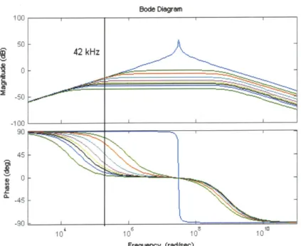
3-29 Voltage spectral density of the differential output of the front-end amplifier from dc to 20 kHz showing the 1/f corner. . . . 85
3-30 Voltage spectral density surrounding the carrier frequency of 42 kHz at the differential output of the front-end amplifier with no input signal and the inputs open-circuited. Interference from other lamps appear as stray signals in the plot. . . . 86
3-31 Differential circuit for calculating differential output voltage noise from
input-referred current and voltage noise sources. . . . 87
4-1 The full capacitive model of the lamp sensor and target system. . . . 94
4-2 Reduced capacitance model. . . . 95
4-3 Reduced dielectric reluctance model. . . . 96
4-4 Incremental capacitive circuit extracted from the physical model and inter-faced with the transimpedance amplifier. . . . 98
4-5 A capacitive half circuit for calculating differential current in the capacitive system . . . . 99
4-6 A dielectric reluctance half circuit for calculating differential electric flux in the capacitive system. . . . 99
4-7 A screenshot of the Fastcap model for the horizontal lamp setup. . . . 103
4-8 A screenshot of the Fastcap model for the hanging lamp setup. . . . 103
4-9 An example of the Fastcap output matrix. . . . 104
4-10 A plot of the simulated output voltage as a human target passes in front of the lam p. . . . 105
4-11 A plot of the simulated output voltage as a human target passes below of the lam p. . . . 105
5-1 A photograph of the cart-mounted prototype lamp sensor. . . . 107
5-2 Examples of plots of sample detections from the range test. [Configuration 44x5] ... ... 109
5-3 Overlayed plots of the real output response for calibration of V . . . 112
5-4 Tabulated data of the peak deviation of the real output response for calibra-tion of V . . . 112
5-5 A screenshot of the real-time Matlab demo. . . . 114
6-1 A plot of the simulated output voltage for varying electrode spacings. . . 116
6-2 A photograph of the multiple electrode system setup. . . . 118
6-4 The connection diagram for the prototype multiple channel system . . . 120
C-I A PCB for the front-end amplifier . . . 161
List of Tables
2.1 Capacitance descriptions and nominal values for the full capacitance model. 40
3.1 Significant Noise Sources . . . . 92
4.1 Conductors in the Fastcap model . . . 104
5.1 Detection Data p-values for Various Electrode Configurations at the Limit
of the Detection Range. . . . .111
6.1 Detection Data p - values for vertical scans of a human walking below the
Chapter 1
Introduction
1.1
Motivation
The ubiquity of fluorescent lighting in public, commercial and work spaces motivates in-vestigation into the potential to exploit the already in place infrastructure of fluorescent lamps for multi-use applications. For example, [15] describes a system which transmits data by modulating the frequency of the light radiated by a fluorescent lamp. With this system, each fluorescent light becomes a versatile data access point that can be used, for example, to transmit location specific audio data to blind customers in a shopping area. The frequency modulating ballast for "Talking Lights" is shown in Figure 1-1.
Figure 1-1: FSK modulation circuit for transmitting data using a standard fluorescent bulb[15].
The infrastructure provides an omnipresent, controllable light source and alternating elec-tric field source. If the electronics for the system that exploits the fluorescent lamp infras-tructure are engineered to not modify the outward appearance and operation of the lamp, a certain level of discreteness is achieved despite the omnipresence of the electronic system. Electronics that are incorporated into the lamp ballast can be installed cost-effectively and without the knowledge of the person who installs them. The electronics do not have to be particularly low-power because they will have access to the same utility power that the lamp ballast uses. Finally, electronics that are installed in all of the fluorescent lamps in a public space result in a macroscopic system that can be networked and controlled remotely. For instance, a power-line modem or a wireless connection could be used to interface a remote PC with each of the lamp sensors.
In particular, the characteristic of the fluorescent lamp infrastructure that this work ex-ploits is that, under normal operation, fluorescent lamps provide an alternating electric field that can be used for sensing applications. This work demonstrates electronics and tech-niques to measure changes in the electric fields under the lamp and to deduce the presence and motion of conducting or dielectric bodies.
Figure 1-2 shows simulations of how the electric field strength under a fluorescent light bulb changes in the space below the lamp as a human walks by. In the simulation, the flu-orescent bulb is a resistive oblong conductor with a piece-wise linear voltage distribution that approximates the low-frequency lengthwise voltage profile of a real fluorescent bulb. The backplane of the lamp is grounded as is the ground below the human. The human is modeled as a six foot tall rectangle composed of salt water. The electric field distribution below the lamp is asymmetric because the voltage profile of the fluorescent bulb is asym-metric. The color gradient from blue to red represents increasing electric field strength.
Potential applications of the sensor system presented in this work include security mo-tion detecmo-tion, activity level monitoring for power level management, biometric surveil-lance, and metal or dangerous substance detection. Examples of spaces in which these applications would be appropriate include airports, commercial buildings, prisons, and gov-ernment or secure buildings.
Figure 1-2: Electric field strength simulations of a human walking below a fluorescent lamp.
1.2 Relevant Research
1.2.1
Capacitive Sensing
This work approaches the lamp sensor system as a capacitive sensor in order to simplify the process of measuring electric field changes below the lamp. Therefore, relevant research includes the entire discipline of capacitive sensing and applications. Many references can be cited on this topic; a few are reviewed here.
One of the most contemporary and common applications of capacitive sensors is in micro-electromechanical systems (MEMS) accelerometers. In this case, the MEMS device acts as a capacitive structure and is interfaced with sensing electronics to measure acceler-ation from the displacement of a mass in a mass-spring system. For example, Hao Luo has presented his research in micro-machined lateral accelerometers [19]. Also, Bliley [2] has presented research in the application of capacitive accelerometers for personal motion data logging. Anwar Sadat has presented research on the design of a MEMS capacitive sensor interfaced with CMOS sensing electronics. Figure 1-3, taken from Sadat[24], shows an example of the capacitive measurement of a displaced proof-mass to deduce acceleration.
In addition to MEMS accelerometers, capacitive sensing is a useful sensing technique in situations requiring non-contact and even high-accuracy measurements. These measure-ments can be used to measure the physical orientation of conducting and dielectric bodies in 2D and 3D spaces. D. Marioll of the University of Brescia, Italy, has published the paper "High-accuracy Measurement Techniques for Capacitance Transducers[201." In Marioll's paper, techniques for signal conditioning and accurately measuring capacitances of interest
Vm+ Q-S CS Movement, x 9 1 sping rRI 1m CuZ Pofmass: Vm VS Vm-Anchor VM+
Vm-Figure 1-3: Lumped element model of a MEMS accelerometer[24].
J. R. Smith of the Media Laboratory at MIT has published "Field mice: Extracting
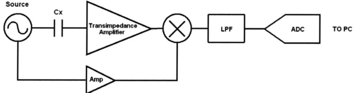
ge-ometry from electric field measurements[25]." In Smith's research the goal is actually to detect the human hand as a conducting object amongst electric field sources and sensors. This research in particular has some similarities to the research in this work. The capac-itive sensing circuit topology and methodology in the work described above consistently demonstrates similarities to the topology in this work. A generalized block diagram of the common topology is shown in Figure 1-4.
Source
CX
Transnpedance LPF ADC TO PC
Figure 1-4: Generalized block diagram depicting the common detection scheme in the research presented on capacitive sensing.
The generalized topology uses an ac signal source to drive current through the
the capacitance, Cx with a transimpedance amplifier (although Sadat's system is an ex-ample in which the sensing electronics take a voltage measurement using an operational transconductance amplifier (OTA)[24]). The common topology then uses some form of synchronous detection to condition the output of the front-end amplifier by multiplying the measured signal with the signal source. Finally, the signal is digitized for processing with a computer. The topology presented in this work, although similar on a high level to many of the topologies presented for capacitive sensing, is designed particularly for the lamp sensor application and presents some particular advantages over the common detection topologies that allow for useable detection ranges in the unfriendly and not well-controlled environ-ment below a fluorescent lamp.
1.2.2
Biometric and Security Surveillance
One of the principle motivating factors of this research has been the potential to use the lamp sensor as a security detection device. This work presents circuitry and detection meth-ods which prove the lamp sensor to be useful at the very least as a motion detection system. Further, we are exploring the possibility of more sophisticated biometric surveillance in which we will attempt to extract vertical profiles of the dielectric and conductive make-up of a person below the lamp by controlling the sensing range. The ability to perform Elec-trical Capacitance Tomography may be possible by controlling the sensing range with the system that will be presented in Chapter 6. Some relevant research in discrete, widespread security surveillance systems as well as electrical capacitance tomography (ECT) is sum-marized here.
Fong [11] has presented research in security systems in which he discusses a widespread networked security surveillance systems using web-based communication to interface mul-tiple security devices. The lamp sensor could be used in this context as a security device which can be interfaced on a large scale with other lamp sensors.
Professor Wuqiang Yang at the University of Manchester Institute of Science and Tech-nology, U.K. has presented research in ECT[34]. Professor Yang's research uses capacitive sensing techniques to map the electric fields in spaces occupied by conductive and
dielec-tric liquids and gases.
Thomas Heseltine has presented research in ECT in which he uses capacitive sensors to generate a 3D map of a human face[14]. Applications of Heseltine's work include security, surveillance, and archive searching. In this case, Heseltine treats the face as an "eigensur-face." This refers to the "inverse problem" that Yang [34] discusses in his research in which the shape of the conductive or dielectric body measured by the capacitive sensor system is deduced from multiple electrode measurements. Marco Tartagni presents a capacitive sensing scheme for non-contact measurements of human fingerprints for identification pur-poses. Figure 1-5 shows the electric field depiction of the capacitive sensing scheme that Tartagni employs in his fingerprint reader.
(a)
(c)
Fig. 4. (a) Parasitic feedback capacitance and (b), (c) sensing principle.
Figure 1-5: An electric field depiction of a capacitive sensing scheme for fingerprint reading[29].
1.2.3 Feedback for Building Power Level Management
Commercial buildings and residences and industrial shops and factories are often designed primarily to fulfill their role of providing occupants with space. The cost of operating these buildings is frequently a secondary consideration, at least until operating expenses force a reconsideration of operating behavior and the installed physical plant. There is
an exploding interest in making buildings more economical to operate while maintaining occupant comfort. Operating costs matter, and will become even more important in the future. A unique opportunity for energy conservation is becoming technically feasible.
We are developing mathematical tools to develop accurate models of a building's en-vironment (temperature, for example) in response to important variables like occupancy, electrical loading, outdoor weather, and heating, ventilation, and air-conditioning (HVAC) operating parameters. These models require fine-grain occupancy measurements taken at known positions in a building. Easy proximity detection of people makes it easy to collect this data. These models make it possible, for example, to examine the effect of a reduction in HVAC plant operating costs on occupant comfort[6].
Professor Steven Leeb has presented research in the area of non-intrusive load moni-toring for building power level management[16] [9] [17]. Leeb's research examines non-intrusive power building-level power network analysis for improved efficiency in power usage.
Chapter 2
The Lamp as an ac Source and
Capacitive Models
The first task in understanding how a fluorescent lamp can be used as a sensing device is in characterizing the lamp as an electric signal source. With sufficient understanding of the signal source, the lamp sensor system can be simplified and an electrical model can be extracted that will predict the output response of the system. If the output response of the real system matches the response that was predicted by the model, then we can be confident that we understand the basic operating principles behind the lamp sensor and thus
make intelligent decisions in engineering the system performance.
2.1 Measuring Electric Flux
Generally speaking, we initially expect the lamp sensor to work as follows. Under normal operation, the bulb surface potential varies with respect to an incremental ground reference as the ballast drives current through it. The incremental ground reference for the lamp sen-sor is discussed in Section 2.2.1 Electric field couples the surface of the bulb to conducting surfaces below the lamp and to the ground reference. The electric field below the lamp can be sensed by measuring the voltage of an electrode placed in front of the bulb relative to
'The effect of earth-grounded surfaces including the backplane behind the bulbs and the floor below the lamp will be examined in Chapter 4.
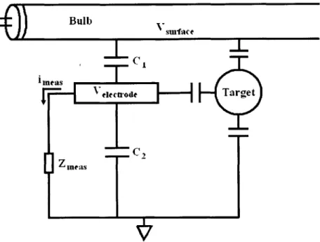
the ground reference. The behavior of the electric fields can be modeled with lumped ca-pacitances between the conducting surfaces. The specifics of the capacitive model used in this work will be developed in the coming Chapters. A qualitative picture of the capacitive coupling between the conducting surfaces and the ground reference is shown in Figure 2-1, in which the voltage of the electrode is the result of the capacitive voltage divider formed
by C1 and C2 and it is measured as the product of the current imeas and the impedance
Zmeas.
)
Bulb CI Vecictrode-ineasF
21
(Figure 2-1: Lumped capacitances couple the bulb surface to the electrode and to the ground reference. A voltage relative to the ground reference can be measured at the electrode as
(meas X Zmeas).
When a conductive or dielectric target such as a human is present below the lamp, it distorts the electric field below the lamp and therefore changes the capacitive coupling between the conducting surfaces. The change in the capacitive coupling can also be mea-sured at the electrode as a change in the electrode voltage relative to the ground reference.
A qualitative picture showing the capacitive coupling below the lamp with a conducting
target is shown in Figure 2-2.
The particular manner in which the electric field distribution changes and therefore how changes in the capacitive coupling are measured, depends on how the source is character-ized. If the source were characterized as an alternating current source or a high impedance
Bulb
smface
7 electrode Target
C,
Figure 2-2: A conducting target introduces a change in the capacitive coupling and the change in the electrode voltage relative to the ground reference can be measured. A voltage relative to the ground reference can be measured at the electrode as (imeas X Zmeas).
source, then the total electric flux from the surface of the bulb would be fixed. In that case, a target would divert some of the electric flux away from the measurement electrode and we would measure a reduction in the electric flux incident on the electrode. If the source were characterized as an alternating voltage source, or a low impedance source, then the surface potential of the bulb would be fixed relative to the ground reference and the total electric flux from the surface of the bulb would vary in response to a target. Therefore, the first task is to understand whether the bulb should be characterized as an alternating current source or an alternating voltage source.
2.1.1
The Bulb as an Alternating Voltage Source
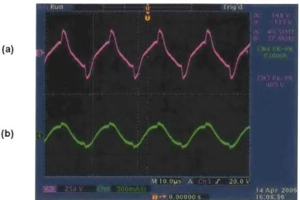
To determine the appropriate source characterization, consider the source and loading impedances. The lengthwise impedance along the length of the bulb was measured as the ratio of the root-mean-square (rms) voltage across the bulb to the rms current through the bulb. This measurement gives a nominal resistance of 900 Q. Scope traces of the bulb current and voltage are shown in Figure 2-3.
(a)
(b)
Figure 2-3: The measured fluorescent bulb voltage (a) and current (b) to determine the nominal lengthwise resistance.
The loading impedances on the source will be capacitive impedances from the surface of the bulb to the conducting bodies in the system. These capacitances will be shown to have maximum nominal values of about 1 pF. The fundamental signal frequency of the
source, w, is taken from the ballast operating frequency of 42 kHz. Therefore the smallest
nominal capacitive impedance in the system will be approximately 1
IZc,min
= 1 (2.1) WCmax 1 - (2.2) 27r x 42 kHz x 1 pF Zc,minl = 3.8 MQ. (2.3)Conducting bodies below the lamp will divert some alternating current via these ca-pacitive impedances providing a high-impedance path from one point on the surface of the bulb to other conducting surfaces or to the ground reference. Although the ballast itself is a high-impedance current source, the capacitive impedances from the bulb surface to the conducting and dielectric bodies below the lamp will see the bulbs as a low-impedance voltage source. Figure 2-4 shows the situation in which the ballast current drives the low-impedance bulb. Alternating current is diverted from the surface of the bulb at points
'ballast
(
S+00 na
Vsurface
Figure 2-4: The high-impedance ballast cur-rent source drives the low-impedance bulb.
Signal Source
800 n
Ri load
IIR
Vsurface \c=3.8
Figure 2-5: The Thevenin equivalent circuit
shows a low-impedance voltage source.
between the two ends of the bulb. Considering only one point at a time, labeled in Figure
2-4 as Vsurface, the bulb and ballast source can be drawn as a Thevenin equivalent circuit
shown in Figure 2-5. In the Thevenin equivalent circuit, the source appears to the capaci-tive load as a low-impedance voltage source. The bulbs as an electrical signal source are
therefore treated as an alternating voltage source.
2.1.2
The Alternating Current Measurement
Considering the bulb surface as an alternating voltage source implies the manner in which the target will distort the electric fields below the lamp and therefore the manner in which the target will be detected. In order to develop intuition about the way that the electric field must change in response to a target, first note that the electric field (E-field) must terminate perpendicularly to any conducting surface (inasmuch as that surface is perfectly conducting). Second, note that the potential difference between any two points is equal to the line integral of the electric field vector between those two points.
(2.4)
The fact that the bulb acts approximately as a voltage source or a low-impedance source means that the potential difference between a fixed potential surface and the bulb must re-main constant despite electric field distortions. Therefore, a conducting target in the
tion field distorts the electric field in such a way that the field lines terminate perpendicular to the target surface and that the line integral of the vector electric field between any two fixed potentials remains constant.
The E-field perpendicular to a conducting surface is proportional to the surface charge density on that surface. In other words, the total electric flux on a conducting surface is
equal to the ratio of the total surface charge
Q,
to the dielectric constant E of the mediumin which the E-field exists:
(De
=LA~
E
dA-SE,
(2.5)
where 4e is the electric flux calculated as the surface integral of the electric field. If
Q,
onthe surface of the conductor is reduced, the total E-field incident on the conducting surface or (De is reduced and vice versa. The presence of the conducting target in the detection field means that some charge on the surface of the target can balance some of the charge on the surface of the bulb or any other conductor in the system by the electric flux linking the two
surfaces. Therefore, we intend to measure electric flux DE, at the electrode by measuring
varying surface charge on the electrode in order to measure electric field distortions below the lamp.
The ballast drives the fluorescent bulb with an alternating current. Assuming that the bulb has some finite impedance, there is some alternating voltage drop across it. Taking only the segment of the bulb behind the electrode, the potential there varies as an ac voltage about some average potential with the ballast operating frequency. The time-varying bulb surface potential 0(t) is
(t) = E (r, t) - dr-, (2.6)
where R is the radius of the bulb. The time-varying E-field, A E(t), from each incremental bulb surface area segment, AA, varies with the distance from the bulb surface as
AQ(t)
AE(t) = 4r 2 (2.7)
direction radially outward from the center of the bulb. Then, from (2.6),
(t) = AQ(t) (2.8)
47rER
Therefore, the surface charge on the bulb varies as the surface potential varies with the ballast operating frequency. Finally, the electric flux from the surface of the bulb alternates with the operating frequency of the ballast from (2.5) and (2.8) and that alternating elec-tric flux couples the bulb surface to other conducting surfaces including the electrodes. In order to measure the electric flux at the electrode, a measurement is taken of the alternat-ing current that couples from the surface of the bulb to the electrode. The time-varyalternat-ing incremental surface charge on the electrode is
LAQ(t) = CVDIe(t), (2.9)
where A4De(t) is the incremental electric flux at the electrode and the incremental surface potential in terms of the incremental electric flux from the surface of the bulb is
/~e(t)
AO(t) = .eR (2.10)
47rR The current measured at the electrode is
d
i(t) = -Q(0) (2.11)
dt
where
Q(t)
is the integral of the incremental surface charge on the electrode over thesur-face area of the electrode. From (2.11) and (2.9), each frequency component of the alter-nating electric flux at the electrode gives rise to a frequency component of the alteralter-nating current at the electrode. For each frequency component of the alternating electric flux,
4e (t) = 4>eo sin(wt). (2.12)
of electric flux as
i(t) = e T4e(t). (2.13)
Finally, the alternating current in terms of the magnitude of the electric flux at the electrode is
i(t) = Ew4I cos(Wt). (2.14)
There is a phase shift of 90' between the alternating electric flux and the alternating current measured at the electrode. The alternating current measured at the electrode then is a 90' phase shifted version of the alternating electric flux scaled by the factor 6w. Then, the conducting electrode can be thought of as an alternating electric flux-to-alternating current
transducer that adds an inherent 900 phase shift and scales by the factor EW for correct
units. In order to measure electric flux with a current measurement, the frequency of the
alternating surface potential on the bulb must be nonzero due to the factor of W in i(t), so
our source must be an ac electric signal source.
2.1.3
The Capacitive Sensing Abstraction
Capacitance between two conductors is the ratio of the total charge on each conductor to the voltage between the two conductors for all time:
Cvc(t) = Qc(t). (2.15)
In (2.15), C is constant in time, vc(t) is the alternating voltage between the two conductors and Qc(t) is the alternating total surface charge on either conductor. Then, capacitance can
be rewritten in terms of alternating electric flux, 4Ie(t), as
E L fE(t) .dA _D e(t)
C = = (2.16)
fE (t ) - i vc M Solving for the alternating current at the electrode,
i(t) = --
Q
M,(2.17)
with the definition of capacitance,
i(t) = +(Cvc M) = d (EDe(t)Vc(t)) (2.18)
d d
= g e(e (t) = E d[eoSin(Wt). (2.19)
-dt dt
Therefore, the current in a capacitor in terms of the magnitude of the flux linking its two conductors is
i(t) = eweo cos(Wt) (2.20)
which is consistent with the form of i(t) in (2.14). So we have a capacitive sensor for which
vC(Wt) -D ~e (t) _ eIeo sin(wt) (2.21)
oc~t) C C (.1
from (2.16). Then, from (2.14) and (2.21) the capacitive reactances are as expected:
______)_ 64 eo 1
XC(w) = C(wt)= = oe - - (2.22)
lic(wt)l CEW(Deo WC'
so that for a fixed magnitude of alternating voltage vC (t) , the alternating current magnitude
ic(t)
I
increases with capacitance C and frequency w. It is more convenient to measure the rms current at the electrodes,irms = ji(t)= - cw4I, (2.23)
in terms of, Ie, the magnitude of each sinusoidal frequency component of the electric flux.
For an arbitrary periodic drive the currents will add in quadrature according to the electric flux magnitude i, of each frequency component n with frequency wn as
irms = - (2.24)
2.2
The Practical Alternating Voltage Source
In the lamp sensor system, detection is approached with a differential and nulled measure-ment between two electrodes. The differentially nulled measuremeasure-ment requires symmetry
about the center of the lamp. Therefore, the two electrodes need to couple to two equiva-lent voltage sources. The necessary symmetry is achieved using two electrodes spanning two bulbs symmetrically as shown in Figure 2-6.
Electrodel Electrode2
Bulbi
Bulb2
Figure 2-6: A two-electrode set up for differential measurements
The lamp segments behind each electrode can be abstracted as effective alternating voltage sources. Ideally, this configuration provides two lumped and symmetric effective voltage sources behind the electrodes. Under normal operation, the ballast drives the flu-orescent bulbs in phase, meaning that the current through each bulb is instantaneously flowing in the same direction. The profile of the lengthwise bulb voltage due to the bal-last current relative to one end of the bulb is nonlinear and asymmetric. A typical voltage profile of a fluorescent bulb is shown in Figure 2-7 provided by [10].
Volag
distance fra cathode
Figure 2-7: A typical lengthwise voltage profile of a fluorescent bulb[10].
ballast connection to one of the two bulbs is reversed so that the bulbs are driven opposite each other. In that case, with the electrodes equidistant from the center of the lamp, the summed voltages relative to the center of the lamp due to the bulb segments behind the electrodes are the same for the both electrodes.
Ballast 1
L ._
0E"_
ns2 Bulb I Bulb 2 I- V a - aEffective Source I Incremental source GND Effective Source 2
Figure 2-8: Two effective lumped and symmetric alternating voltage sources from the seg-ments of the bulbs nearest the electrodes with the ballast connections to one of the bulbs reversed.
With two symmetric alternating voltage sources, the lamp as an alternating voltage source can be lumped and abstracted as in Figure 2-8. The two effective voltage sources
V,1 and V2 are equal to each other with respect to the center of the lamp. Therefore, the
ground reference for the differential measurement is the potential at the center of the lamp and it is labeled in the picture as "Incremental source GND". In the capacitive measurement scheme, the effective magnitude of the voltage sources is some ac rms voltage. Obtaining a value for the effective magnitude, however, is complicated because it depends on the particular geometry of the lamp, the electrode configuration and on the nonlinear voltage profile of the bulbs. Because the value of the voltage source magnitude is only useful for simulating absolute responses, it is not directly measured, although it will be inferred in Chapter 5 by comparing a real response to a simulated response.
2.3 Capacitive Sensing Models
With an understanding of the lamp as an electrical signal source, a capacitive model can be constructed that will be used to model the behavior of the electric fields below the lamp in response to a conducting or dielectric target. The abstraction of the effective and symmetrical voltage sources allows for a simplified lumped element model of the lamp sensor and target system. That lumped element model will be presented in two ways in this section.
2.3.1
Capacitance Model
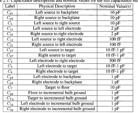
As shown in section 2.1.3, measuring the electric flux that is incident on the measure-ment electrodes amounts to measuring capacitances in the lamp sensor and target system. Therefore, it is simplifying and useful to build a lumped element model of the capacitances between each of the conducting bodies in the lamp sensor and target system. Using this model, intelligent decisions about detection schemes can be made and an understanding of the output response of the lamp sensor system to a specific motion or body below the lamp can be achieved. Interfacing the capacitive model with the signal conditioning electronics of Chapter 3, and simulating the capacitances in the system, an expected output response can be attained.
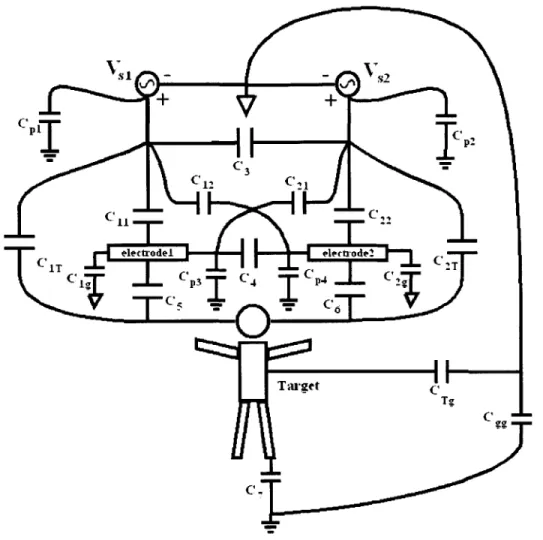
By taking into account the capacitances between each of the conducting or dielectric
bodies in the lamp sensor and target system, a full capacitive model like that in Figure 2-9,
is obtained. In this model, the sources are shown as voltage sources Vj1 and V12, referenced
to the ground reference at the center of the lamp and the circuit elements are capacitances. Consequently, the signals in the system are alternating currents. Also shown are the earth ground connections for the backplane of the lamp and the floor beneath the lamp and the target. The conventional ground symbol represents earth ground or a surface connected to earth ground and the ground symbol shown as a hollow arrow head is used to represent the incremental source ground.
Because the goal is to measure changes in the electric fields below the lamp, it will also be useful to derive a lumped element circuit model of the lamp sensor and target system
C2 3
electrodel electrode2
1T CT
C P31 4 P4
Figure 2-9: A lumped element capacitive model of the lamp sensor and target system.
that treats the signals in the system as electric flux. The model which treats the signals as electric flux will be presented in Section 2.3.2.
In Figure 2-9, capacitances are shown between the signal sources and the electrodes,
ground or incremental ground potentials, and the target. For instance, capacitance C12 is the
capacitance between the left-most voltage source and the right-most electrode. Physically, this is the lumped capacitance between the bulb surfaces behind the left-most electrode and the surface of the right-most electrode. Table 2.1 gives a physical description of each of the capacitances shown in the model and nominal values obtained from the finite element modeling software FastCap[2 1]. The lower bounds on the range of nominal values for the
capacitances CIT, C2T, C5 and C6 are the smallest measurable capacitances for the system
Table 2.1: Capacitance descriptions and nominal values for the full capacitance model.
Label Physical Description Nominal Value(s)
C1 Left source to backplane 10 pF
Cp2 Right source to backplane 10 pF
03 Left source to right source 10 pF
Cu Left source to left electrode 2 pF
C22 Right source to right electrode 2 pF
C12 Left source to right electrode 100 fF
C21 Right source to left electrode 100 fF
CiT Left source to target 10 fF-1 pF
C2T Right source to target 10 fF-1 pF
C4 Left electrode to right electrode 500 fF
C5 Left electrode to target 10 fF-1 pF
06 Right electrode to target 10 fF-1 pF
Cp3 Left electrode to backplane 1 pF
Cp4 Right electrode to backplane I pF
C7 Target to floor 10 pF
Cgg Floor to incremental bulb ground 1 pF
CT Target to incremental bulb ground 1 pF
C1g Left electrode to incremental bulb ground 1 pF
C2g Right electrode to incremental bulb ground I pF
The capacitances C1,2 are parasitic or stray capacitances from the bulbs to earth ground. In this case, Cpl,2 are dominated by the capacitances from the bulbs to the backplane but also include the capacitances from the bulbs to the floor.
Many of the capacitances in the full capacitance model in Figure 2-9 will not end up af-fecting the output response or will be negligible compared to other capacitances. Therefore, a reduced capacitance model will be explained and presented in Chapter 4. Also, some ca-pacitances are assumed to be fixed while others change as the target moves below the lamp. Capacitances which are assumed to be fixed include capacitances between any two conduc-tors that are fixed in space. Capacitances which change include any capacitances between a fixed conductor and the target.
2.3.2
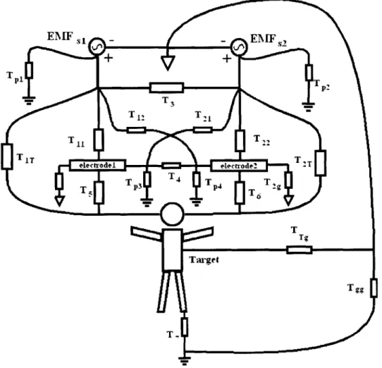
Dielectric Reluctance Model
In Section 2.3.1, the lumped element circuit model of the lamp sensor and target system consisted of capacitances. In the capacitive model, the signal sources were voltage sources
and the signals in the circuit elements were currents. We would like to develop some intuition about the behavior of the system with respect to how it measures changes in the electric fields. Therefore, it will also be useful to build a lumped element circuit model in which the signals in the circuit are electric flux. To quantify the behavior of electric flux below the lamp, we introduce a quantity called dielectric reluctance, T, which acts on electric flux as an impedance acts on current.
The dielectric reluctance between conductors a an b, Tab, is the ratio of the electromotive
force (EMF) between two conductors, Eab to the electric flux coupling the two conductors,
4'e,ab-Tab Eab (2.25)
De,ab
Casting this definition in terms of capacitance by recognizing EMF to be equivalent to voltage,
Qa,b = Eab De,ab (2.26)
Qa,b = CabVab (2.27) Tab = EabVab (2.28) Qa,b (2.29) If follows that Tab ab(2.30) Cab
So that dielectric reluctance as defined above is the ratio of the permittivity of the space between the two conductors to the capacitance between them. For a fixed operating fre-quency, this quantity will be directly proportional to the capacitive impedance magnitude,
1
|Ze| - . (2.31)
WC*
An analogy can be drawn between the EMF source and dielectric reluctance system and a simple voltage source and resistance system. In this analogy, electric-flux becomes
current and dielectric reluctance becomes resistance.
- - i (2.32)
T --+ R, (2.33)
where the exponential term represents the phase shift from the current to the electric flux.
Also, in this analogy, voltage remains as voltage because the analogous quantity 8
ab
will be
Sab = TabPe,ab (2.34)
Cab Qa,b (2.35)
Cab Eab
Using the definition of capacitance, the EMF becomes voltage:
C = -(2.36)
Sab Vab, (2.37)
which is simply a consequence of the fact that EMF is physically indistinguishable from voltage. It is important not to confuse the current i in this analogy with the real measured current from (2.11) in the capacitive model. Because the current in this analogy represents electric flux, there is a 900 phase shift between it and the real current in the capacitive model
and they cannot be the same quantity.
The full dielectric reluctance circuit model is shown in Figure 2-10. In this model, all of the capacitances are replaced with dielectric reluctances according to (2.30) while the voltage sources are replaced with EMF sources. The electric flux signals act on dielectric reluctances as currents do on impedances.
EMIF S1 - _ EAMF, TT TT TI 11 1 T T electrodel electrode2 -T T 3 T 4 T T'1 tzzz Tg TaTroar T~~ Tage T .
Figure 2-10: A lumped element dielectric reluctance model of the lamp sensor and target system.
Chapter 3
Signal Conditioning
In Chapter 2, the lamp was considered as an ac electrical signal source. A lumped element circuit was derived that models the behavior of the electric fields below the lamp in re-sponse to the conducting target. The next task is to design electronics to condition a signal from the lumped element circuit to detect the conducting target. The interface between the lumped element circuit and the signal conditioning electronics is the measurement elec-trodes placed in front of the lamp.
Detection is approached by measurement of differential signals in a nullable, balanced capacitive bridge. Because the nulling is capacitive and based on the geometry of sensing, as opposed to nulling at an op-amp summing junction, it is noise-free. Measuring changes in capacitances below the lamp as deviations from the nulled output has the advantage that the front-end amplifier can have very high gain without saturating its output in the absence of a detection. More subtly, a differential measurement of the electric fields below the lamp eliminates the need for a well-controlled dc voltage reference for detection. The output of the ballast is isolated so that there is theoretically no dc path from the output of the ballast to ground and ac impedances to ground are not controlled, therefore, the potential differences between the bulb surface and for instance, the grounded backplane of the lamp are not predictable.
The solution to the problem of not having a well-controlled voltage reference is an important innovation. The fact that the system is designed to be independent of any absolute ground reference is extremely advantageous for capacitive sensing applications. The only
ground reference that sensing will depend on is the inherent incremental source ground at the center of the lamp source. Particular advantages include that common-mode variations in the ground reference and reactive ground loops can be ignored, and that the target need not be coupled to earth ground in order to be detected.
The topology remains fully differential until digitization because this has the advantage of rejecting common-mode pick-up from interfering signals including 60 Hz ac from the utility power line within the signal conditioning electronics. Also, current-mode detection was chosen because it is insensitive to stray shunt capacitances at the measurement elec-trodes. Therefore, the front-end amplifier is a fully differential transimpedance amplifier for current-mode sensing.
The signal conditioning circuitry consists of the front-end amplifier, a synchronous demodulator, and an analog-to-digital interface. The basic operating principles include current-mode sensing to measure the electric flux at the measurement electrodes, and syn-chronous detection. This chapter concludes with a discussion of the noise sources which ultimately limit the detection range and resolution of the lamp sensor.
In summary, the important contributions and innovations presented in this Chapter are as follows. Sensing signals are conditioned from a nullable capacitive bridge. Nulling the output allows for a large differential gain in the front-end amplifier and the nulling is noiseless because it is capacitive and based on the geometry of the sensor. The differential measurement also removes the necessity for a well-controlled dc voltage reference which may be prone to uncontrolled voltage variations with respect to the alternating bulb surface potential. Finally, synchronous detection of the lamp signal provides insensitivity to stray signals.
3.1 Differential Transimpedance Front-End Amplifier for
Current-Mode Detection
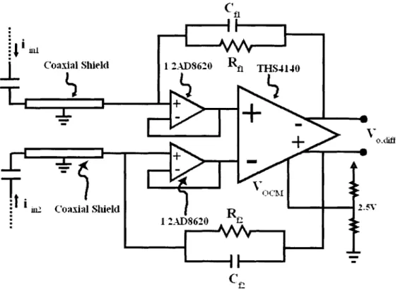
A schematic of the fully-differential front-end amplifier is shown in Figure 3-1. The fully
This part was chosen for its sufficiently high Gain-Bandwidth (GBW) product of 150 MHz and for its dual-rail supply voltage capability. The front-end amplifier incorporates two
JFET buffer amplifiers as the Analog Devices part AD8620[36]. This JFET op-amp was
chosen to have very low input-referred current noise, as will be discussed in Section 3.4, and to have very low input bias current. Because the front-end amplifier will need to have a very large transimpedance in order to measure the small current signals, any differential input bias current to the input terminals of the amplifier (input offset current) will result in a relatively large output differential offset voltage. Consequently, a JFET input buffer is used to buffer the inputs to the op-amp which has a low input bias current of approximately
130 pA and more importantly, a low input offset current of approximately 20 pA[36].
Consider, for instance, a feedback impedance of 1 MQ which roughly corresponds to a differential transimpedance of I MQ. If the inputs to the fully-differential amplifier were left unbuffered, the typical input offset current taken from the data sheet for the THS4140 of 0.lpA would result in a differential output voltage offset of lOOmV. With the inputs buffered with the JFET AD8620 amplifiers, the differential output voltage offset will be
nominally, 20 pV[3 6].
Also, the connection between the measurement electrode and the input to the tran-simpedance amplifier is made with shielded coaxial cables. The shields are connected to ground so that the connection is shielded from electric interference. The coaxial shield capacitance to ground is a significant capacitance in the stray capacitance from the
mea-surement electrodes to ground, i.e. Cp3,4 from Section 2.3, however, as will be shown in
Chapter 4, these stray capacitances will not affect the closed-loop output response.
Finally, the THS4140 uses common-mode feedback so that the output common-mode voltage is constant. This voltage is set to 2.5V with a resistor divider so that the common-mode input voltage to the Analog-to-Digital Converter (ADC) will be centered between its
4'l
Coaxial Shield 1 2AD8620 Rfi THS4140
i2 Coaxial Shield
12-ADS620 f2
Figure 3-1: Schematic of the Low-Noise Analog Front-End Amplifier.
3.1.1
Differential Front-End Operating Principles
The lamp sensor electronics are implemented with a fully differential topology for the sig-nal conditioning circuitry, meaning that the inputs and outputs of each stage are differential.
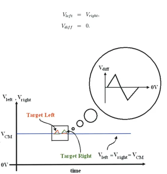
One advantage of the fully differential topology is that it rejects common-mode interfer-ence. Interfacing the differential measurement with the balanced or symmetric capacitive bridge formed by the capacitances below the lamp has the advantage that the front-end am-plifier can have very high gain without saturating its output. This is because in a balanced bridge, the no-detection case corresponds to zero differential output voltage. Then, the very high gain can be used to amplify small deviations in the electric flux measurements amidst large nominal or common-mode electric flux magnitudes. Figure 3-2 illustrates the general principle of detecting small signal deviations amidst large common-mode nominal signals with a differential measurement. Keeping in mind that in the figure,
so that when Vieft ,Vri CM oV- -'%diff ght Target Left
I-ko
_'ATai-get Right Vleft =right=CM
time
Figure 3-2: The concept of separating differential-mode signals from common-mode sig-nals.
In addition to separating differential signals from common-mode signals, it is important to understand how the front-end amplifier measures current at the measurement electrodes. To see how the current-mode measurement takes place, it is argued that the differential-mode input voltage at the input terminals of the amplifier is essentially zero. This argument is similar to the argument for a more common single-ended op-amp in a negative feedback configuration like that shown in Figure 3-3.
Because the response of the op-amp to input voltages is
Vout = A(v+ - v_) (3.4) Vie ft Vdif f = Vright, =0. (3.2) (3.3)
f
V il
-out
in+
Figure 3-3: A typical op-amp negative feedback connection
and A is very large, any differential input voltage v+ - v_ results in a large output voltage
Vout. If there is a positive differential input voltage, i.e.
v+ > v_, (3.5)
the output voltage increases so that the inverting terminal voltage increases, thus decreas-ing the differential input voltage. If there is a negative differential input voltage the output voltage decreases so that the inverting terminal voltage decreases, thus decreasing the dif-ferential input voltage. The result is that the difdif-ferential input voltage is always nearly OV. In other words, the two input terminal voltages are nearly equal.
This reasoning can be extended to the fully differential amplifier, as in Figure 3-4 for which the open-loop gain is differential:
Av,_ Vod (3.6)
Vin,d
Now, a differential input voltage increases the differential output voltage. The negative feedback in the fully differential case is implemented so that the inverting output terminal feeds back to the non-inverting input terminal and the non-inverting output terminal feeds back to the inverting input terminal. Increasing the differential input voltage increases the differential output voltage and causes the input differential voltage to decrease. Therefore the differential input voltage is always nearly 0 V. In other words, the two input terminal voltages are nearly equal.
Zf
Figure 3-4: Differential input current in a differential amplifier
In the context of current-mode detection, the differential transimpedance amplifier draws a differential current at its input such that its input terminal voltages remain equal. For an
ideal amplifier with infinite open-loop gain (A -+ oc), the differential amplifier has a
dif-ferential transimpedance, Zd equal to the impedance of the feedback impedance formed by
the parallel combination of Rf and Cf,
Zd(s) = Z(= Rf (3.7)
RfsC + 1
Therefore, in the negative feedback connection, the fully differential transimpedance
amplifier in Figure 3-4 measures a differential input current iin,d and multiplies it by the
differential transimpedance Zd(s) so that the output is
Vo,d = i (3.8)
where
iin,d = iinl - iin2. (3.9)
3.1.2
Differential Transimpedance Amplifier Input Characteristics
The impedances presented by the capacitances in the lumped element capacitance model of Chapter 2 are relatively large. A nominal value for the capacitance between the
sig-nal source and the measurement electrode in front of that source is 1 pF. With the ballast operating frequency of 42 kHz, the capacitive impedance is
1
=Zcj)| = 3.79 MQ. (3.10)
WC
Nominal values of the capacitive impedance between the source and the target are gen-erally even larger. For a capacitance of 10 fF, the impedance is 379 MQ. The front-end amplifier should be able to accurately sense the small current signals in the capacitive cir-cuit. There are two input characteristics of the front-end amplifier that make it appropriate for accurate current-mode measurement. First, very little current should be lost to the input terminals of the op-amp or any shunt impedance at the measurement nodes in the front-end amplifier. Second, the differential input impedance of the front-end amplifier should be very small.
To see that very little current is lost to the input terminals of the op-amp, consider the effect of the shunt impedance at the measurement node on the differential output voltage in Figure 3-5. In current-mode detection, the measurement electrode is connected directly to the input terminal of the high gain operational amplifier.
Zf
2
1iZ
Zf
Figure 3-5: A fully differential amplifier taking into account shunt impedances from the measurement nodes to incremental ground.
The shunt impedance, Zeh, represents both the op-amp input terminal impedance and