HAL Id: hal-01612502
https://hal.laas.fr/hal-01612502
Submitted on 6 Oct 2017
HAL is a multi-disciplinary open access
archive for the deposit and dissemination of
sci-entific research documents, whether they are
pub-lished or not. The documents may come from
teaching and research institutions in France or
abroad, or from public or private research centers.
L’archive ouverte pluridisciplinaire HAL, est
destinée au dépôt et à la diffusion de documents
scientifiques de niveau recherche, publiés ou non,
émanant des établissements d’enseignement et de
recherche français ou étrangers, des laboratoires
publics ou privés.
Stéphane Calvez, Gael Lafleur, Alexandre Larrue, Pierre-François Calmon,
Alexandre Arnoult, Guilhem Almuneau, Olivier Gauthier-Lafaye
To cite this version:
Stéphane Calvez, Gael Lafleur, Alexandre Larrue, Pierre-François Calmon, Alexandre Arnoult, et
al.. Vertically Coupled Microdisk Resonators Using AlGaAs/AlOx Technology. IEEE Photonics
Technology Letters, Institute of Electrical and Electronics Engineers, 2015, 27 (9), pp.982 - 985.
�10.1109/LPT.2015.2405031�. �hal-01612502�
Abstract— In this letter, we report the first experimental demonstration of micro-disk resonators that are vertically-coupled to their buried access waveguides on III-V semiconductor epitaxial structures using an original fabrication process. The here-proposed and validated three-dimensional integration scheme exploits selective lateral thermal oxidation of aluminium-rich AlGaAs layers. Compared to the previously reported processing techniques, this new scheme is simpler as it does not require any planarization or substrate transfer steps. As a proof-of-principle demonstration of this approach, 250 µm-diameter micro-disk devices exhibiting quality factor reaching ~8500 have been successfully fabricated.
Index Terms— Monolithic integration, optical resonator, vertical coupling, AlOx, oxidation, GaAs, whispering gallery modes
I. INTRODUCTION
NTEGRATED whispering gallery mode (WGM) resonators in the form of micro-ring, micro-disk or micro-racetrack resonators have attracted a lot of attention since they can provide large field enhancement in a compact format and, thereby, enable the fabrication of selective filters, low-threshold emitters, high-speed modulators, sensitive optical sensors or nonlinear converters [1][2][3]. Many of these applications would benefit from the resonator and the light source being integrated on the same chip, i.e. being made of III-V semiconductors. Furthermore, irrespective of the targeted application, the resonators require to exhibit high quality factors which, in turns, leads to two technological challenges: (1) limiting the amount of scattering loss along the resonator periphery and (2) accurately controlling the input/output coupling rate(s) between the resonator and its access waveguide(s). Since light is usually coupled in and out
Manuscript received October 10, 2014; accepted. Date of publication ; date of current version 02/02/2015.
This work has been supported by the Centre National d’Etudes Spatial (CNES).
S. Calvez, G. Lafleur, A. Larrue, P.-F. Calmon, A. Arnoult, G. Almuneau and O. Gauthier-Lafaye are with CNRS, LAAS, 7 avenue du colonel Roche, F-31400 Toulouse, France and with Univ de Toulouse, UPS, LAAS, F-31400 Toulouse, France (e-mail: [email protected])
A. Larrue is now with III-V Lab, Campus de Polytechnique, 1, avenue Augustin Fresnel , RD128, F-91767 Palaiseau Cedex (e-mail:
.
of the resonators by evanescent coupling, the preferred technique to address the latter challenge relies on using a vertical integration scheme where the access waveguide lies (typically) below the resonator. Indeed, this approach offers greater fabrication tolerances and enables different materials to be used for the resonator and its access waveguides [4]. However, it generally suffers from complex fabrication procedures involving either a demanding planarization of the coupling layer to a set thickness [5],[6],[7] or a critical substrate transfer to allow both sides of a few-micrometer-thick epilayer to be processed [8].
In this letter, we report the first use of III-V semiconductor/oxide technology to fabricate, using a simple process, monolithically-integrated micro-disk resonators which are vertically-coupled to buried oxide-confined access waveguides. This work, largely inspired by silicon photonic integrated circuits made by the SIMOX process [9], exploits the use of the selective lateral oxidation of high-aluminium containing layers (AlGaAs here) and its associated refractive index change (nAlOx~1.6, nAlGaAs~3.2) to create a controlled
optical confinement at depth i.e. a 3D optical structuration compatible with high-confinement [10] and low-loss propagation [11]. Furthermore, as for Vertical-Cavity Surface-Emitting Lasers, the AlOx technology can be used to induce not only optical confinement but also electrical confinement, and thereby opens an avenue towards the monolithic integration of WGM resonators with active III-V multi-functional photonic components and, in particular, with laser sources.
II. DEVICE DESIGN
The device design consists in a buried oxide-confined rib waveguide that is vertically-coupled to a GaAs-based micro-disk resonator (see Fig. 1 and 2). The multi-layer epitaxial stack is based on AlxGa1-xAs alloys and is presented in Fig. 3.
The waveguide claddings (Al0.7Ga0.3As and Al0.3Ga0.7As) were
chosen to be asymmetric such that a greater field penetration occurs towards the resonator. The 716 nm-thick resonator/waveguide coupling region includes two 68 nm-thick Al0.98Ga0.02As layers to be laterally oxidized, sandwiched
between three Al0.3Ga0.7As layers. The partial oxidation of
these layers will form oxide-apertured stripes and thus induce lateral waveguiding. The upper layer (located at 100 nm beneath the disk core) is also used to increase the vertical
Vertically-coupled micro-disk resonators using
AlGaAs/AlOx technology
S. Calvez, G. Lafleur, A. Larrue, P.-F. Calmon, A. Arnoult, G. Almuneau and O. Gauthier-Lafaye
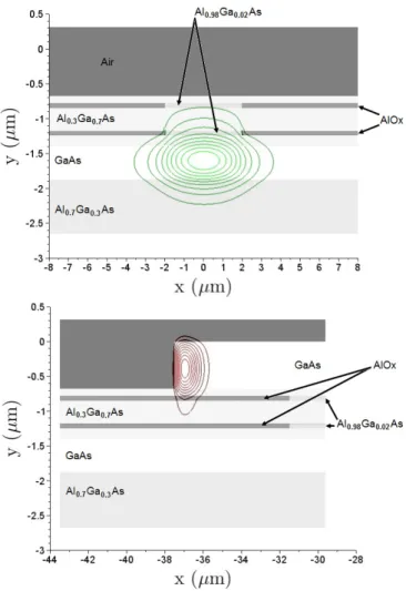
was positioned relatively far (150-nm-away) from the GaAs-based core of the access waveguide to provide single-mode operation for (weakly-confined (Δn~10-2)) large-width modes, thereby reducing the dependence on lateral offset of the waveguide/resonator coupling. The (0.68 µm) thickness of the GaAs-core resonator was also set to support vertically only the quasi-TE fundamental mode. Structures with oxide apertures smaller than 4 µm were calculated using finite difference modelling [12] to exhibit single lateral mode propagation (see Fig. 3).
III. DEVICE FABRICATION
The AlGaAs (vertical) structure was grown on a (100) GaAs substrate by molecular beam epitaxy (Riber 412). The wafer was post-processed using two photolithography steps using direct laser writing (Heidelberg DWL 200) and SPR700 photoresist. The first mask level is used to define the oxidation mesa which, upon oxidation, will lead to the access waveguides (oriented 7° off the normal to the cleaved facet
mode. The second mask level defines the resonators which were nominally positioned to have the maximum field intensity aligned with the center of the access waveguides. The re-alignment accuracy was estimated to be better than 0.5 µm. These patterns were transferred sequentially in the AlGaAs stack by an ICP-RIE plasma etch using a Cl2/N2/Ar
gas mixture and the etch depth (respectively of 1740 nm and 720 nm) was monitored by optical reflectometry. The top image of Fig. 1 highlights the resulting 3D mesa structure. Simultaneous wet thermal oxidation of both Al0.98Ga0.02As
layers was carried out in a custom furnace with in-situ spectrally-resolved optical monitoring [13]. During the oxidation, the sample was held at a substrate temperature of 400°C, in a reduced pressure environment (~0.5 atm.), and exposed to a mixed H2/N2/H2O gas steam generated by an
evaporator-mixer system at 95°C. The oxidation front progressed linearly at a rate of 0.11 µm/min from the edges of the oxidation mesa and was stopped when the oxide aperture width reached the nominal value of 3.5 µm and the oxide penetration from the micro-disk edges was of 6 µm. Both the bottom picture of Fig. 1 and Fig. 2 and indicate the obtained Al0.98Ga0.02As/AlOx in-plane distribution. The samples were
then back-polished down to a substrate thickness of ~150 µm, cleaved to be 1200 µm-long and mounted on Si sub-mounts. It should be emphasized that none of the technological steps use in the above-described process was specifically optimized to create low-loss structures.
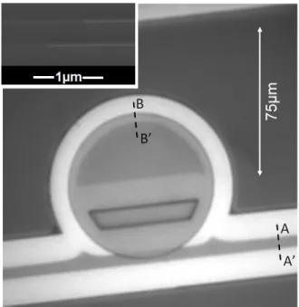
Fig. 2 shows a top-view near-infrared optical microscope image of one of the fabricated micro-disks. We observed that the oxidation depths of the two AlGaAs layers are actually not
Fig. 1. Colorized tilted SEM pictures of a 75 µm-diameter micro-disk vertically coupled to a buried oxide access waveguide. The upper image highlights the vertical topography of the device whilst the lower image shows the buried AlGaAs/AlOx lateral distribution.
Fig. 2. Near-infrared (λ=770 nm) microscope image of a fabricated 75 µm-diameter micro-disk vertically coupled to a buried oxide access waveguide. The dashed lines indicate where the cross-sectional modes profiles of Fig. 2 were calculated. Inset: SEM cross-section of the two oxidized Al0.98Ga0.02As
strictly identical, a phenomenon we believe to be the result of oxide-induced strain distribution in the asymmetric vertical structure [14]. The bottom waveguide aperture width was measured to be ~3.7 µm by using a focused ion beam (FIB) and scanning electron microcopy (SEM) characterizations, while the upper confining layer aperture width was found to be ~1.2 µm larger.
IV. DEVICE CHARACTERISATION
The device optical characteristics were measured using a step-tunable laser with central wavelength of 1.6 µm, a 10 pm spectral resolution and a 100 kHz linewidth. Light injection through the cleaved facets was performed using a lensed fibre and the transmitted light was collected and optically relayed to another single-mode fibre. First, the losses of straight waveguides (whose propagation direction is orthogonal to the cleavage planes) were found to be ~2.5cm-1 using standard Fabry-Perot analysis, on a par with other low-loss AlOx/GaAs waveguides [11]. Subsequently, the transmission spectra of the resonators with diameter of 75- and 250-µm were recorded and are shown on Fig. 4. These curves are as expected with resonances separated by 3.07 and 0.91 nm respectively corresponding to group indices of 3.539 and 3.601. Lorentzian
fitting of the presented resonance dips reveals that the largest device exhibits Q factors of 8546 ± 994. The 75 µm micro-disk transmission spectrum shows two sets of resonances corresponding respectively to the first and second order lateral modes of the micro-disk and whose respective Q factors are 4610 ± 374 and 2942 ± 417. Analysing these spectra using the micro-disk general transmission formula [15] and taking into account that the devices are operated in the over-coupling regime by design (because of the relatively thin AlGaAs separating layer and because the effective index in the microdisk is slightly higher than in the buried waveguide), the intensity loss coefficients in the disk are found to be 4.8±0.8 and 5.7±1.8 cm-1 (equivalent to intrinsic Q factors of Q0~30200 and 25400) and the amplitude coupling coefficients
are inferred to be 68.4 and 79.7% respectively for the 75- and the 250-µm-diameter resonators. The independence of the extracted loss value to the diameter is attributed to the fact that sidewall-roughness-induced loss is the dominant loss process here and that the contribution of the bending loss is negligible for these large-diameter disks. Using a refined process like the one reported in [16], a reduction of this loss value down to ~0.3 cm-1 can be anticipated. Optimization of the thickness of the separating Al0.3Ga0.7As layer and of the
access-guide-to-disk lateral offsets should also allow the critical coupling condition to be reached, in which case the expected Q factors would then be of 2.4 105, on a par with the results achieved in [10][17].
V. CONCLUSION
In conclusion, a novel fabrication procedure to make micro-disk or micro-ring resonators that are vertically-coupled to buried oxide access waveguides using AlGaAs/AlOx technology has been established. The samples resulting from the first fabrication run exhibits Q factors up to 8500. Future work will include an optimization of the geometry and fabrication to improve the performance of the devices and will aim to further explore the potential of the here-introduced
3-Fig. 3. Calculated profiles for the fundamental TE-like modes of (a) 4 µm-wide access waveguide (cross-section A-A’ on Fig. 1) and (b) a 75-µm diameter micro-disk (cross-section B-B’on Fig. 1)[1],[12].
Fig. 4. Transmission characteristics of 75- and 250-µm-diameter micro-resonators.
platforms.
ACKNOWLEDGEMENTS
The authors would like to acknowledge that this work was partly supported by the Centre National d’Etudes Spatial (CNES) and the French RENATECH network of micro-fabrication facilities.
REFERENCES
[1] A. B. Matsko and V. S. Ilchenko, “Optical resonators with whispering gallery modes I: basics,” IEEE J Sel Top Quantum Electron, vol. 12, no. 1, pp. 3–14, 2006.
[2] S. Feng, T. Lei, H. Chen, H. Cai, X. Luo, and A. W. Poon, “Silicon photonics: from a microresonator perspective,” Laser Photonics Rev., vol. 6, no. 2, pp. 145–177, Apr. 2012.
[3] J. Ward and O. Benson, “WGM microresonators: sensing, lasing and fundamental optics with microspheres,” Laser Photonics Rev., vol. 5, no. 4, pp. 553–570, Jul. 2011.
[4] M. Ghulinyan, F. Ramiro-Manzano, N. Prtljaga, R. Guider, I. Carusotto, A. Pitanti, G. Pucker, and L. Pavesi, “Oscillatory Vertical Coupling between a Whispering-Gallery Resonator and a Bus Waveguide,” Phys. Rev. Lett., vol. 110, no. 16, p. 163901, Apr. 2013.
[5] S. Suzuki, K. Shuto, and Y. Hibino, “Integrated-optic ring resonators with two stacked layers of silica waveguide on Si,” Photonics Technol. Lett. IEEE, vol. 4, no. 11, pp. 1256–1258, 1992.
[6] Y. Kokubun, Y. Hatakeyama, M. Ogata, S. Suzuki, and N. Zaizen, “Fabrication technologies for vertically coupled microring resonator with multilevel crossing busline and ultracompact-ring radius,” IEEE J. Sel. Top. Quantum Electron., vol. 11, no. 1, pp. 4–10, Jan. 2005. [7] M. Ghulinyan, R. Guider, G. Pucker, and L. Pavesi, “Monolithic Whispering-Gallery Mode Resonators With Vertically Coupled Integrated Bus Waveguides,” IEEE Photonics Technol. Lett., vol. 23, no. 16, pp. 1166–1168, Aug. 2011.
[8] P. P. Absil, J. V. Hryniewicz, B. E. Little, F. G. Johnson, K. J. Ritter, and P.-T. Ho, “Vertically coupled microring resonators using polymer wafer bonding,” Photonics Technol. Lett. IEEE, vol. 13, no. 1, pp. 49– 51, 2001.
[9] P. Koonath, T. Indukuri, and B. Jalali, “Vertically-coupled micro-resonators realized using three-dimensional sculpting in silicon,” Appl. Phys. Lett., vol. 85, no. 6, p. 1018, 2004.
[10] E. Peter, I. Sagnes, G. Guirleo, S. Varoutsis, J. Bloch, A. Lemaı^tre, and P. Senellart, “High-Q whispering-gallery modes in GaAs∕AlOx microdisks,” Appl. Phys. Lett., vol. 86, no. 2, p. 021103, 2005. [11] C. Ozanam, M. Savanier, L. Lanco, X. Lafosse, G. Almuneau, A.
Andronico, I. Favero, S. Ducci, and G. Leo, “Toward an AlGaAs/AlOx near-infrared integrated optical parametric oscillator,” J. Opt. Soc. Am. B, vol. 31, no. 3, pp. 542–550, Mar. 2014.
[12] A. B. Fallahkhair, K. S. Li, and T. E. Murphy, “Vector Finite Difference Modesolver for Anisotropic Dielectric Waveguides,” J. Light. Technol., vol. 26, no. 11, pp. 1423–1431, Jun. 2008.
[13] G. Almuneau, R. Bossuyt, P. Collière, L. Bouscayrol, M. Condé, I. Suarez, V. Bardinal, and C. Fontaine, “Real-time in situ monitoring of wet thermal oxidation for precise confinement in VCSELs,” Semicond. Sci. Technol., vol. 23, no. 10, p. 105021, Oct. 2008.
[14] F. Chouchane, G. Almuneau, N. Cherkashin, A. Arnoult, G. Lacoste, and C. Fontaine, “Local stress-induced effects on AlGaAs/AlOx oxidation front shape,” Appl. Phys. Lett., vol. 105, no. 4, p. 041909, Jul. 2014.
[15] A. Yariv, “Universal relations for coupling of optical power between microresonators and dielectric waveguides,” Electron. Lett., vol. 36, no. 4, pp. 321–322, 2000.
[16] G. A. Porkolab, P. Apiratikul, B. Wang, S. H. Guo, and C. J. K. Richardson, “Low propagation loss AlGaAs waveguides fabricated with plasma-assisted photoresist reflow,” Opt. Express, vol. 22, no. 7, pp. 7733–7743, Apr. 2014.
quantum boxes,” Appl. Phys. Lett., vol. 75, no. 13, pp. 1908–1910, 1999.