Building Efficient Light-Matter Interfaces for
MA
Quantum Systems
by
Tsung-Ju Jeff Lu
ARCHIVES
SSACHUSETTS INSTITUTE OF TECHNOLOGYNOV 0 2 2015
LIBRARIES
B.S. Electrical Engineering, California Institute of Technology (2013)
Submitted to the Department of Electrical Engineering and Computer
Science
in partial fulfillment of the requirements for the degree of
Master of Science in Electrical Engineering and Computer Science
at the
MASSACHUSETTS INSTITUTE OF TECHNOLOGY
September 2015
@
Massachusetts Institute of Technology 2015. All rights reserved.
Author
....
Signature redacted
Depart(ent oiElectrifal Engine1ering and Computer Science
August 28, 2015
Cetfidby..Signature
redacted
Certified by.
.
...
Dirk R. Englund
Assista t Pro ssor of Electrical Engineering
Thesis Supervisor
Accepted by....Signature
redacted
/
0 Wofessor Leslie A. Kolodziejski
Chair of the Committee on Graduate Students
Building Efficient Light-Matter Interfaces for Quantum
Systems
by
Tsung-Ju Jeff Lu
Submitted to the Department of Electrical Engineering and Computer Science on August 28, 2015, in partial fulfillment of the
requirements for the degree of
Master of Science in Electrical Engineering and Computer Science
Abstract
Efficient collection of photons from quantum memories, such as quantum dots (QDs) and nitrogen vacancy (NVs) centers in diamond, is essential for various quantum technologies. This thesis describes the design, fabrication, and utilization of novel photonic structures and systems to achieve potentially world-record photon collection from quantum dots. This technique can also be applied to NVs in diamond in the near future.
Also, the NV- charged state has second-scale coherence times at room tempera-ture that make it a promising candidate for solid state memories in quantum
com-puters and quantum repeaters. NV- is an individually addressable qubit system
that can be optically initialized, manipulated, and measured. On-chip entanglement generation would be the basis of scalability for quantum information processing tech-nologies. These properties have enabled recent demonstrations of heralded quantum entanglement and teleportation between two separated NV centers. To improve the entanglement probability in such schemes, it is imperative to improve the efficiency with which single photons from a NV center can be guided into a low-loss single-mode waveguide. As such, a second component of this thesis focuses on the development of a photonic integrated circuit based on aluminum nitride that would incorporate pre-selected, long-lived NV center quantum memories as well as pre-selected, high-performance superconducting nanowire single-photon detectors (SNSPDs). This hy-brid device would have the capability to perform on-chip entanglement of photons from separate quantum memories to build up a quantum repeater necessary for long-distance quantum communication and distributed quantum computing.
Thesis Supervisor: Dirk R. Englund
Acknowledgments
This thesis would not have been possible without the guidance of many people. First of all, I would like to acknowledge my advisor, Professor Dirk Englund, for his guid-ance and support. It has been a real privilege to work with Professor Englund, learning directly from him, and always being able to ask him for advice on anything. He has played such a large role in shaping my academic and research interests and helping me reach my goals that I would like to thank him for that.
I would also like to thank everyone in the Quantum Photonics Laboratory for their
help in everything. I have truly learned so much in the past two years from everyone in the group. I feel like I am a better researcher and person as a result. It is amazing to work with this group of highly intelligent and extremely motivated academics. It is really a blessing to be in such a wonderful work environment. I particularly want to thank Dr. Gabriele Grosso for helping me with the fiber-integrated single photon source project in this thesis. He worked with me on building the optical setup and mentored me in doing the spectroscopy experiments.
Also, I would like to thank my collaborators Ryan Camacho, Matt Eichenfield, Ian Frank, and Jeremy Moore from Sandia National Laboratories. Although I only visited for one week, it was a great experience to see what it was like to work in a national lab. I appreciated all of you making me feel welcomed. I enjoyed Albuquerque very much and look forward to visiting more in the future for our collaboration.
In addition, I would like to thank Jim Daley and Mark Mondol of NanoStructures Laboratory for all their help and expertise in fabrication. Furthermore, I would like to thank Eric Lim, Dave Terry, Bob Bicchieri, and the rest of Microsystems Technology Laboratories for all their help and expertise in fabrication as well. Developing a reliable fabrication process was a difficult part in this Master's Thesis, so I am grateful to all these people for helping me with this huge obstacle.
Finally, I want to give my utmost thanks to my mother and father for their love, care, and countless sacrifice they have made for my education. They have been my guiding light in every difficult and important decision throughout my life. They are
very supportive in everything I do, and I live to make them proud. Thank you so much for being the best parents imaginable.
Contents
1 Introduction
1.1 Self-assembled semiconductor quantum dots . . . .
1.1.1 Progress and Challenges of Using Epitaxial Quantum Dots . .
1.2 Nitrogen Vacancy Center in Diamond . . . . 1.2.1 NV- defect center . . . . 1.3 Thesis O utline . . . .
2 Fiber-Integrated Single Photon Source
2.1 Motivation and Goals . . . . 2.2 Bullseye Grating Structure . . . . 2.2.1 Previous Studies . . . . 2.2.2 Pick-and-Place Method . . . . . 2.2.3 Modifications in Structure . . . 2.3 Fabrication . . . . 2.4 Experimental Results . . . . 2.4.1 Optical Setup . . . . 2.4.2 Spectroscopy Experiments . . .
3 Quantum Repeater using NV and Nanophotonic Processor
3.1 Overview and Vision ...
3.2 Aluminum Nitride . . . .
Wide-Bandgap Programmable
37 . . . . 37 . . . . 39
3.2.1 Sandia National Laboratories' AlN Fabrication Process
17 17 20 20 20 22 23 . . . . 23 . . . . 24 . . . . 24 . . . . 2 4 . . . . 2 5 . . . . 2 8 . . . . 30 . . . . 30 . . . . 33 39
3.3 Mask Patterns for Sandia Process . . . . 4 Passive Components of Aluminum Nitride Photonic
cuit
4.1 Adiabatic Waveguide Taper . . . .
4.2 Bragg Grating Filter . . . . 4.3 Disk Resonator . . . .
4.3.1 Dependence on Coupling Gap . . . .
4.3.2 Dependence on Coupling Length . . . .
4.3.3 Plans for Better Design . . . . 4.4 Directional Coupler for 50:50 Split . . . .
4.4.1 Analytical Calculations . . . . 4.4.2 Variational FDTD Simulations . . . . 4.4.3 3D FDTD Simulations . . . . 5 In-5.1 5.2 5.3 41 Integrated Cir-49 49 50 54 54 57 60 61 61 63 65 69 70 71 72 76 76 78 81
House Fabrication and Fast Prototyping
First Generation Test Structures . . . .
5.1.1 Grating Couplers . . . .
Fabrication . . . .
Experimental Results . . . .
5.3.1 Confocal Setup . . . .
5.3.2 Confocal Microscopy Experiments . . . .
List of Figures
1-1 Simplified depiction of the excited electron and the hole in an exciton entity and the corresponding energy levels. The total energy is the sum of the band gap energy between the occupied level and unoccupied energy level, the en-ergy involved in the Coulomb attraction in the exciton, and the confinement energies of the excited electron and the hole [24]. . . . . 18
1-2 Schematic of the nitrogen vacancy center in the diamond lattice. . . . . . 21
2-1 (a) Pick-and-place membrane transfer of an SNSPD onto a waveguide. (b) Suspended SNSPD membrane. (c) SNSPD membrane that was removed from the carrier chip using a tungsten microprobe with a drop of hardened PDMS at the tip. (d) SNSPD membrane integrated to a silicon waveguide
[151 . . . . 24
2-2 (a) Modification of bullseye structure for completely suspended structures.
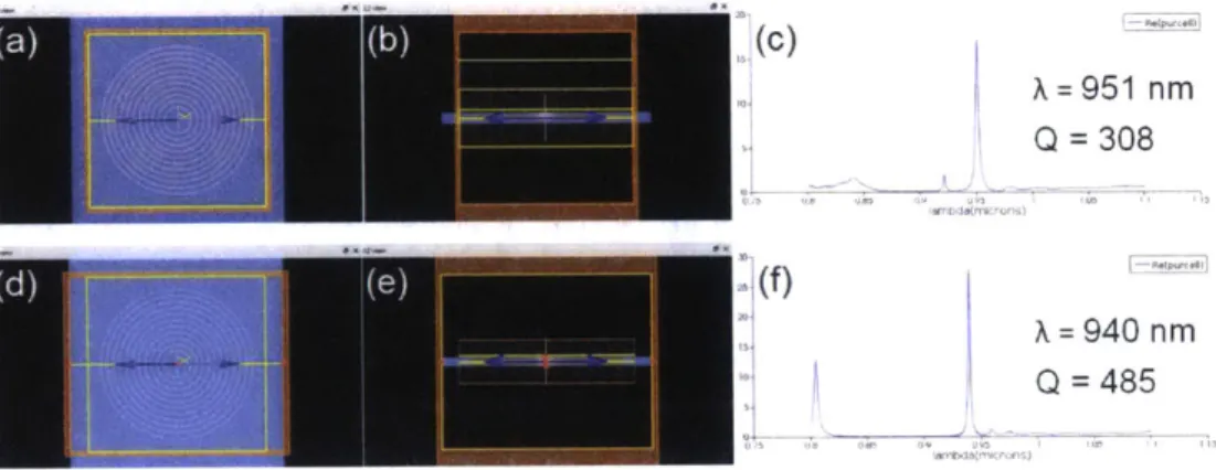
2-3 This is a comparison using the FDTD software Lumerical to see the difference between the original partial etch bullseye structure in Davanco et al. and the full etch modified bullseye structure we developed. For these simulations, the quantum dot dipole was assumed to be oriented along the xy plane, which means only the TE slab waves were excited. (a) and (b) show the simulation layout of partial etch bullseye structure, with a quantum dot dipole placed at the center of the structure. (c) Purcell enhancement spectrum associated with (a) and (b), which shows that the resonant wavelength is 951 nm and
Q
is 308. (d) and (e) show the simulation layout of the modified bullseye structure with suspension bridges to hold the structure when the trenches are fully etched, with a quantum dot dipole placed at the center of the structure. (f) Purcell enhancement spectrum associated with (d) and (e), which shows that the resonant wavelength is 940 nm andQ
is 485. .... 262-4 (a) and (b) show the simulation layout of the complete bullseye membrane on top of a fiber facet system. (b) Electric field intensity in the xy plane. (c) Far-field polar plot of the cavity mode. (d) Purcell enhancement spectrum, which shows that the resonant wavelength of the entire system is 945 nm and
Q
is 358. . . . . 27 2-5 This is a comparison using the FDTD software Lumerical to see the differencebetween the original partial etch bullseye structure in Davanco et al. (left half) and the full etch modified bullseye structure we developed (right half). The top images are the log scale Electric field intensity of the circular grating structure in the xz plane. The bottom images show the percentage of total emission collected by NA = 0.5 optics as a function of wavelength. .... 28 2-6 Starting substrate of the quantum dot wafers. The InAs quantum dots are
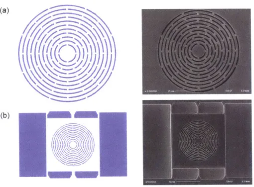
embedded near the center of the GaAs layer. . . . . 28 2-7 (a) Left: design, right: fabricated structures of "bullseye" circular grating (b)
Left: design, right: fabricated structures of "bullseye" circular grating with suspended bridges that can be broken to systematically place the structure on a fiber facet. . . . .. . . . . 30
2-8 4F imaging configuration [101. . . . . 31 2-9 Experimental setup for quantum dot experiments. . . . . 32
2-10 (a) Microscope objective directly over Montana cryostat. (b) Portion of setup that transitions from the elevated optical platform to the optical table. 32
2-11 (a) Confocal scan of the fluorescence of an array of bullseye circular gratings.
(b) Zoomed-in confocal scan of the fluorescence of one bullseye circular
grat-ing. Note: the dimensions on the side are not the actual physical dimensions of the scan, but rather the voltage applied to each galvos mirror. . . . . . 33
2-12 Spectrum of the bulk quantum dots at an unpatterned area. . . . . 34
2-13 Spectrum at the center of a bullseye structure with a bright enhanced
fluo-rescence spot. . . . . 34 2-14 Spectrum at the center of a bullseye structure with a bright enhanced
fluo-rescence spot, using a higher density grating and lower pump power. . . . 35
3-1 Overview of quantum repeater hardware, which uses nitrogen vacancy cen-ters in diamond as quantum regiscen-ters, AlN photonic integrated circuit for dynamic photonic routing, and SNSPDs as on-chip detectors. . . . . 38 3-2 Complete device overview of Sandia National Laboratories' AlN
optome-chanically tunable microdisk that can serve as an optical filter. . . . . 40
3-3 Fabrication process of Sandia National Laboratories' AlN optomechanically tunable microdisk. . . . . 40 3-4 Condensed overview of the mask patterns for each MZI element. All masks
for the 6 layers are overlapped and displayed. . . . . 41
3-5 Top-down view depicting a NV nanobeam cavity membrane integrated to the AlN photonic waveguide network. This also shows the proximity of the microwave striplines with respect to the NV nanobeam cavity. . . . . 43
3-6 Side view depicting a NV nanobeam cavity membrane integrated to the AlN photonic waveguide network. This also shows the proximity of the microwave striplines with respect to the NV nanobeam cavity. . . . . 44
3-7 Top-down view depicting a SNSPD membrane integrated to the AIN pho-tonic waveguide network. The SNSPD gold pads make contact with the gold pads on the chip so that the larger contact pads can be wirebonded to electrically operate the SNSPD. . . . . 44
3-8 Side view depicting a SNSPD membrane integrated to the AlN photonic waveguide network. The SNSPD gold pads make contact with the gold pads on the chip so that the larger contact pads can be wirebonded to electrically operate the SNSPD. . . . . 45
3-9 Mask patterns for making the tunable microdisk. (a) Pattern 1 for the nitride etch in step 2. (b) Pattern 2 for the bottom electrode etch in step 4. (c) Pattern 3 for etching through the AIN and bottom electrode to the tungsten layer in step 9. (d) Pattern 4 for the AlCu etch in step 10. (e) Pattern 5 for etching through the AlN and oxide to the nitride layer in step 12. (f) Overview of the mask patterns for each tunable microdisk. All masks for the 6 layers are overlapped and displayed. . . . . 46
3-10 Mask patterns for making the rest of the MZI. (a) The rest of pattern 5 for
defining the AIN structures. (b) Pattern 6 for the metal liftoff step after step 12. . . . . 47
4-1 Adiabatic waveguide taper for coupling light efficiently from diamond nanobeam cavities to AlN waveguide. This design is taken exactly as-is from Mouradian
et al.'s 2014 paper [141. . . . . 50
4-2 (a) Overall design of Bragg Grating filter, which is used for filtering the 532 nm green excitation laser and allowing the 637 nm NV fluorescence to pass through. (b) Dimensions of the Bragg Grating filter, where the period is 144 nm, the original waveguide width is 400 nm, the corrugated waveguide width is 280 nm, and the thickness of the waveguide is 200 nm. (c) Electric field profile of the larger width 400 nm cross section, which has an effective mode index of 1.89868. (d) Electric field profile of the smaller width 280 nm corrugated cross section, which has an effective mode index of 1.810855. . . 50
4-3 (a) Bandstructure spectrum at the band edge k- = ir/a. (b) Transmission spectrum for 5000 periods. (c) Transmission spectrum for 8000 periods. . 53
4-4 (a) Simulation setup for a disk resonator of 30 pLm coupled to two bus waveg-uides by a coupling length of 12.3890 Rm and coupling gap of 200 nm. The input port is at the top left, the through port is at the top right, and the drop port is at the bottom left. (b) Transmission spectrum of the through port. (c) Transmission spectrum of the drop port. . . . . 55
4-5 (a) Simulation setup for a disk resonator of 30 pm coupled to two bus waveg-uides by a coupling length of 12.3890 pm and coupling gap of 100 nm. The input port is at the top left, the through port is at the top right, and the drop port is at the bottom left. (b) Transmission spectrum of the through port. (c) Transmission spectrum of the drop port. . . . . 56
4-6 (a) Simulation setup for a disk resonator of 30 prm coupled to two bus waveg-uides by a coupling length of 12.3890 pm and coupling gap of 50 nm. The input port is at the top left, the through port is at the top right, and the drop port is at the bottom left. (b) Transmission spectrum of the through port. (c) Transmission spectrum of the drop port .. . . . . 57
4-7 (a) Simulation setup for a disk resonator of 30 pm coupled to two bus waveg-uides by a coupling length of 60 pLm and coupling gap of 50 nm. The input port is at the top left, the through port is at the top right, and the drop port is at the bottom left. (b) Transmission spectrum of the through port. (c) Transmission spectrum of the drop port. . . . . 58
4-8 (a) Simulation setup for a disk resonator of 30 pLm coupled to one bus waveg-uide by a coupling length of 100 pim and coupling gap of 200 nm. The input port is at the bottom left and the through port is at the bottom right.
(b) Spectrum of the
Q
factor of the disk as a function of wavelength. (c)4-9 (a) Simulation setup for a disk resonator of 30 Rm coupled to one bus waveg-uide by a coupling length of 150 ptm and coupling gap of 200 nm. The input port is at the bottom left and the through port is at the bottom right.
(b) Spectrum of the
Q
factor of the disk as a function of wavelength. (c)Transmission spectrum of the through port. . . . . 60
4-10 (a) Simulation setup for solving the eigenmode of two straight waveguides coupled evanescently to each other. (b) Real part of the Ey modal field of the symmetric supermode. (c) Real part of the Ey modal field of the antisymmetric supermode. . . . . 62
4-11 (a) 2.5D variational FDTD simulation setup for solving the splitting ratio of a directional coupler with bend radius of 20 pm and coupling length of
60.673 pLm. Bottom left hand is the location of the input mode of waveguide 1, bottom right hand is the location of the output mode of waveguide 1, and
the top right hand is the location of the output mode of waveguide 2. (b) Electric field profile of the entire propagation structure. (c) Transmission of power through the waveguide 1 input. (d) Transmission of power through the waveguide 1 output. (e) Transmission of power through the waveguide 2 output. . . . . 64
4-12 (a) 3D FDTD simulation setup for solving the splitting ratio of a directional coupler with bend radius of 20 pim and coupling length of 60.673 pm. Bottom left hand is the location of the input mode of waveguide 1, bottom right hand is the location of the output mode of waveguide 1, and the top right hand is the location of the output mode of waveguide 2. (b) Electric field profile of the entire propagation structure. (c) Transmission of power through the waveguide 1 input. (d) Transmission of power through the waveguide 1 output. (e) Transmission of power through the waveguide 2 output. (f) Electric field mode profile of the waveguide 1 input. . . . . 65
4-13 (a) 3D FDTD simulation setup for solving the splitting ratio of a directional coupler with bend radius of 20 pm and coupling length of 23.43 pLm. Bottom left hand is the location of the input mode of waveguide 1, bottom right hand is the location of the output mode of waveguide 1, and the top right hand is the location of the output mode of waveguide 2. (b) Electric field profile of the entire propagation structure. (c) Transmission of power through the waveguide 1 input. (d) Transmission of power through the waveguide 1 output. (e) Transmission of power through the waveguide 2 output. (f)
Electric field mode profile of the waveguide 1 input. . . . . 66
5-1 Starting substrate of the aluminum nitride on sapphire wafers. . . . . 69
5-2 Structure for testing waveguide loss. . . . . 70
5-3 Structure for testing directional coupler splitting. . . . . 70
5-4 Side view of chip after HSQ patterning and Cr dry etch. . . . . 74
5-5 50x microscope image of structure for testing directional coupler splitting. 75 5-6 50x microscope image of structure for testing waveguide loss. . . . . 75
5-7 100x microscope image of structure for testing waveguide loss. . . . . 76
5-8 Atomic force microscopy scan of a portion of the AlN waveguide. . . . . . 76
5-9 Atomic force microscopy scan of an AlN grating coupler. . . . . 76
5-10 Picture of the sample stage portion of the experimental setup, where the left stage is the sample stage and the right Thorlabs stage is the piezo stage for positioning the fiber. . . . . 77 5-11 Region of the output grating coupler in the confocal scan window. Image is
taken by exciting and collecting the reflection using the confocal microscope. 78 5-12 Confocal scan when pumping with the fiber at the input grating and
Chapter 1
Introduction
1.1
Self-assembled semiconductor quantum dots
On-demand single photon sources are necessary for many quantum technologies, par-ticularly quantum key distribution, where it is imperative to have single photons with known polarizations. On-demand single photon sources also have applications in quantum computation using only linear optics, as well as quantum repeaters for quantum optical communication. Typically, on-demand single photon sources involve a dipole transition in a two-level quantum system. Self-assembled epitaxially-grown semiconductor quantum dots (QDs) are one of the best candidates for on-demand sin-gle photon sources today since about 90% of the photons emitted from it are emitted in the zero-phonon line. Also, they have good multi-photon suppression, as well as quantum-mechanically indistinguishability between consecutive photons. In the case of self-assembled semiconductor quantum dots, a charged carrier decays from a high-energy state to a low-high-energy state and releases a single photon in the process with wavelength -, where AE is the energy difference between the two energy levels.
A quantum dot is a nanometer-sized semiconductor nanocrystal that confines
charge carriers (excitons) in all directions and in a small volume (around the same order in size as the exciton Bohr radius or smaller); it needs to be small enough so that the excitons can interact. They behave as artificial atoms that exhibit quantum mechanical properties and have well-defined energy levels. The quantum confinement
of electron-hole pairs (excitons) and electrostatic interaction between electrons and holes inside the quantum dot result in a discrete spectrum. It is easy to tune the emission wavelength of a quantum dot during fabrication. The larger the quantum dot, the larger the emission wavelength. However, one cannot simply increase the size of a quantum dot indefinitely either since it needs to be small enough to be in the strong confinement regime so that the optical properties are tunable. The exciton Bohr radius is given by:
a* = Er(m) ab (1.1)
b A
where ab is the Bohr radius (which is material dependent), m is the mass, p is the reduced mass, and E, is the size-dependent dielectric constant.
Exciton
(electron-hole pair)
FD
( )
Band gap
Zero point vibrational
D
energy of the excited
electron
0 0
Zeo point vibrational
I
11
energy of the hole
Figure 1-1: Simplified depiction of the excited electron and the hole in an exciton entity and the corresponding energy levels. The total energy is the sum of the band gap energy between the occupied level and unoccupied energy level, the energy involved in the Coulomb attraction in the exciton, and the confinement energies of the excited electron and the hole [24].
As shown in Figure 1-1, to make the quantum dot fluoresce, an electron is first excited to the conduction band, usually by photo-pumping with a laser with lower wavelength than the band gap. This leaves behind a hole in the valence band. Then
fluorescence is achieved when the excited electron relaxes to the ground state and combines with a hole. The emitted photon energy E is the sum of:
1. The band gap energy Ebandgap between the occupied level and the unoccupied
energy level.
2. Confinement energies of the hole and the excited electron. Since the exciton in a quantum dot can be treated as a particle in a box, the confinement energy of the exciton can be varied by changing the quantum dot size:
h2
2 1 h272
Econf inement + - 2 (1.2)
2a2 (Me Mh 2pa
where a is the radius, me is the electron mass, mh is the hole mass, and p is the reduced mass.
3. Bound energy of the exciton, which is a bound state of an electron and a hole
held together by attractive electrostatic Coulomb forces:
Eexciton = - = R* (1.3)
where E, is the size-dependent dielectric constant, p is the reduced mass, me is the free electron mass, and RY = 13.6eV is the Rydberg constant.
In summary, the emitted photon energy E is given by the following equation, which shows that the luminescence is typically red-shifted with respect to the excitation light and varying the size of the quantum dot can tune the emission energy:
E = Ebandgap + Econfinement + Eexciton
= Ebandgap + 22 - R* (1.4)
For this thesis, I will be using Indium Arsenide (InAs) quantum dots epitaxi-ally grown on Gallium Arsenide (GaAs). Specificepitaxi-ally, the quantum dots are created using self-assembled growth by Stransky-Krastanov molecular beam epitaxy. The
self-assembly growth leads to variations in size of the quantum dots and variations in the InGaAs composition, which causes an inhomogeneous distribution of emission wavelength. Physically, the quantum dots are disk-like shaped with dimensions of about 5nm tall and 20 to 40nm in diameter. Since the transitions are influenced by the QD size, QD height, and InGaAs composition, these quantum dots usually emit single photons with wavelength around 940nm, with a FWHM of around 20-30nm.
1.1.1
Progress and Challenges of Using Epitaxial Quantum
Dots
Even with all the advancements in harnessing epitaxial quantum dots as on-demand single photon sources, the efficient extraction of light is still a big challenge today and is essential for many applications in quantum information processing. The emitted single photons from QDs suffer from total internal reflection at the semiconductor-air interface since epitaxial quantum dots are embedded in semiconductor material. Previous attempts at surmounting this problem include micropillar [211 cavities and photonic crystal cavities
181.
However, this requires spectral tuning of the cavity resonance to the QD emission line. Bulk epitaxial quantum dots have a broadband spectrum, so spectral tuning of the cavity resonance to a QD that is spatially aligned to a cavity center is very difficult. Being able to develop a system that is operational for broadband wavelengths while offering Purcell enhancement for improving photon collection would help create the ideal on-demand single photon source.1.2
Nitrogen Vacancy Center in Diamond
1.2.1
NV- defect center
The nitrogen vacancy (NV) color defect center in diamond has been the subject of intense research efforts in recent years because it is fluorescent and has unique spin properties. Specifically, the singly negatively charged NV- center is a promising candidate for solid state spin qubit in quantum information processing [7, 161. The
Figure 1-2: Schematic of the nitrogen vacancy center in the diamond lattice.
NV defect center consists of a substitutional nitrogen atom and neighboring vacancy
in the diamond lattice (Figure 1-2)
191.
It has two fluorescent charge states NV-and NV'. The NV- has a ground state spin triplet that is promising for numerous applications while the NV0 is less studied and is generally considered undesirable. The two charge states have distinct electronic structure and therefore different fl uorescence intensities as well as spectra.
Researchers around the world have demonstrated various quantum technologies, including quantum entanglement 1231, teleportation [181, and sensing 1221, by taking
advantage of the unequaled optical and spin properties of NVs in diamond. In order to achieve faster quantum information processing
131
and better sensitivity in metrology, it is necessary to have efficient routing and detection of the NV photoluminescence. Typically, the total internal reflection confinement due to the high refractive index of diamond limits efficient photon collection. Previous attempts at this challenge in bulk diamond use techniques such as vertical pillars121,
solid immersion lenses., photonic crystal cavities [191, etc. to achieve photon collection rates of about one million counts per second. Being able to push this number far beyond that offered by current technology is important for performing single shot readout of NVs at room temperature.1.3
Thesis Outline
Efficient collection of photons from quantum memories, such as quantum dots and ni-trogen vacancy centers in diamond, is essential for various quantum technologies. This thesis shows efforts toward this by integrating a "bullseye" circular grating structure for quantum dots onto a fiber facet, which can also be extended to NVs in diamond [12, 11. Doing so would take advantage of the lower index contrast of the diamond-(semiconductor-) glass interface compared to the diamond- diamond-(semiconductor-) air in-terface to have preferentially most of the dipole emission emitting into the fiber. Integrating these quantum emitters directly onto optical fibers would eliminate col-lection loss in unnecessary free-space optical components [171. Also, it would achieve a compact system that can be a plug-and-play for quantum information processing applications.
In addition, the NV- nuclear spin state has second-scale coherence times at room temperature that makes it a promising candidate for solid state memories in quantum computers and quantum repeaters [131. NV- is an individually addressable qubit system that can be optically initialized, manipulated, and measured [6]. On-chip entanglement generation would be the basis of scalability for quantum information processing technologies. These properties have enabled recent demonstrations of her-alded quantum entanglement and teleportation between two separated NV centers
[3J.
To improve the entanglement probability in such schemes, it is imperative to improve the efficiency with which single photons from an NV center can be guided into a low-loss single-mode waveguide. As such, a second portion of my master's thesis would be to develop and build up a photonic integrated circuit based on aluminum nitride
1261
that would incorporate pre-selected, long-lived NV center quantum memories [141 as well as pre-selected, high-performance superconducting nanowire single-photon detec-tors (SNSPDs) [151. This hybrid device would have the capability to perform on-chip entanglement of photons from separate quantum memories to build up a quantum repeater necessary for long-distance quantum communication.Chapter 2
Fiber-Integrated Single Photon
Source
2.1
Motivation and Goals
The motivation for this portion of my thesis is that the single-photon rate of epitaxial QDs is limited by collection efficiency, rather than generation rate. The high refrac-tive index contrast between GaAs (n = 3.4) and air causes the collection efficiency to be < 1%. Photonic crystals have been shown to offer radiative rate enhancement
for efficient outcoupling, as well as improved single photon rate and photon indistin-guishability. However, the drawback of using photonic crystals is that high
Q
factor means narrow spectral band, which makes it difficult to both spectrally and spatially line up a quantum dot to a photonic crystal cavity. We propose to utilize a bulls-eye microcavity for broadband efficient photon extraction. As such, the goal for this portion is to demonstrate efforts toward fiber-integration of bullseye structures using pick-and-place. This would obviate an optical setup for photon extraction from QDs. We envision this system to be a potential plug-and-play device that can be placed in2.2
Bullseye Grating Structure
2.2.1
Previous Studies
The bullseye microcavity structure was first introduced by Davanco et al. in 2011 [5]. It is based on high-contrast second-order Bragg gratings, where the period is equal to the guided wave wavelength:
A = AQD/nTE (2.1)
where AQD is the emission wavelength of the quantum dot and nTE is the GaAs slab
TE mode effective index.
This structure favors vertical light extraction that would have otherwise radiated into slab-guided modes. These periodic bullseye structures create a cavity resonance, which is caused by partial reflections at the gratings toward the center. Furthermore, the large index contrast at trenches results in strong reflections and out-of-plane scattering. Davanco et al. showed by using a far-field polar plot for the cavity mode that the collection efficiency is 53% for NA = 0.42 objective. In addition, the emitted field is nearly Gaussian and contained within 20' half-angle.
2.2.2
Pick-and-Place Method
Au - - Aur A()
Figure 2-1: (a) Pick-and-place membrane transfer of an SNSPD onto a waveguide. (b) Suspended SNSPD membrane. (c) SNSPD membrane that was removed from the carrier chip using a tungsten microprobe with a drop of hardened PDMS at the tip. (d) SNSPD
We will integrate the bullseye membranes to a fiber by utilizing the pick-and-place membrane transfer method previously shown in our group by Najafi et al. [151. Figure 2-1 is obtained from [151 to show how the pick-and-place method works. The important take-away is shown in Figure 2-1(b), which shows the design that results in sturdy bridges for holding the membrane in place after undercut but still brittle enough to easily break off with a tungsten microprobe during membrane transfer.
2.2.3
Modifications in Structure
(a)
(b)
Figure 2-2: (a) Modification of bullseye structure for completely suspended structures. (b) Design for creating bullseye membranes that can be picked out.
As shown Figure 2-2(a), we have the modified design for the bullseye structure to be used for our purposes. Due to the nature of pick-and-place, the bottom surface of the membrane will be placed on top of the fiber facet. As such, we want fully etched trenches since it is currently not possible to correctly orient structures with partially etched trenches. As a result, this modified bullseye structure would have the same upward and downward emissions. In Figure 2-2(b), we have suspension bridges and large areas for undercut and prying that can be used to pick out the fully-suspended bullseye membranes. This provides an unpatterned surface area for the pick-and-place tungsten probe to adhere to without breaking the bullseye structure.
In order to show the result of modifying and optimizing the original bullseye struc-ture, a commercial Finite-Difference Time-Domain (FDTD) solver software called Lumerical was used to compare the cavity mode and Purcell enhancement factor of each. From the results shown in Figure 2-3, we can see the behavior of the
origi-=951 nm
Q =308
X =940 nm
Q = 485
Figure 2-3: This is a comparison using the FDTD software Lumerical to see the difference between the original partial etch bullseye structure in Davanco et al. and the full etch modified bullseye structure we developed. For these simulations, the quantum dot dipole was assumed to be oriented along the xy plane, which means only the TE slab waves were excited. (a) and (b) show the simulation layout of partial etch bullseye structure, with a quantum dot dipole placed at the center of the structure. (c) Purcell enhancement spectrum
associated with (a) and (b), which shows that the resonant wavelength is 951 nm and
Q
is 308. (d) and (e) show the simulation layout of the modified bullseye structure with suspension bridges to hold the structure when the trenches are fully etched, with a quantum dot dipole placed at the center of the structure. (f) Purcell enhancement spectrum associated with (d) and (e), which shows that the resonant wavelength is 940 nm andQ
is 485.nal bullseye cavity (top half) with that of the modified fully-etched bullseye cavity (bottom half). As shown, the fully etched trenches result in better field confinement, which results in higher cavity
Q
and higher Purcell factor. This means that this would potentially give a g(2) (0) that would be higher than zero due to the multiexcitonic andhybridized. QD-wetting layer states being coupled to the cavity. Also, the full-etch design results in a blue-shift in the cavity mode.
Figure 2-4 shows the Lumerical simulation results of the complete system where the bullseye membrane is placed at the end of a fiber. The changes we had to make in the simulation compared to the design in Davanco et al. was that we have a different GaAs layer thickness (160 nm for our's vs. 190 nm for their's). As such, there is a difference in the TE mode effective index, which results in significant blue-shift. As a result, in order to maintain around the same resonant wavelength for the structure, we increased the grating period to compensate. Bridges were also incorporated in the bullseye structure in order to hold together the entire structure when the membrane
A
(a)
(b)
x(microns)(C)
25 20- 15-10 120 30 2 4, -1 8 210 330 06 240 300 -Re(purcel)A=945 nm
Q =
358
Ud U3 do 0 U .95 1 1IUO IIl 1,1 Iar~da(rnicrons)Figure 2-4: (a) and (b) show the simulation layout of the complete bullseye membrane on top of a fiber facet system. (b) Electric field intensity in the xy plane. (c) Far-field polar plot of the cavity mode. (d) Purcell enhancement spectrum, which shows that the resonant wavelength of the entire system is 945 nm and
Q
is 358.is completely suspended. Also, a glass slab was included to represent the optical fiber. The structure was tuned and modified so that the xy electric field intensity and far-field polar plot remain the same, that way the emitted field remains nearly Gaussian and contained within 20' half-angle.
Figure 2-5 shows a comparison of our system with the original bullseye structure.
I4,0
3 2 -1 t 0(d)
7CDavanco, M. et al.
0ur's
0 10 100 2n o 300 1M 2I O 3W00 50 800 Percentage of total emission collected by "j NA =0.5 opticsFigure 2-5: This is a comparison using the FDTD software Lumerical to see the difference between the original partial etch bullseye structure in Davanco et al. (left half) and the full etch modified bullseye structure we developed (right half). The top images are the log scale Electric field intensity of the circular grating structure in the xz plane. The bottom images show the percentage of total emission collected by NA = 0.5 optics as a function of wavelength.
We see that the percentage of total emission collected by NA = 0.5 optics for our system is about half compared to the original structure. However, we expect a higher experimental collection efficiency in practice due to direct coupling into fiber. That
is because the paper involves free space optics, which typically has some loss.
2.3
Fabrication
GaAs (160 [nm]) Alo.9Gao.iAs
(800 [nml-1 [pm])
GaAs
Figure 2-6: Starting substrate of the quantum dot wafers. The InAs quantum dots are embedded near the center of the GaAs layer.
Figure 2-6 shows the starting substrate of the quantum dot wafers. The InAs quantum dots are embedded near the center of the GaAs layer. Underneath the
GaAs layer is a sacrificial layer of Al0.9Gao.1As, which can be undercut using HF
to suspend the structures in the top 160nm GaAs layer. Finally, all of this is on top of a GaAs substrate. All the fabrication was done using the Technology Research Laboratory cleanroom, which is part of MIT's Microsystems Technology Laboratories. The fabrication process is the following:
1. Clean small 5 mm by 5 mm unpatterned chips with sonication in acetone,
methanol, and isopropyl alcohol, consecutively, for 5 minutes each.
2. Spin coat ZEP520A electron beam resist at 4000 rpm for 2 minute, then bake at 180'C for 3 minute. This results in about 350 nm of ZEP520A film as resist mask. ZEP520A is used since it has good resolution and high contrast, faster write time than PMMA since it has a lower dose to clear, and better etch resistance than PMMA.
3. Spin Espacer at 4000 rpm for 1 minute. This is to help with the conductivity
of the sample during the electron beam lithography write to prevent charging.
4. Use the Elionix ebeam writer to pattern the resist, using about 320 tC/cm2
dose to clear.
5. Immerse in DI water for 1 minute to remove Espacer.
6. Develop in o-Xylene for 2 minute 30 seconds, followed by a 30 second rinse in
IPA to stop development.
7. Dry etch through the 160 nm GaAs layer using SAMCO ICP-RIE, using a
Cl2/SiCl4/Ar dry etch chemistry.
8. Immerse the sample in 1% HF for 1 minute 30 seconds. This undercuts the
Al0.9Ga0.1As sacrificial layer in order to suspend the bullseye structures.
9. Remove the ZEP520A by immersing in 85'C NMP for 2 hours. Oxygen plasma
(a)
(b)
Figure 2-7: (a) Left: design, right: fabricated structures of "bullseye" circular grating
(b) Left: design, right: fabricated structures of "bullseye" circular grating with suspended
bridges that can be broken to systematically place the structure on a fiber facet.
Figure 2-7 shows the result of the fabrication (at least from a top-down view using a SEM) of the QD circular grating structure. The fabricated structures look very good, no residual resist or other debris.
2.4
Experimental Results
2.4.1
Optical Setup
For the experimental setup, an excitation laser at 852 nm is used. Collinear to the path is a collimated white light source to illuminate the sample. The laser is reflected off a two mirror galvos and into a 4F imaging system (the principle of the 4F imaging is shown in Figure 2-8), followed by a 50x NIR microscope objective and onto the sample. A galvos and 4F imaging system is used for confocal imaging since there is no translational piezo stage for the sample in the cryostat. The galvos and 4F result
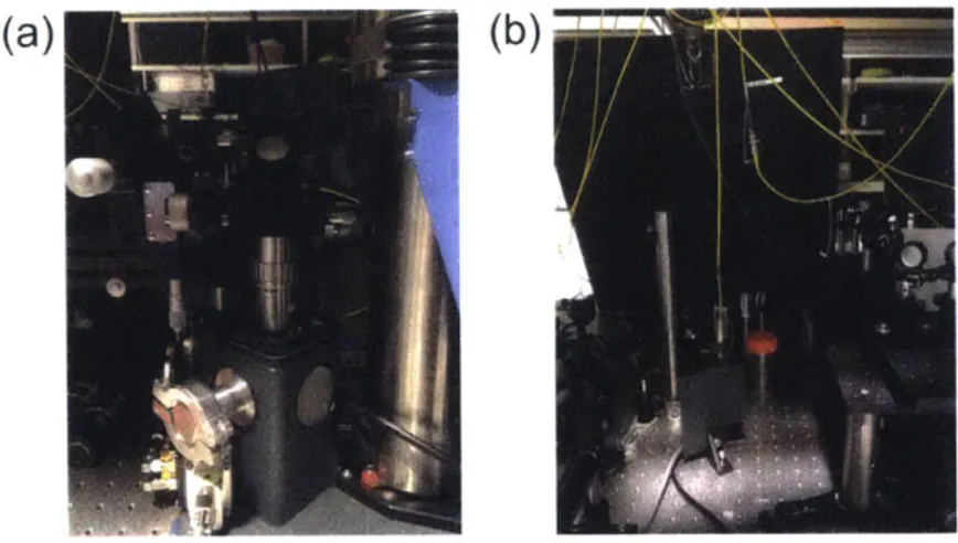
in an effective translation of the sample during imaging without actually moving the sample. The 4F is two lenses placed at a sum of the focal distance of each of the two lenses away from each other. Then, one lens is placed at a focal distance away from the galvos, the other is placed at a focal distance away from the aperture of the microscope objective. The galvos will give an angle to the laser entering the 4F. The 4F will do a correction such that the beam entering the objective will have that angle without the translation with respect to the central axis.
Object space Colector lens Detector ens Image space
P2
11 1f2 f2
Figure 2-8: 4F imaging configuration [10].
The emission and image of the quantum dots then goes through the objective, 4F, and galvos. Afterwards, it goes into either a CCD camera, out-couples into a fiber to a spectrometer, out-couples into a fiber to an APD counter, or into a free-space spectrometer. When the emission is out-coupled into a fiber to the spectrometer or APD, the fiber acts as a spatial filter to get the same effect as confocal imaging optics. On the other hand, when the emission is sent into a free-space spectrometer, an actual confocal imaging system is used. Figure 2-9 is the experimental setup used for characterizing the quantum dot chips. A portion of the microscope setup is on top of an elevated optical platform so that the objective can be suspended over the Montana closed-cycle cryostat, as shown in Figure 2-10. All the beam paths are
aligned to travel parallel with the holes in the optical table. This is necessary for the X and Y translational stages that we will discuss further: Part of the optics on top of the elevated optical table are on top of a Y translational stage that travels parallel to the beam path in order to roughly translate the optics along the Y axis with respect to the sample in the cryostat. Part of the optics on top of the Y translational stage
are on top of a X translational stage that travels parallel to the beam path in order to roughly translate the optics along the X axis with respect to the sample in the cryostat. Right before the free-space spectrometer, there is a lens that focuses the collimated beam to a pinhole, followed by another lens to collimated the beam; this
is the confocal imaging optics.
To external To external spectrometer APD by fiber by fiber
Coupler Coupler Pinhole 50/50 ~ Beamsplitter Elevated Montana closed- 7 cycle cryostat Sml
Figure 2-9: Experimental setup for quantum dot experiments.
(a)
(b)
Figure 2-10: (a) Microscope objective directly over Montana cryostat. (b) Portion of setup that transitions from the elevated optical platform to the optical table.
2.4.2
Spectroscopy Experiments
For the experiments to be described, the free space spectrometer was used for all spectrum measurements, and the external APD was used for doing the confocal
scan-ning. For the spectroscopy experiments, we first do a confocal scan zoomed out to
the largest field of view possible in order to see which bullseye has an enhanced
flu-orescence at its center. Since there should be a Purcell enhancement of about 20,
we would expect good structures to have a much brighter spot than the surrounding
unpatterned bulk QD regions. This is exactly what we see in Figure 2-ll(a), where all
the bright spots coincide with the location of the bullseyes. After we know the general
proximity of each bullseye, we can zoom in to each individual bullseye by modifying
the scan area and increasing the resolution. This is done by finely controlling the
voltage applied to each galvos mirror, which finely tunes the galvos mirror positions.
Figure 2-ll(b) is a zoomed-in confocal scan of the fluorescence of a single bullseye
circular grating. We can see clearly that there is a significantly much brighter spot
at the center of the structure.
(a)
-1 -0.6 -0.6 -0.4 -0.2 ~ ~ 0 :s; 0.2 0.4 0.6 0.6 -0.6 -0 6 -0.4 -0 2 0 0.2 0.4 0.6 0.8 1 Microns (um) x10'(b}
015 016 0.17 0.18 e 2 0.19 ~ "" 0.2 0.21 0.22 0.23 0 24 0.42 0.43 0.44 0.45 0.46 0.47 0.46 0.49 0.5 0 51 Microns(um) x 10'Figure 2-11: (a) Confocal scan of the fluorescence of an array of bullseye circular gratings.
(b) Zoomed-in confocal scan of the fluorescence of one bullseye circular grating. Note: the dimensions on the side are not the actual physical dimensions of the scan, but rather the voltage applied to each galvos mirror.
Then, we can park the galvos mirrors such that the beam spot from the objective
the flip-mount mirrors such that the collection path goes into the confocal imaging optics and into the spectrometer to take the spectrum. Figure 2-13 is an example of a bullseye circular grating spectrum while Figure 2-12 shows the spectrum of the bulk quantum dots for comparison. We see a significant resonance peak at around 935nm, which is just 5nm off from the simulated spectrum shown in Figure 2-3(f). This is reasonable considering slight fabrication imperfections. It looks like the peak width is about 5nm, as simulated. However, this is not easy to see because the spectrum has some of the bulk QD characteristics added to the resonance peak. This is probably due to the excitation beam and collection spot size being bigger than the bullseye structure. This can be fixed either by using a higher NA objective or reducing the pinhole size in the confocal imaging optics.
Figure 2-12: Spectrum of the bulk quantum dots at an unpatterned area.
/
90 1 00 0050 0 000
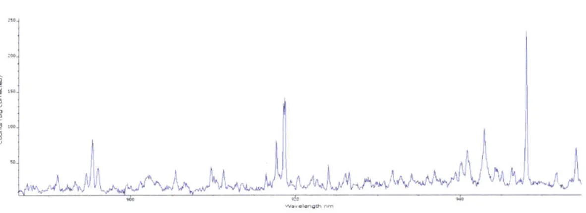
Figure 2-13: Spectrum at the center of a bullseye structure with a bright enhanced fluores-cence spot.
Figure 2-14: Spectrum at the center of a bullseye structure with a bright enhanced
fluores-cence
spot, using a higher density grating andlower
pump power.The next step for characterizing the bullseye structures would be to use a higher density grating in the spectrometer in order to get a higher resolution spectrum. Using this grating, the pump power is decreased until single exciton lines like the ones shown in Figure 2-14 can be seen. At sufficiently low pump power, we should be able to see a single exciton line that gets dramatically enhanced when the respective
QD
overlaps with a cavity both spatially and spectrally. However, that is somethingwe have not been able to observe. Usually to get a
QD
that overlaps with the cavityperfectly spatially, we would need to tune the
QD
emission wavelength by tuning thetemperature. Nonetheless, this did not seem to work, and it did not appear as if
the
QD
emission spectrum was changing when the cryostat temperature was tuned.A potential explanation for this is that perhaps the sample was not making a good thermal contact with the cryostat cold head, so it was not actually at the temperature we desired it to be. This is something to be sorted out in the near future.
Once we can determine from spectroscopy experiments that we have a
QD
that isaligned perfectly spatially and spectrally to a bullseye, then the emission can be sent to a Hanbury Brown-Twiss interferometer that uses APDs for detection to measure the photon autocorrelation statistics to check the single-photon characteristics of that
QD.
Once a goodQD
in a good bullseye structure is found, then we wouldpick-and-place the bullseye membrane onto a fiber facet and repeat the same experiments while expecting higher collection efficiency. This can also be extended to Li et al.'s previous work in which they demonstrated record-high photon collection rate from a single NV
center by using bullseye circular gratings [121. By integrating the bullseye structure with an NV in it to the facet of a high NA fiber, we can expect to get an even higher photon collection rate.
Chapter 3
Quantum Repeater using NV and
Wide-Bandgap Programmable
Nanophotonic Processor
3.1
Overview and Vision
For this portion of the thesis, I will highlight our efforts to create a quantum repeater for long-distance quantum communication and distributed quantum computing. For this, we will be using nitrogen vacancy centers in diamond as quantum memories. We also need to be able to generate entanglement between two quantum memories on-chip by entangling the photons that are entangled with each quantum memory. To do so, we would need a wide-bandgap programmable nanophotonic processor (or cir-cuit) that is capable of entangling visible wavelength photons between two quantum memories on chip via a 50:50 splitter and detection via superconducting nanowire single-photon detectors (SNSPDs) at the output arms. As we have in our arsenal the pick-and-place membrane transfer method, we can use different material systems for this method by fabricating the different components separately and transferring them to the host device with the programmable nanophotonic processor. As such, we require the host device material to be a wide bandgap semiconductor, with high
thermal conductivity and small thermo-optic coefficient so that the entire system can be placed in a cryostat and remain operational since the SNSPDs operate at cryogenic temperatures. In addition, we require the host device material to have electro-optic tuning capabilities in order to tune on-chip filters and phase shifters. Figure 3-1 is an overview of the quantum repeater hardware that we propose. The AlN dynamic photonic routing circuit is an optical mesh of cascaded tunable Mach-Zehnder inter-ferometers with phase shifters for accurately tuning the output splitting. These phase shifters are necessary since it is typically impossible to make directional couplers with exact 50:50 splitting ratios, so the phase shifters help compensate for these fabrica-tion imperfecfabrica-tions. In addifabrica-tion, the programmable nanophotonic processors can be programmed to implement any arbitrary unitary optical transformations.
Quantum Repeater Hardware
Nitrogen Vacancy in Diamond Qubits:" NV-: ion 'trapped' diamond lattice
-Electron T2 -second
* Two-qubit gates & error correction Electrical Control
Cavity Interface to Qu. Register Couplers
--Optical Control
QR1
repeater module
- Detector
QR8 AIN Dynamic Photonic Routing quantum registers
Control, Comm, Cooling
Figure 3-1: Overview of quantum repeater hardware, which uses nitrogen vacancy centers in diamond as quantum registers, AIN photonic integrated circuit for dynamic photonic routing, and SNSPDs as on-chip detectors.
3.2
Aluminum Nitride
For our host device material, we decided to use aluminum nitride since it has a large
bandgap of 6.2 eV, high thermal conductivity of KAIN= 285 W/m-K, small
thermo-optic coefficient of dnAIN/dT = 2.32 x 10-'/K, a fairly good electro-thermo-optic coefficient
of r32, r13 ~ 1 pm/V, and an added bonus of x(2) of about 4.7 pm/V. The large
bandgap means that AlN can operate in the ultraviolet, visible, and mid-infrared. Its high thermal conductivity and small thermo-optic coefficients mean that we can operate the entire device at cryogenic temperatures without the optical and physical properties of the AlN changing too much. The electro-optic coefficient is useful for tuning the optical properties of the AlN by applying an electric field across it. Finally, even though its x(2) is no match for lithium niobate's X(2) of 16 pm/V, AlN is an easier material to process and fabricate compared to lithium niobate. The X(2) allows for frequency doubling, parametric frequency conversion, sum/difference frequency generation, electro-optic modulators, optical parametric oscillators, frequency combs, and much more. Frequency conversion is especially useful for interfacing the NV quantum memories with telecom photons that are usually used as flying qubits for long distance communication.
To scalably create many of these AlN programmable nanophotonic processor de-vices sometime in the future, we would need an AlN foundry process similar to the one for silicon photonics of today, where there are multi-project runs that help distribute fabrication costs amongst a larger number of end-users. One of the long term goals, which I have started doing for this Master's Thesis, is to work with Sandia National Laboratories to develop a large-scale AlN fabrication process.
77 Massachusetts Avenue Cambridge, MA 02139 http://libraries.mit.edu/ask
DISCLAIMER NOTICE
Due to the condition of the original material, there are unavoidable
flaws in this reproduction. We have made every effort possible to
provide you with the best copy available.
Thank you.
Chapter 4
Passive Components of Aluminum
Nitride Photonic Integrated Circuit
4.1
Adiabatic Waveguide Taper
The diamond nanobeam cavity membranes with an implanted nitrogen vacancy cen-ter in the cencen-ter will be pick-and-placed onto the AlN photonic integrated circuit at a waveguide taper region that adiabatically transitions between the diamond mem-brane's waveguide mode and the AlN waveguide's mode. This design is taken exactly from a previous publication in my group by Mouradian et al. in 2014 [141, with a pertinent figure shown in Figure 4-1. The optimal device geometry was found by calculating the coupling efficiency from the fundamental TE mode of the diamond microwaveguide and the SiN waveguide while sweeping both the diamond microwaveg-uide and SiN wavegmicrowaveg-uide taper lengths. Since SiN and AlN have very similar refractive indices at 637 nm (2.01 versus 2.15, respectively), we can expect the same waveguide taper in SiN to behave closely when applied to AlN.
The paper showed that a 2 Lm gap in the SiN waveguide, a SiN waveguide taper length of 5 pLm, and a diamond microwaveguide taper length of 6 tm would result in a coupling efficiency of 41.5% coupled to each side of the SiN waveguide separated by the gap (or 83% total into the SiN waveguide).
diamond micro-waveguides SiN waveguides
w
C 0 0 0.86 0.820.78 ---. - NV to diamonddiamond to SiN
.560 600 640 680 720 760
Wavelength (nm)
Z
Figure 4-1: Adiabatic waveguide taper for coupling light efficiently from diamond nanobeam cavities to AIN waveguide. This design is taken exactly as-is from Mouradian et al.'s 2014 paper [141.
4.2
Bragg Grating Filter
(a)
Thickness = 200nm(b)
400nm 280nm 72nm(c)
Effective mode index = 1 .89868
I
i
(d)
Effective mode index =1 810855
Figure 4-2: (a) Overall design of Bragg Grating filter, which is used for filtering the 532 nm green excitation laser and allowing the 637 nm NV fluorescence to pass through. (b) Dimensions of the Bragg Grating filter, where the period is 144 nm, the original waveguide width is 400 nm, the corrugated waveguide width is 280 nm, and the thickness of the waveguide is 200 nm. (c) Electric field profile of the larger width 400 nm cross section, which has an effective mode index of 1.89868. (d) Electric field profile of the smaller width
280 nm corrugated cross section, which has an effective mode index of 1.810855.
As shown in Figure 4-2, this is the design and Lumerical MODE Solutions
simu-I
lation results of the waveguide Bragg Grating filter. Figure 4-2(a) shows the overall design and what it looks like when the Bragg Grating filter is repeated for 25 periods. Simply put, the design is a strip of waveguide with periodic sidewall corrugations, which results in a periodic modulation of the effective refractive index of the optical mode. At each corrugation boundary, part of the travelling light is reflected, where the relative phase of the reflected light is a function of the grating period and the light wavelength. As such, a Bragg Grating can be thought of as a 1D photonic crystal, so the filtering property is a result of the photonic bandgap that is formed in this structure. The repeated corrugation in the wavelength causes multiple and dis-tributed reflections, and the reflected light interferes constructively in a narrow band around the Bragg wavelength. Outside this wavelength band, the multiple reflections interfere destructively and result in the light being transmitted through the grating. Figure 4-2(b) shows the exact dimensions of the Bragg Grating filter, where the pe-riod is 144 nm, the original waveguide width is 400 nm, the corrugated waveguide width is 280 nm, and the thickness of the waveguide is 200 nm. The rough design was done by finding the neff of the region with the larger waveguide width of 400 nm and the ne.U for the smaller waveguide width of 280 nm, followed by using the Bragg condition:
o = 2neff A
A = (4.1)
2
neff
where A0 is the wavelength of the green excitation laser we want to reflect and filter, which is 532nm. nfeff is the effective refractive index of the complete Bragg Grating filter, which we take to be approximately equal to the average of the effective mode index of the wider and thinner cross sections of the filter. Finally, A is the grating period. The transmission and reflection spectra of a Bragg Grating can be calculated analytically using Coupled Mode Theory, which says that the reflection coefficient for a grating of length L is