Characterization of Novel III-V
Semiconductor Devices
by
Sue Y. Young
B.S. Electrical Engineering
Massachusetts Institute of Technology 2005
Submitted to the Department of Electrical Engineering and Computer Science in partial
fulfillment of the requirements for the degree of
Master of Engineering in Electrical Engineering and Computer Science
at the
MASSACHUSETTS INSTITUTE OF TECHNOLOGY
June 2006
HU -WNS E
OF TECHNOLOGY
AUG
1
I42006
LIBRARlgES
D 2006 Massachusetts Institute of Technology. All rights reserved.
A uthor ...
...
Sue Y Young
Department of Electrical Engineering and Computer Science
May 26, 2006
Certified by ...
.-Accepted by ...
...
slie A. Kolodziejski
uter Science
s Supervisor
...
-.iur C. Smith
Chairman, Department Committee for Graduate Students
Characterization of Novel III-V
Semiconductor Devices
by
Sue Y. Young
Submitted to the Department of Electrical Engineering
and Computer Science on May 26, 2006 in partial fulfillment
of the requirements for the degree of
Master of Engineering in Electrical Engineering and Computer Science
ABSTRACT
This thesis presents the characterization of tunnel junctions and tunnel-junction-coupled
lasers. The reverse-biased leakage current in a tunnel junction can be exploited to tunnel
electrons from the valence band of one active region to the conduction band of a second
active region. Thus, tunnel-junction-coupled lasers are highly efficient as they allow
elec-trons to stimulate the emission of photons in more than one active region. The electrical
characterization of InGaAs/GaAs tunnel junctions is presented. This thesis also gives an
overview of the electrical and optical behavior of single-stage lasers as well as two-stage
lasers coupled by InGaAs/GaAs tunnel junctions. Telecommunication applications
moti-vated the use of InAs quantum dots and InAsP quantum dashes in the active layer design
to provide near-infrared emission.
Thesis Supervisor: Leslie A. Kolodziejski
Acknowledgements
First and foremost, I would like to thank Professor Leslie Kolodziejski for having faith in me from the moment I disclosed an interest in photonics, despite my inexperience and lim-ited background. Needless to say, this year and this thesis would be impossible without her and her incredible guidance. Moreover, her commitment and dedication to her students, both as a teacher and as a supervisor, is so remarkable, and I am extremely thankful and privileged to have worked with her during my time at MIT.
This year would also not have been possible without the help of Dr. Gale Petrich. His con-stant insight and support were invaluable, and he never once hesitated to answer one of my many, many, many "quick questions," as trivial or long as they always were. I am so lucky to have collaborated with someone with such a devotion to and enthusiasm for great research.
I would especially like to give huge thanks to Dr. (forthcoming) Ryan D. Williams for
being a fantastic officemate. Not only did he develop the foundation to this project and let me shadow him in the clean room, but he always listened to my stories and enlightened me on topics ranging from wedding registries to life as a grad student and everything in between.
I'd also like to thank Jim Daley in the Nanostructures Laboratory and Leo Missaggia at MIT Lincoln Laboratory who made it possible for these devices to even be tested, and my groupmates Reggie Bryant and Alex Grine for helping me out on the weekends. I am also grateful to all the students in the CIPS community who have entertained my questions, lent me equipment, and let me stand in their way. And, of course, I can also never thank Anne Hunter enough for her answers and support over the past five years.
I must also send love and thanks to all my friends who have made my transition out of
col-lege so easy and absolutely amazing. In particular, I'd like to thank my roommates for absurd and not-so-absurd sports, cooking spices, party themes, and unconditional support. Most importantly, I'd like to thank my mom who is the best role-model, friend, mentor, and mother a daughter could ever dream of; my dad whose love, patience, and intellect I live to emulate; and my sister who is my best friend and whose advice, humor, and hugs I can't imagine life without.
THANKS!!!
Table of Contents
ABSTRACT
3
1.0 INTRODUCTION
15
2.0 TUNNEL JUNCTION DIODES 18
2.1 Background and Design Theory
18
2.1.1 What is a Tunnel Diode? 18
2.1.2 Design and Simulation 22
2.2 Research Approach 25
2.2.1 Research Objective 25
2.2.2 Fabrication Sequence 25
2.2.3 Testing Design 26
2.3 Results and Discussion 27
2.3.1 Ellipsometer Results 27 2.3.2 Fabrication Results 29 2.3.3 Electrical Results 31
3.0 QUANTUM DOT AND QUANTUM DASH
LASERS 40
3.1 Background and Design Theory 40
3.1.1 Semiconductor Lasers 403.1.2 Laser Structures 45
3.1.3 Tunnel-Junction-Coupled Lasers 46
3.1.4 Quantum Dots 47
3.1.5 Quantum Dashes 48
3.1.6 Design of Quantum Dot Lasers 48 3.1.7 Design of Quantum Dash Lasers 50 3.1.8 Laser Fabrication 51
3.2 Research Approach
52
3.2.1 Research Objective 52 3.2.2 Laser Mounting Design 53 3.2.3 Electrical Testing Design 553.3 Results and Discussion 58
3.3.1 Packaging 58 3.3.2 Quantum Dots 59 3.3.3 Quantum Dashes 61 3.3.4 Future Work 61
4.0 SUMMARY
65
5.0 REFERENCES 68
6.0 APPENDIX 70
6.1 SimWindows Simulations
70
6.1.1 Device File 70 76.2.3 15% Sample 77
List of Figures
FIGURE 1.1 FIGURE 1.2 FIGURE 2.1 FIGURE 2.2 FIGURE 2.3 FIGURE 2.4 FIGURE 2.5 FIGURE 2.6 FIGURE 2.7 FIGURE 2.8 FIGURE 2.9 FIGURE 2.10 FIGURE 2.11 FIGURE 2.12 FIGURE 2.13 FIGURE 2.14 FIGURE 2.15 FIGURE 2.16 FIGURE 2.17 FIGURE 2.18 FIGURE 2.19Attenuation and dispersion in silica core fiber [3]. ... 16
Bandgap energy and lattice constant of III-V semiconductors at room temperature [3].. 16 Band diagram and voltage-current response of a tunnel diode at equilibrium... 19 Band diagram and voltage-current response in forward bias at the point of maximum tunneling current... 19
Band diagram and voltage-current response under forward bias at the local current m inim um ... 20
Band diagram and voltage-current response under a large forward bias, inducing a therm al current... 20
Band diagram and voltage-current response under reverse-bias... 21 Structure of tunnel junction diode (not to scale), with Indium content (x) of 0%, 5%, 10% , and 15% ... 22
Band diagram of an InGaAs tunnel diode for an Indium content of 0%, 5%, 10%, and 15 % ... 2 3 Effect of a -lV reverse bias and a +1V forward bias on a tunnel diode composed of
InO.15G aO.85A s. ... 23
Simulated Zener breakdown of a GaAs tunnel diode... 24 Simulated forward tunneling characteristics of a GaAs tunnel diode... 24 Rapid thermal anneal sequence demonstrating the intermediate temperature stabilization step s... 2 6
Final structure of the tunnel junction diode... 26
Photograph of tunnel junction diode testing setup. ... 27
Variable angle spectroscopic ellipsometry testing setup. ... 28
Ellipsometry results for the MBE-grown tunnel junction diode with 5% Indium at an angle of 75 degrees... 28 VASE determined results, including the percentage of Indium (x) and the thicknesses of
the layers in the tunnel junction... 29
Nomarski micrographs of the InO.13 5GaO.8 65As tunnel junction diode after etching the co ntacts... 30
Current response of a 6.5% Indium tunnel junction sample for various contact sizes... 31 Forward tunneling behavior for 6.5% Indium for various contact sizes. Inset shows the forward tunneling behavior normalized by contact area ... 32
FIGURE 2.22 FIGURE 2.23 FIGURE 2.24 FIGURE 2.25 FIGURE 2.26 FIGURE 2.27 FIGURE 3.1 FIGURE 3.2 FIGURE 3.3 FIGURE 3.4 FIGURE 3.5 FIGURE 3.6 FIGURE 3.7 FIGURE 3.8 FIGURE 3.9 FIGURE 3.10 FIGURE 3.11 FIGURE 3.12 FIGURE 3.13 FIGURE 3.14 FIGURE 3.15 FIGURE 3.16 FIGURE 3.17
resistance for increasing Indium content... 34
Forward tunneling characteristics showing the trends in negative tunneling resistance as well as the peak and valley voltages and currents for increasing Indium content. ... 34
Normalized tunneling resistance for increasing Indium concentration... 36
Fitting the first term of Equation 2.1 to the experimental data by varying the peak voltage and peak current density to minimize the squared error... 37
The fitted values of the peak voltage and peak current... 37
Effect of annealing on reverse-biased tunneling resistance... 38
Temperature effect on reverse-biased tunneling resistance... 39
Three types of electron-photon interaction... 40
Fabry-Perot cavity and m odes ... 41
Optical gain and loss versus drive current density. ... 42
Relationship between the optical power generated for a given current injection... 43
The effect of temperature on optical power output and threshold current. ... 45
Tunnel-junction-coupled laser depicting how electron tunneling can stimulate emission in tw o lasers... 46
Density of states diagram for bulk, quantum well, and quantum dot structures... 47
Device structure of the quantum dot lasers. ... 49
Atomic force microscopy of gas source molecular beam epitaxially-grown InAs quantum d o ts [6]... 5 0 Device structure of quantum dash laser... 50
Scanning electron micrograph (SEM) of the InAs0 9P0.1 quantum dashes grown using M B E . ... 5 1 Nomarski micrograph of the quantum dash laser (II). ... 52
D im ensions of copper m ounts ... 53
Structure of metals used to solder the GaAs or InP device to a copper mount... 54
Structure of metals used to solder the GaAs and InP devices to a CuW mount... 55
Diagram of continuous operation testing using an InGaAs photodetector...55
Wavelength detection range of an PbS detector [20] ... 56
FIGURE 3.18 FIGURE 3.19 FIGURE 3.20 FIGURE 3.21 FIGURE 3.22 FIGURE 3.23 FIGURE 3.24 FIGURE 3.25
Diagram of continuous or pulsed operation testing using an PbS photodetector... 56
Schem atic of PbS detector circuit... 57
Room temperature photoluminesence of quantum dot laser epilayer [20]... 58
Voltage characteristics of a single stage and two stage laser... 59
Output power for a single and two-stage laser. ... 60
Heating effects on output behavior due to slow continuous operation. ... 61
Structure of a stripe laser, demonstrating lateral current spreading. ... 62
Structure of a ridge laser with adequate lateral carrier confinement...62
List of Tables
TABLE 1. Typical Parameters of Tunnel Diodes... 22 TABLE 2. Final diameters of the contacts following the fabrication sequence... 30
TABLE 3. Median experimental values of peak current, normalized peak current, valley current,
normalized valley current, peak voltage, valley voltage, current ratio, and normalized minimum resistance for different percentages of Indium... 35
TABLE 4. Impedance values for the PbS detector circuit. ... 57
TABLE 5. Lasing parameters of a 26.1 x 930 gm single-stage laser and a 26.7 x 1002 gm two-stage
laser...6 0
INTRODUCTION
1.0 INTRODUCTION
Semiconductor lasers play an essential role in a variety of fields, including medicine, atmospheric testing, manufacturing, and the entertainment industry. Additionally, highly-efficient laser diodes have revolutionized the telecommunication industry. Coupled with silica fibers, these devices are implemented in large-scale optical networks around the world. Compared to electrical-based telephony systems, photonic technology offers many benefits: higher bandwidth and thus higher information transmission rates; less interfer-ence from other electrical equipment and therefore lower crosstalk; good information retrieval; and parallel access of information. While metropolitan areas are connected together via optical networks, direct user connectivity is not yet as widely implemented due to higher costs, creating a bandwidth bottleneck for the user.
Fiber to the Home (FTTH) is one example of a point-to-multipoint network and telecom-munication system that could potentially provide telephone, broadband internet and televi-sion to homes and businesses in one bundle. FTTH has already been implemented in countries in North America, Europe, the Middle East, and Asia. Japan leads the effort with 4.63 million connections as of March, 2006 [1]. The demand in the United States is quickly increasing as well; the Telecommunications Industry Association reported in April
2006 that 936 communities in 47 states offer FTTH broadband solutions, which includes a 107 percent increase in connections as of October 2005. Though costs still need to fall,
global acceptance and demand are inevitably increasing [2].
One form of FTTH is based on a passive optical network (PON) which uses passive split-ters to distribute fibers to individuals, eliminating the need for neighborhood electrical equipment. The PON uses wave-division multiplexing (WDM) such that three streams of data are sent on a single fiber: telephone, internet, and video services are received at 1490 nm and 1550 nm, and data is transmitted at 1310 nm.
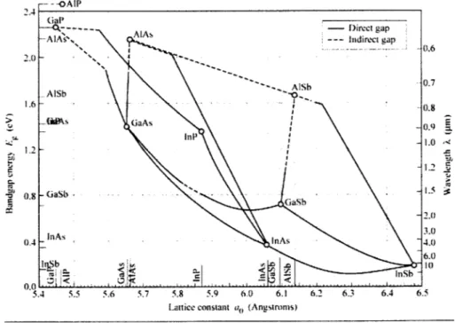
High-efficiency lasers at these wavelengths are desired as they offer minimal dispersion in optical fibers. As shown in Figure 1.1, attenuation is minimized at 1550 nm, and disper-sion is minimized at 1300 nm. However, Figure 1.2 demonstrates that no binary material system has the corresponding bandgap energy to emit at these wavelengths.
FIGURE 1.1 Attenuation and dispersion in silica core fiber [3]. 100 I.. I I 10 0.1 0.01 0.6 0.8 1.0 1.2 Waveleneth ) (pil) 1.4 1.6 1.8
FIGURE 1.2 Bandgap energy and lattice
2- --OAIP C. ~jJ C 2.0 1.6 1.2 0.8 0.4 5.4 5.5
constant of III-V semiconductors at room temperature [3].
5.6 5.7 5.8 5.9 6.0 6.1 6.2 6.3 6.4 6.5
Lattice constant a0 (Angstroms)
Characterization of Novel III-V Semiconductor Devices
I I = Silica libers - -- Measurement rO absorpton - - - - -Theoretical limits RaN leih '-m scatterino - /= -Infrared absorption Glap
A-- - -- Direct gap
-A As~ AlAs --- Indirect gap
- . x-, -AlSb - AISb GaAs II Asb G As Gans <~ b -ll E-i=. 0.6 0.7 0.8 0.9 1.0 1.2 1.5 2.0 3.0 4.0 6.0 10 I I
i
16INTRODUCTION
One of the technologies developed to provide 1300 nm emission involves the use of InAs quantum dots on GaAs wafers in which the Stranski-Krastanov growth of InAs on GaAs is exploited. This technology has also been expanded to other wavelengths. Specifically, InAs-based quantum dashes, which are elongated quantum dots, on InP-based material alter the bandgap such that these lasers will be able to emit wavelengths between 1500 nm to 1800 nm.
Nonetheless, a limiting factor that all semiconductor lasers in these applications share is that one electron can release at most one photon. High-efficiency lasers are often desired as they consequently offer higher output powers and lower threshold currents.
Circumnavigating the injection current efficiency limit is possible by incorporating a tun-nel junction. Fabricating lasers in series via a tuntun-nel junction diode can dramatically increase the lasing efficiency.
Therefore, cascading lasers together with tunnel junctions allow multiple photon emission for every electron, while the use of quantum dots and dashes expand the wavelength emis-sion range in the near-infrared region. Chapter 2 will investigate the behavior of InGaAs tunnel junction diodes for different percentages of Indium. A low resistance tunnel junc-tion would increase the tunneling of electrons and thus the quantum efficiency of a device incorporating the tunnel junction. Chapter 3 will characterize single stage GaAs-based quantum dot lasers, tunnel-junction-coupled quantum dot GaAs-based lasers incorporat-ing Indium tunnel junctions, and InP-based quantum dash lasers. Chapter 4 summarizes the overall results and comments on future directions.
2.0 TUNNEL JUNCTION DIODES
As optical transmitters, semiconductor lasers often require high output powers with low threshold currents. However, most lasers are inherently limited to 100% injection current efficiency, where one photon is emitted for every electron. Fortunately, cascade lasers overcome the maximum quantum efficiency of a single laser; in a cascade laser, individual lasers are placed in series with each other so that a single electron can flow through and stimulate emission in each device. The differential efficiency, given by the amount of light emitted over current, increases by the number of stacked stages.
Electrically connecting individual laser diodes in series suffers from many parasitic impedances and is hard to couple into a single fiber. As a result, the overall performance of the system is significantly reduced. Connecting the lasers in series during the epitaxial growth process provides an excellent alternative and is accomplished with a Tunnel Junc-tion. [4]
A tunnel junction works by simply exploiting the reverse-biased leakage current of a
highly-reversed biased heavily-doped diode. Coupled between the two lasers, the tunnel junction diode allows an electron to tunnel from the valence band of the first laser, after stimulating emission, to the conduction band of the second laser.
This chapter introduces and characterizes InGaAs tunnel diodes. The incorporation of Indium can lower the bandgap and effectively improve the tunneling performance of the device.
2.1 Background and Design Theory
2.1.1 What is a Tunnel Diode?
The tunnel diode is a typical p-n junction with the exception that both the p-side and n-side of the device are degenerately-doped. As a result, the Fermi-levels are located within the conduction band for the n-type material and within the valence band for the p-type mate-rial.
Figure 2.1 shows the band diagram and electrical characteristics of a highly degenerately-doped diode at equilibrium with no net current flow. When a forward bias is applied, a net current from the n- to the p-side occurs. The quasi-Fermi level of the n-doped side increases with respect to the doped side and electrons consequently tunnel to the p-doped side of the device, increasing the current.
Characterization of Novel Ill-V Semiconductor Devices 18
TUNNEL JUNCTION DIODES
FIGURE 2.1 Band diagram and voltage-current response of a tunnel diode at equilibrium.
p type
EC
E F "" " " ."" ... "" "" 'E...
...
.
n type
IV
EV
Eventually, the tunnel current reaches a local peak when the maximum number of occu-pied states in the conduction band on the n-side is aligned with the maximum number of unoccupied states in the valence band on the p-side. This is shown in Figure 2.2. Increas-ing the forward bias further brIncreas-ings the n-side conduction band and the p-side valence band gradually out of alignment and reduces the current. The point of local minimum is shown in Figure 2.3 and depicts the point at which the occupied and unoccupied states are no longer aligned. Ideally, the current should go to zero, as tunneling across the junction is no longer possible. However, an excess current exists; electrons tunnel via energy levels within the bandgap due to the spread in the dopant impurity ionization energy and indirect tunneling.
Band diagram and voltage-current response in forward current.
p type
EC
EF ... " '"n type
bias at the point of maximum tunneling
EV
Characterization of Novel III-V Semiconductor Devices FIGURE 2.2
Band diagram and voltage-current response under forward bias at the local current minimum.
p type
EC
E . . . . . .. ...EFntype
n type
V
Further increasing the forward bias, the tunnel junction device begins to behave similar to a regular p-n diode. Electrons and holes are injected over their respective barriers, result-ing in the diffusion of minority carriers typically seen in a normal p-n junction. This cur-rent is demonstrated in Figure 2.4.
Band diagram and voltage-current response under a large forward bias, inducing a thermal current.
p type
Ec
EF...
E.
n type
I
V
Characterization of Novel III-V Semiconductor Devices FIGURE 2.3 FIGURE 2.4 r- 1 :2 I I 20
TUNNEL JUNCTION DIODES
Band diagram and voltage-current response under reverse-bias.
p type
EF
---n type EV
A
Figure 2.5 shows the device in reverse bias. Raising the p-side quasi-Fermi level above the n-side quasi-Fermi level promotes the tunneling of electrons from the occupied states in the valence band on the p-side to the empty states in the conduction band on the n-side. Increasing the negative bias further increases the negative tunneling current. This phe-nomenon of Zener tunneling, where electrons can move from the valence band of one device to the conduction band of the next, allows semiconductor lasers to be connected epitaxially in series.
Given an applied voltage, the current in a tunnel diode is given by
(EQ 2.1)
I = Ip(- - exp(1
-)
+ Io- exp(1 - + Iexcesswhere the first term models the tunneling current, where Ip and Vp are the peak current
and peak voltage, respectively. The second term explains the behavior seen diode, modeling the current due to the diffusion and drift of minority carriers. ing resistance can be obtained from the first part of Equation 2.1 and is given 2.2. R = 1 -IVexp 1 in a simple The tunnel-in Equation (EQ 2.2)
When the tunnel diode is forward biased, the point at which the negative slope is maxi-mum gives the minimaxi-mum negative resistance. This value can be approximated as follows:
(EQ 2.3)
2Vp
'P
This negative resistance is often exploited for switching, amplification, and oscillation purposes, and therefore implemented in high speed switching circuits and microwave amplifiers and oscillators. Typical values of the peak-to-valley current ratio (Ip/IV), the
Characterization of Novel III-V Semiconductor Devices FIGURE 2.5
.... ... ...
j
peak voltage (Vp), and the valley voltage (VV) of Ge, Si, and GaAs tunnel diodes are listed in Table 1. [5]
Typical Parameters of Tunnel Diodes.
Semiconductor IP'I VP (9 VV
Ge 8 0.055 0.35
Si 3.5 0.065 0.42
GaAs 15 0.15 0.5
2.1.2 Design and Simulation
The incorporation of Indium in a GaAs tunnel diode has the potential to further increase the tunneling current in the device by decreasing the bandgap. Figure 2.6 depicts a simple degenerately-doped p-n junction diode.
Structure of tunnel junction diode (not to scale), with Indium content (x) of 0%, 5%, 10%, and
15%.
InxGal-,As:p++ 25 nm
In-Ga.As:n++ 25 nm
Degenerate doping is required to move the quasi-Fermi levels of the diodes into the con-duction and valence bands. The device was grown using a Gas-Source Molecular Beam Epitaxy (GSMBE) system. The epilayer structure was grown at a rate of approximately
0.5 gm/hour and at a substrate temperature of 480'C. Hall measurements of heavily
n-and p-type doped GaAs, using Si n-and Be as dopants, confirmed high doping concentra-tions of approximately 1 x 1019 cm-3. The desired Indium content for the tunnel juncconcentra-tions were 0%, 5%, 10%, and 15%. [6]
Figure 2.7, shows the band diagrams of the InGaAs tunnel diode at equilibrium with an Indium content of 0%, 5%, 10%, and 15%. The device is sandwiched between doped GaAs. As the Indium content is increased, the decrease in bandgap is clearly demon-strated. The jumps at the junction interfaces are attributed to the slight inconsistencies between the GaAs material model and the InGaAs material model. Material parameter files and device files can be found in Appendix 6.1.
Characterization of Novel III-V Semiconductor Devices TABLE 1.
FIGURE 2.6
TUNNEL JUNCTION DIODES
Band diagram of an InGaAs tunnel diode for an Indium content of 0%, 5%, 10%, and 15%.
04 0.45 0.5 0.55 0.6 5% Indium 5--7 -8--0] 04 0.455 0.55 0.6 0% Indium -6 -81 404 0.45 0.5 0.55 0 .6 10% Indium
-5--Ec (eV) - Efn (eV) -Ev (eV) - Efp (eV)
4 0.45 0.5 0.55 0.6
15% Indium
Figure 2.8 shows the effect of a forward and reverse bias on the band structure. The diffu-sion of minority carriers occur with a positive applied bias. With a negative applied bias, the quasi-Fermi levels are now aligned such that tunneling is encouraged.
FIGURE 2.8 Effect of a -IV reverse bias and a +1V forward bias on a tunnel diode composed of Ino 15Gao.85As.
4 045 0.55 Q6
+1 V applied bias
- Ec (eV) - Efn (eV) -Ev (eV) - Efp (eV)
4 0.45 0.5 0.55 0.6
-1 V applied bias
The effect of the reduced bandgap can be directly demonstrated by plotting the tunneling current response of the tunnel diode given an applied bias. Figure 2.9 and 2.10 simulates the current density response for a given applied voltage. Figure 2.9 shows the Voltage-Current behavior of GaAs tunnel diode, clearly demonstrating a Zener tunneling current.
A closer view of the origin in Figure 2.10 depicts the forward tunneling current.
Characterization of Novel III-V Semiconductor Devices FIGURE 2.7 -6 .5 -1 6 .7 -8-.-4 -8 23
FIGURE 2.9 Simulated Zener breakdown of a GaAs tunnel diode. Applied Voltage (V) 0.6 -0.4 -0.2 0.2 0.4 0 6 -1000 -5000--9000
FIGURE 2.10 Simulated forward tunneling characteristics of a GaAs tunnel diode.
IE 3
-01 0.1 0.3 0.5
Applied Voltage (V)
The first term in Equation 2.1 is used to plot the tunneling characteristics in both figures.
Vp can be calculated from
Characterization of Novel III-V Semiconductor Devices
TUNNEL JUNCTION DIODES
y = v + 3 (EQ 2.4)
where $, is the degeneracy on the n side and is given by kT F(ND\ (ND
On q [ LMcI in N+0.35. - Nc (EQ 2.5)
where ND is the donor concentration and Nc is the effective density of states at the con-duction band edge. Similarly, $p is the degeneracy on the p-side and can be calculated by equation 2.5, where ND and Nc are respectively replaced with NA, the acceptor concentra-tion, and NV, the effective density of states at the valence band edge. For GaAs with a n-and p-type doping of 1 x 1019 cm-3, the peak voltage for a 0% Indium tunnel diode is 0.095V An experimental value of 4.2 A/cm2 is used as the peak current density in Figure
2.9 and 2.10, as previously determined for a GaAs tunnel diode in [7]. 2.2 Research Approach
2.2.1 Research Objective
Our goal is to electrically characterize the tunneling behavior of the InGaAs/GaAs struc-tures. The ideal performance of the devices would not only demonstrate tunneling behav-ior but also demonstrate a decrease in resistance as the concentration of Indium is increased in the tunnel junction.
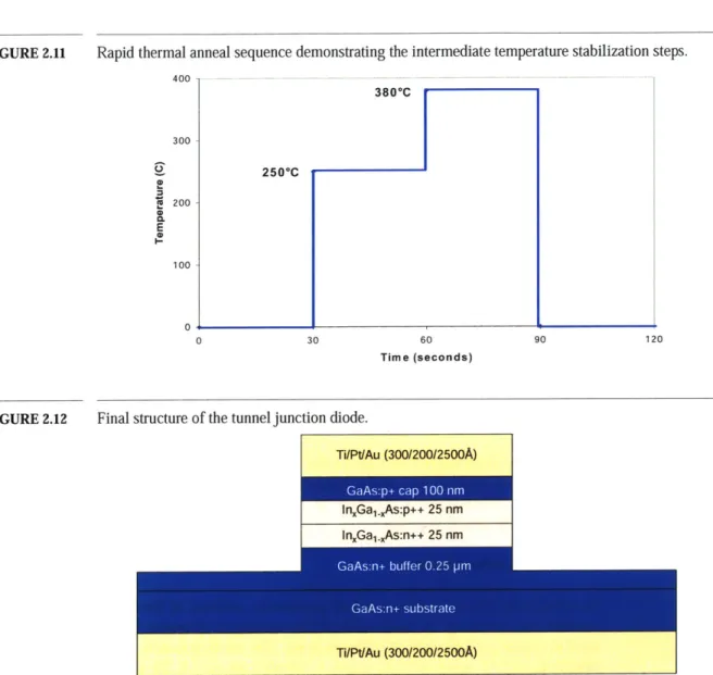
2.2.2 Fabrication Sequence
To effectively test the wafer structure previously outlined in Section 2.1.2, appropriate contacts are necessary. A mask with circles varying in diameter from 17.5 to 90 pm is used to create contact pads of different sizes. The metal contacts consisting of Ti/Pt/Au (300/200/2500A) were defined using a lift-off process. A 30 second wet etch using NH4:H 202:DI (10:5:240) isolates the individual tunnel junction devices from each other.
The wet etch etches through the upper GaAs layer and through the InGaAs layers to create well defined tunnel junctions. Ti/Pt/Au can form an ohmic contact to both n-type and p-type GaAs, so a back-side metal contact consisting of Ti/Pt/Au of the same thickness as the top contact is deposited, followed by a rapid thermal anneal (RTA) for 30 seconds at
380*C. The RTA consists of ramping steps and intermediate temperature stabilization and
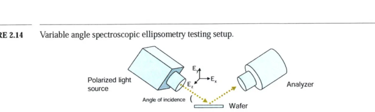
is modeled in Figure 2.11. The final device structure is shown in Figure 2.12.
Rapid thermal anneal sequence demonstrating the intermediate temperature stabilization steps. 400 -300 200 - 0-3800C 2500C 4 0 30 60 Time (seconds) 90
FIGURE 2.12 Final structure of the tunnel junction diode.
Ti/Pt/Au (300/200/2500A)
GaAs:p+ cap 100 nm~
InxGa1.-As:p++ 25 nm
In.Ga1.-As:n++ 25 nm
Ti/Pt/Au (300/200/2500A)
Photolithography is performed in the Microsystems Technology Laboratory with the help of Ryan D. Williams. All of the subsequent fabrication steps are performed in the Nano-structures Laboratory with the assistance of Ryan D. Williams. Metallization is carried out
by James Daley. 2.2.3 Testing Design
To characterize the InGaAs/GaAs tunnel junctions, voltage-current performance of the device is required. A semiconductor parameter analyzer is used to measure the output cur-rent for a given applied bias. Figure 2.13 shows a photograph of the testing apparatus.
Characterization of Novel III-V Semiconductor Devices FIGURE 2.11
120
TUNNEL JUNCTION DIODES
FIGURE 2.13 Photograph of tunnel junction diode testing setup.
A voltage sweep from -500 mV to +500 mV is applied to the various sized contacts. Thus,
the resistance for different concentrations of Indium and for different contact sizes can be calculated. The resistance should decrease for increasing pad size and decrease for increasing Indium concentrations. Forward tunneling parameters, including peak and val-ley voltages and currents, can also be obtained from the data. The effect of the final RTA step in the fabrication sequence and the effect of changes in temperature will also be ana-lyzed.
2.3 Results and Discussion
2.3.1 Ellipsometer Results
Various tunnel junctions were designed and grown to have an Indium content of 0%, 5%
10%, and 15%. Before device fabrication, the exact alloy percentage is first assessed using
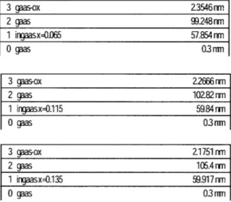
variable angle spectroscopic ellipsometry (VASE). As shown in Figure 2.14, the ellipsom-eter shines polarized light onto the sample and measures the change in polarization caused
by the structure's index of refraction to determine the thickness and composition of each
layer in the structure. Ellipsometer measurements were taken of the MBE-grown wafers with 5%, 10%, and 15% Indium at three angles of incidence: 65, 70, and 75 degrees. The analyzer was moved to the same angle as the light source.
FIGURE 2.14 Variable angle spectroscopic ellipsometry testing setup.
Polarized light E E Analyzer
source it - Ay
Angle of incidence
Wafer
At each angle, the change in amplitude, tan(W), and phase, cos(A), of the incident light were measured and fitted. Figure 2.15 depicts the experimental results as well as the model fit for the structure with a designed 5% Indium tunnel junction at a measured angle of 75 degrees, showing a very close model fit to the ellipsometer data. Appendix 6.2 includes the results for all tunnel junction samples at all three angles. The VASE model that was used to fit the data is based on the design structure as outlined in Figure 2.6 as well as an additional top layer of GaAs oxide resulting from the wafer's exposure to air. The curve fitting program uses P(X, 0) and A(X, 0) to determine the thickness and compo-sition of each layer of the dielectric stack.
FIGURE 2.15 Ellipsometry results for the MBE-grown tunnel junction diode with 5% Indium at an angle of 75 degrees.
Generated and Experimental
25 140 20- - Mod Fit - 120 --- -Exp '-E75* -- Moded Fit . > S15 15 - ' '- -- - -Exp NrzFA-E 75* = - 100 8 10 CDCD 5-016 2000 3000 4000 5000 6000 7000 8000 VMewngth (A)
For each sample wafer,
'(R,
0) and A(R, 0) were measured and fitted for angles ofinci-dence of 65, 70, and 75 degrees. The three sets of data were used to determine the GaAs thickness, the InGaAs composition and thickness, and the native GaAs oxide thickness for each wafer. Figure 2.16 shows the results determined by the ellipsometer data.
Characterization of Novel III-V Semiconductor Devices 28
TUNNEL JUNCTION DIODES
FIGURE 2.16 VASE determined results, including the percentage of Indium (x) and the thicknesses of the layers
in the tunnel junction.
3 gaas-ox 2.3546 nm 2 gaas 99.248 nm 1 ingaasx=0.065 57.854 nm 0 gaas 0.3 rim 3 gaas-ox 2.2666
nm
2 gaas 102.82 nm 1 ingaasx=0.115 59.84 m 0 gaas 03 rim 3 gaas-2 gaas 1 irigaa ox 2.1751rm 105.4 rrn sx=0.135 59.917 nm 0 gaas 03mnThe GaAs capping layer is within 5% of its designed thickness, and the tunnel junction layers are all within 20% of their designed thicknesses. The native oxide layer is small and can be removed with an initial oxide etch. Indium contents were found to be 6.5%, 11.5%, and 13.5%. These Indium compositions will be used in the analysis of the InGaAs tunnel diodes.
2.3.2 Fabrication Results
The following fabrication sequence, as outlined in Section 2.2.2 was performed on the tunnel junction diodes with 0%, 6.5%, and 11.5% Indium:
" Photolithography using image reversal resist
" Deposition of Ti/Pt/Au (300/200/2500A) " Metal lift-off
* 30 second NH4:H20 2:DI (10:5:240) etch
" Back-side deposition of Ti/Pt/Au (300/200/2500A) " RTA for 30 seconds at 380*C
The Ino.135Gao.86 5As tunnel junction diode followed the same fabrication sequence but instead underwent a 60 second NH4:H 202:DI (10:5:240) wet etch. The 30 second etch etched 225 nm while the 60 second etch etched 445 nm. Figure 2.17 shows this sample after the etch. Etching of the 0%, 6.5%, and 11.5% diodes displayed similar results.
TUNNEL JUNCTION DIODES
Nomarski micrographs of the Inn .,Gan zrAs tunnel junction diode after etching the contacts.
The size of the circle contacts were measured using a Nomarski microscope. The final diameters are listed in Table 2.
Final diameters of the contacts following the fabrication sequence. Desired diameter Actual diameter
(Am) (jim) 90 88.74 70 66.56 60 57.42 50 48.29 40 39.15 35 33.93 30 28.71 25 23.49 20 20.88 17.5 18.27
Thus, the fabrication of the tunneljunction diodes was successful, giving near perfect con-tact diameters with clean etches.
Characterization of Novel III-V Semiconductor Devices FIGURE 2.17
TABLE 2.
TUNNEL JUNCTION DIODES
2.3.3 Electrical Results Results by Contact Size
The testing setup as described in Section 2.2.3 was used to measure the current response of the tunnel junction diodes for a given applied voltage. A voltage sweep from -500 mV to
+500 mV (10 mV steps) was applied to the contacts of diameters varying from 90 gm
down to 35 gm. Measurements of the current response from the smaller contacts were dif-ficult to obtain due to the poor contact between the wafer and the current probe. Figure
2.18 shows the voltage-current characteristics for the 6.5% Indium tunnel junction diode.
As demonstrated, multiple measurements were taken, and trend lines demonstrate general consistency between the measurements. A decrease in resistance for increasing contact size is clearly demonstrated. The results of multiple measurements for the 0%, 11.5%, and
13.5% Indium tunnel junctions showed an identical trend in tunneling behavior: an
increase in contact size decreased the tunneling resistance. More importantly, all of the results demonstrate the current-voltage response of a tunnel diode as discussed in Section
2.1.1.
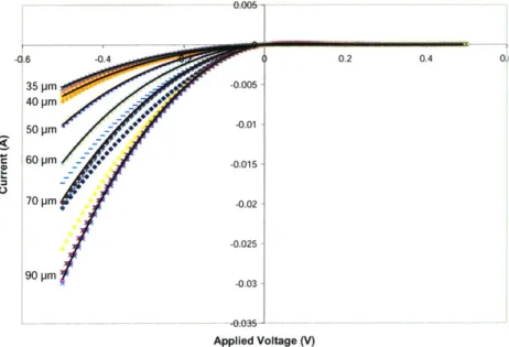
FIGURE 2.18 Current response of a 6.5% Indium tunnel junction sample for various contact sizes.
-d.6 -0.4 0.2 0.4 0.6 35 pm -0.005 40 pm -0.02 -0.025 90 pm -0.03 -0.025-Applied Voltage (V)
A closer look at the forward tunneling characteristics for the 6.5% Indium tunnel junction
device is shown in Figure 2.19. The peak and valley behavior of a tunnel diode, as previ-ously discussed in Section 2.1.1, is demonstrated. Also, the inset in Figure 2.19 shows the forward tunneling behavior normalized for area; the overlap of the data indicates consis-tency across the wafer. Again, data for the 0%, 11.5%, and 13.5% Indium tunnel
junctions
gave very similar results. Therefore, further discussion on the electrical characterization of the tunnel diodes will focus on the current density behavior unless otherwise noted.FIGURE 2.19 Forward tunneling behavior for 6.5% Indium for various contact sizes. Inset shows the forward tunneling behavior normalized by contact area.
0.00025 Nl 4-E 90pm 0.0002 2- 0.00015-70 pm.2 0.4 0.6 Applied Voltage (V) 0.0001 -60 pm 50 pm 0.00005 -35pm 0 0 0.1 0.2 0.3 0.4 0.5 0.6 Applied Voltage (V)
Indium Effects on Tunneling
For all of the devices, over 250 measurements were taken. Compilation of the results at each Indium content was done by calculating the medium current density response for each device. Figure 2.20 plots the response of current density to the applied voltage for tunnel junctions with 0%, 6.5%, 11.5%, and 13.5% Indium.
Characterization of Novel III-V Semiconductor Devices 32
TUNNEL JUNCTION DIODES
FIGURE 2.20 Reverse and forward bias current response, normalized by contact size, to an applied voltage. &.00-3.00 N 0 -0.1 'ft C 0 0 C 0 C.) -3 -. 00 9.00 200 0.1 0.2 0.3 0.4 0.5 046 Voltage (V)
Tunnelling behavior, as previously predicted theoretically, is demonstrated under reverse and forward bias. Moreover, under forward bias, the tunneling current first peaks but is then followed by a brief range of negative resistance until the thermal current begins to dominate with the forward injection of minority carriers.
Figure 2.21 shows the complete reverse-biased behavior. The tunneling resistance decreases as the Indium percentage increases; more electrons tunnel through the junction at a given applied bias, as expected for a smaller bandgap. Significantly, when imple-mented in a tunnel-junction-coupled laser, a smaller tunneling resistance would yield a more efficient laser.
Characterization of Novel III-V Semiconductor Devices
-0% -6.5% -11.5% -13.5%1
FIGURE 2.21 A magnified view of the reverse bias increasing Indium content.
current response, demonstrating a decrease in resistance for
-0. 050 -0.040 -0.030 -0.020 -0.010 0.( -3 -6 Decrease in Resistance -9 -0% -6.5% -11.5% -13.5% 00 Voltage (V)
Figure 2.22 confirms the tunneling behavior in the forward-biased region. The figure also demonstrates the trends of the device parameters, which are listed in Table 3. The peak voltage increases, though slightly, while the valley voltage decreases.
Forward tunneling characteristics showing the trends in negative tunneling resistance as well as the peak and valley voltages and currents for increasing Indium content.
0 Increas -0% -6.5% -11.50 inip Decrease in Negative Resistance Increase in VDp Increase in J v Decrease in Vv 0.1 0.2 0.3 Voltage (V) 0.4 0.5 -13.5% 0.6 E FIGURE 2.22 5 4 -3 -1 -0
Characterization of Novel III-V Semiconductor Devices 34
TUNNEL JUNCTION DIODES
TABLE 3. Median experimental values of peak current, normalized peak current, valley current, normalized valley current, peak voltage, valley voltage, current ratio, and normalized minimum resistance for different percentages of Indium.
Percentage Jv NormalizedR
of Indium Ip (A) Jp (A/cm2) Iv (A) (A/cm2) Vp () Vv M Ip/Iv (Q cm2)
0.00% 9.29E-05 2.26 4.86E-06 0.12 0.07 0.37 19.2 1.19
6.45% 1.32E-04 3.43 7.86E-06 0.20 0.07 0.37 16.7 0.69
11.50% 1.62E-04 3.68 1.15E-05 0.27 0.07 0.36 13.6 0.51
13.50% 2.90E-04 4.56 2.83E-05 0.44 0.08 0.36 10.0 0.34
From Table 3, the difference between the peak and valley voltage is 0.3 V for 0% Indium, which is very close to the value of 0.35 V listed in Table 1 as a typical device parameter of a GaAs tunnel diode. Table 1 also listed a peak-to-valley ratio for GaAs of 15, close to the experimentally determined value.
Also notable is the rise in the valley current as the percentage of Indium is increased. One possible explanation is an increase in excess current by means of electrons tunneling through the forbidden bandgap. The incorporation of Indium might have increased the number of indirect states. Also likely is that the net flow of minority carriers occurs at a lower voltage, lifting the value of valley current. This is expected as increasing the per-centage of Indium decreases the bandgap and the effective voltage at which the thermal current begins to dominate.
Additionally, the increase in slope as the quantity of Indium is increased indicates a decrease in resistance. The minimum negative resistance, as calculated from Equation 2.3, are included in Table 3 and plotted in Figure 2.23. A clear linear inverse relationship is demonstrated between Indium content and tunneling resistance.
FIGURE 2.23 Normalized tunneling resistance for increasing Indium concentration. 1.2 E E -Rmin = -6.0193x + 1.1556 0 0 4) 0 0.2 0% 5% 10% 15% % Indium Parameter Modefing
In addition to simply extracting the tunneling parameters, the tunneling parameters were determined by fitting the first term of Equation 2.1 to the experimental data close to the point of zero bias, from -70 mV to + 70 mV, by varying the peak current and voltage val-ues. The fitting results are shown in Figure 2.24 and indicate a very close fit to the experi-mental data. The values for peak voltage and peak current were determined by minimizing the squared error between the two plots. The extracted parameter values are plotted in Fig-ure 2.25. As the model for tunneling current is primarily dependent on these two parame-ters, as suggested by Equation 2. 1, an increase in both of these values would increase the tunneling current. Both of these trends are clearly demonstrated.
Characterization of Novel III-V Semiconductor Devices 36
TUNNEL JUNCTION DIODES
Fitting the first term of Equation 2.1 to the experimental data by varying the peak voltage and peak current density to minimize the squared error.
0% Indium 0 a U E 004 00 0-000 -0.04 -1 -- Experimental Data .20 - Theoretical Fit _ Voltage (V) 10% Indium 0.04 008 .008 E .201 Voltage (V)
The fitted values of the peak voltage and peak current.
0% - Jp -- Linear (Jp) JP = 16.021x + 2.5767 Vp = 0.0995x + 0.0874 5% 10% % Indium
Characterization of Novel III-V Semiconductor Devices FIGURE 2.24 5% Indium 00 Voltage (V) 15% Indium FIGURE 2.25 -0.04 Vt -20--Voltage (V) 6-4 U) 2 0 0 0.115 -0.105 -0.095 0 (U IL -i 0.085 15% P_ -0.04 ,15
5-..O
-0.04 5 -A5 _0 0.04 0o 37Effects of Annealing
Electrical characterization of the 13.5% Indium tunnel diode was performed before and after the final annealing step. All tests were preformed on a 90 gm contact, and Figure
2.26 shows the un-normalized result: annealing the device significantly decreases the
resistance of the tunnel diode. Thus, the anneal is effective in alloying the metal-semicon-ductor interface.
FIGURE 2.26 Effect of annealing on reverse-biased tunneling resistance.
-0.5 -0.4 -0.3 -0.2 -0.1 0
- 0.0E-i00
Pre-anneal data
Decrease in Resistance - .0E04
-2.OE-04 -30E-04 -4.OE-04 Post-anneal data --- -- -5.OE-04 Voltage (V) Temperature Effects
On a GaAs tunnel diode (with 0% Indium), measurements were taken at room temperature on 90 gm contacts. Measurements on the same contacts were then repeated after cooling the wafer 6C colder with Falcon Dust-Off, a Freon source. Figure 2.27 demonstrates the effect of a change in temperature on the tunneling behavior of a device. Reducing the free carrier concentration by decreasing the temperature decreases the amount of tunneled cur-rent for a given applied bias. Thus, the resistance is increased.
Characterization of Novel III-V Semiconductor Devices 38
TUNNEL JUNCTION DIODES
FIGURE 2.27 Temperature effect on reverse-biased tunneling resistance. Decreases in Temperature
Increases the Tunneling Resistance .6 -0.4 -0.2 ) 0.2 0.4 06 -0.01 r cooled -0.02 - -0.03-room temperature Applied Voltage (V)
QUANTUM DOT AND QUANTUM DASH LASERS
Background and Design Theory
3.1.1 Semiconductor Lasers
There are three main types of interactions between electrons and photons in a material: spontaneous emission, stimulated absorption, and stimulated emission. All of which are depicted in Figure 3.1.
Three types of electron-photon interaction.
Spontaneous Emission
E2
|V[\||/A hv
E 0
Stimulated Absorption Stimulated Emission
E2 0
hvN \f>
E,
hv |V| hv
0
Spontaneous emission occurs when a higher energy electron recombines and falls from a high energy level to an unoccupied lower energy level, releasing its energy in the form of a photon. The energy loss in the process is given by:
Eg = E El = hv = c (EQ 3.1)
where h is Plank's constant, c is the speed of light, and v and X are the frequency and wavelength, respectively, of the photon emitted.
On the other hand, stimulated absorption uses the energy of an incident photon to excite an electron from one energy level to a higher energy level. Light emitting diodes (LEDs) work by spontaneous emission; photodiodes are based on stimulated absorption.
Lasers operate by stimulated emission. When a photon with energy hvis incident upon an electron in a higher energy level, the electron falls to a lower energy level and releases a second photon of the same energy hv This photon has the same frequency and phase as the initial photon. With continued stimulated emission in a material, photon amplification occurs, and monochromatic and coherent light is generated.
Furthermore, creating a laser requires both optical feedback and gain. Optical feedback helps maintain stimulated emission. By confining the photons in a laser cavity, photons can continue to stimulate the emission of more photons. As shown in Figure 3.2, a
Fabry-Characterization of Novel III-V Semiconductor Devices
3.0
3.1
FIGURE 3.1
QUANTUM DOT AND QUANTUM DASH LASERS
Perot cavity provides optical feedback by lining the edges of the cavity with reflective fac-ets such that only standing waves are propagated.
FIGURE 3.2 Fabry-Perot cavity and modes.
L
Reflective Reflective
facet facet
m half wavelengths
Thus, the use of reflective surfaces forms a standing wave pattern dependent on the length of the cavity. Only certain modes exist, given by:
X, = 2L (EQ 3.2)
where L is the length of the cavity, Xm are the wavelengths supported, and m is an integer. Besides some form of optical feedback, optical gain is also required. Thus, population inversion in the material must initially occur so that stimulated emission is more likely than internal absorption, yielding optical gain. A high concentration of electrons in the conduction band and holes in the valence band would allow recombination and photon emission to occur when a photon with the bandgap energy is incident on the device. Driv-ing a p-n junction with a voltage greater than the bandgap can flood the conduction band with electrons and cause population inversion. Eventually, as the forward bias is further increased, enough carriers will exist such that optical gain occurs in the device. The switch from loss to gain occurs at the transparency point, which is shown in Figure 3.3 and given
by
g = G(I- I,)= GI - cz (EQ 3.3)
where g is the gain per unit length within the cavity, G is the gain slope, and It is the trans-parency current density, and c; is the loss of photons per unit length due to absorption. At the transparency current density, the device has a carrier concentration density of no.
FIGURE 3.3 Optical gain and loss versus drive current density. threshold gain gain drive current density loss transparency C1 point n = no
In a semiconductor laser, the rate equations are used to model the electrical and optical interaction within the device. The net carrier concentration in a laser per second is the sum of the rate of depletion of carriers through the generation of photons by spontaneous emis-sion, the rate of increase of carrier concentration by current injection, and the rate of depletion of carriers through the generation of photons by stimulated emission. This is given below:
Net change of carrier _ Depletion of carriers throughi Rate of increase of carrier contentration L spontaneous emission JLconcentration by current injection]
Depletion of carriers through stimulated emission
n =-n + 71- - g(n - n )P
dt
T,
qV " (EQ 3.4)Thus, spontaneous emission is dependent upon the carrier concentration in the laser, n, and the spontaneous recombination time of carriers, T-, where
1 1I+ (EQ 3.5)
s rr Tnr
or the sum of the lifetimes associated with radiative, trr, and non-radiative, tnr, recombina-tion. The increase in carrier concentration is given by the injected laser current, I, the charge of an electron, q, and the volume of the active region, V However, as in a light emitting diode, only a percentage of the electrons that recombine with holes actually gen-erate a photon. The internal current injection efficiency, ri, is the ratio of the number of photons generated to the number of electrons injected. The last term of Equation 3.4 mod-els stimulated emission and is defined by the gain constant, g, the transparency carrier density, no, as depicted in Figure 3.3, and the photon density in the lasing mode, P
Characterization of Novel III-V Semiconductor Devices 42
QUANTUM DOT AND QUANTUM DASH LASERS
When lasing begins, the net change of carrier concentration is zero, as all injected carriers are recombined to emit photons. Thus, the carrier concentration in the laser is constant, and n = nth. Given this, the rate equation can be solved for the optical power generated by the laser: - Ith P = = _ _ ___1.- _ = T1 k-(I-Ih) g(nth n,) ' qV - g(n -n,) 0 (EQ 3.6) where SnthqV I1 n =T (EQ 3.7)
Thus, above a certain threshold current, Ith, the optical power is proportional to the injected current. Below operation at the threshold current, the device behaves like a diode and the voltage varies exponentially with the drive current.
Figure 3.4 shows the relationship between the generated optical power for a given injected current. A linear relationship occurs after the threshold current is reached.
FIGURE 3.4 Relationship between the optical power generated for a given current injection.
Light Intensity (W) :dP dl th Current (A) LED behavior
However, not all of the power generated by the photons is emitted by the laser. Losses in the mirrors contribute to the overall performance. In the cavity, the number of photons leaving per unit time is given by the loss per unit length in the active material, or
(,. =
(-L)
-in (EQ 3.8)where R1 and R2 are the reflection coefficients of the mirrors. Thus, assuming the facets are the same (R1 = R2), the output power through one facet is given by
1 I Photon [Total number rProportion of photons leaving
out 2 LEnergyJ L of photons JL the cavity per second
Pout = hv. [PV]- vg* - -In hvPVv In 1
Pou 9 RR 2
OUt = 4L (EQ 3.9)
where hv is the energy of the photon, P is the density of photons in the cavity, Vis the vol-ume of the cavity, and vg is the speed of light in the laser cavity. The differential efficiency is therefore proportional to the photons leaving the cavity over the total number of pho-tons, or
loss due to photons leaving the cavity_ total loss m (EQ 3.10)
Ei 3.1
where ri; is the internal injection current efficiency, ctm is the loss per unit length in the cavity due to photon transmission through facets, as defined in Equation 3.8, and ci is the loss per unit length due to scattering and absorption in the material, as defined in Equation
3.3. Thus, the external differential efficiency can also be the ratio of output power to input
power or the ratio of output current to input current. Consequently, the output power can be given as follows:
hv
Pout = 19D -q . (I - Ith)((EQ
3.11)
The external differential efficiency is therefore proportional to the ratio of the power out-put to the current injected into the laser.
Similar to LEDs, lasers are affected by changes in temperature. At higher temperatures, spontaneous emission is more likely to occur and a higher current is needed to maintain population inversion for lasing. The threshold current density's dependency on tempera-ture is given by
ith = J0exp( (EQ 3.12)
Characterization of Novel III-V Semiconductor Devices
QUANTUM DOT AND QUANTUM DASH LASERS
where To is typically 150 K for a GaAs laser. Figure 3.5 demonstrates the shift in lasing for an increase in temperature. For small changes in temperature, the differential effi-ciency is assumed to be constant.
FIGURE 3.5 The effect of temperature on optical power output and threshold current.
Light Intensity (W)
T
IthO Ith1 Ith2 Current (A)
Thus, increasing the temperature can effectively turn a laser off if the threshold current is no longer reached. Additionally, saturation in the output power occurs at high tempera-tures or drive levels. The sub-linear performance is caused by current leakage across the junction and by Auger or nonradiative recombination, where the recombination energy of
an electron is passed to another electron instead of photon emission.
3.1.2 Laser Structures
In a p-n junction laser, two opposite sides of a junction are cleaved or polished; whereas, the other two sides are roughened to prevent lasing in that direction. For this structure, the current density is very sensitive to temperature. For example, a GaAs p-n junction laser has a threshold current density at room temperature of approximately 5x10⁴ A/cm2, which makes continuous operation difficult.
A double heterostructure can reduce the current density sensitivity to temperature by
sand-wiching the active region with materials of a lower refractive index and a higher bandgap. The sharp reduction in the refractive index confines the optical field, and the higher poten-tial barriers provide carrier confinement. Many more complex heterostructures exist that can provide carrier and optical confinement, and the reader is directed to [8] for a more detailed explanation.
Quantum wells can further improve the behavior of a laser. Instead of using bulk material, quantum wells exploit quantization by setting the thickness of the active layer to roughly the carrier de-Broglie wavelength, given by X = h/p, where h is Planck's constant and p is the momentum. The result is a discrete density of states so that recombination occurs between well-defined energy levels instead of between the parabolic spread in energy lev-els found in bulk semiconductor. The size of the quantum well determines the number and
QUANTUM DOT AND QUANTUM DASH LASERS
separation of energy levels in the quantum well and, therefore, the wavelength of the light
emitted.
3.1.3 Tunnel-Junction-Coupled Lasers
As previously mentioned, an inherent limit to the injection current efficiency exists for a
single stage laser: an electron can stimulate the emission of at most one photon. However,
epitaxially coupling two lasers with a tunnel junction diode allows an electron to
recom-bine in the first active layer and then tunnel into and recomrecom-bine in the second active layer.
Figure 3.6 depicts a tunnel-junction-coupled laser and demonstrates how two photons can
be emitted by a single electron.
FIGURE 3.6 Tunnel-junction-coupled laser depicting how electron tunneling can stimulate emission in two lasers.
Laser 1 Tunnel Junction Laser 2
e-hv
eW-hv
Since the cascaded lasers are essentially connected in series, the voltage drop and external
quantum efficiency of the device are simply the sum of the parameters for the individual
lasers. As in a single stage laser, the output power is given by Equation 3.11. However, the
differential efficiency is now given by
D= N. - "i =m I ik am(EQ 3.13)
ai +m a+am
k = 1
where Nis the number of cascaded lasers, iljk is the injection efficiency of each stage
cas-caded, and
amand c; are the loss from facets and internal absorption, respectively. In
practice, the tunnel junction diodes themselves incur an additional optical loss, and the
external efficiency therefore does not scale completely to the number of lasers.
Characterization of Novel III-V Semiconductor Devices