Analysis of DRIE Uniformity
for
Microelectromechanical Systems
By Tyrone F. Hill B.S., Electrical EngineeringUniversity of Illinois at Urbana-Champaign, 2001
Submitted to the Department of Electrical Engineering and Computer Science in partial fulfillment of the requirements for the degree of
Master of Science in Electrical Engineering and Computer Science at the
MASSACHUSETTS INSTITUTE OF TECHNOLOGY May 19, 2004 0
-( Massachusetts Institute of Technology, 2004. All Rights Reserved
Author
E1Qrical Engineering and Computer Science May 19, 2004
Certified by
Professor of Electrical Engineering and
Duane S. Boning Computer Science Thesis Supervisor
Accepted by
Arthli'C. Smith Chairman, Department Committee on Graduate Studies Electrical Engineering and Computer Science
MASSACHUSETTS INSTITUTE OF TECHNOLOGY
JULRAR2E
Analysis of DRIE Uniformity
for
Microelectromechanical Systems
By
Tyrone F. Hill
Submitted to the Department of Electrical Engineering and Computer Science on May 19, 2004 in Partial Fulfillment of the Requirements for the Degree of Master of Science in
Electrical Engineering and Computer Science
Abstract
A quantitative model capturing pattern density effects in Deep Reactive Ion Etch
(DRIE), which are important in MEMS, is presented. Our previous work has explored the causes of wafer-level variation and demonstrated die-to-die interactions resulting from pattern density and reactant species consumption. Several reports have focused on experimental evidence and modeling of feature level (aspect ratio) dependencies. This thesis contributes a computationally efficient and effective modeling approach which focuses on layout pattern density-induced nonuniformity in DRIE. This is a key component in an integrated model combining wafer-, die-, and feature-level DRIE dependencies to predict etch depth for an input layout and a characterized etch tool and process. The modeling approach proposed here is inspired by previous work in modeling of chemical mechanical polishing (CMP). Computationally, this involves the convolution of an etch "layout impulse response" function or filter with the layout information (or equivalently but more efficiently the multiplication of FFTs).
The proposed model is validated by using a mask layer from the MIT Microengine project as a demonstration layout. The model can be tuned to predict the etch behavior to an accuracy of 0.1% RMS normalized error. Furthermore, a feature level model, which considers the effects of sidewall loading on the depletion of reactants is presented. Finally, methods of synthesizing dummy features to improve across-die uniformity in a layout are explored; a by tiling bare areas of the wafer into "fill zones," an improvement in intra-die uniformity is seen.
In summary, a semi-empirical modeling approach has been developed for predicting the layout dependent pattern density nonuniformities present in DRIE. The approach can be tuned to specific tools and processes, and is computationally efficient. The model can serve as the basis for layout optimization to improve DRIE uniformity. Thesis Supervisor: Duane S. Boning
Acknowledgements
First and foremost I would like to thank my family for the love, guidance, and support they have provided me with throughout my life. I certainly could not have made it this far without them.
I would also like to thank all of the friends I have made during my two years here
at MIT. I've met so many people here that it would be impossible to mention them all. To Chris, I will never forget all those nights of curry dinners, and your juggling skills were quite entertaining. To Tony, Steve, and Shawn, those all-nighters filled with card games and smoothies made my first year here bearable. How could I get through this section without mentioning my 'MIT cousin' Sarah, who managed to coin the nickname that will probably follow me for the rest of my life. How will we go on without you next year? Vivian, throughout my time here you have always been there to lift my spirits with your eternal optimism.
Thanks you to this year's other BGSA officers: Sean Bradshaw, Eric Wade, and Melva James. I have really enjoyed getting to know each of you this year, and I hope our
friendship will continue in the future.
I am indebted to my officemates for making my time here so pleasant. Brian,
Kwaku, Xiaolin, Hong, Mehdi, Shawn, Nigel, and Tae have all shared some fun times with me in 39-328. Special thanks to the girl with a million names: Karen Mercedes Gonzalez-Valentin Gettings. Not only has she patiently listened to my problems and concerns over the past two years, but also provided me with critical help in putting my thesis together.
Hongwei Sun and Hayden Taylor deserve a great deal of credit for their research efforts on this project. I would especially like to thank Hongwei for his expertise in microfabrication, and Hayden for this help with MATLAB. Tae Park's assistance with MATLAB and other issues was also greatly appreciated. Last but not least, I would like thank my thesis advisor, Duane Boning. Thank you for your guidance in the project
specifically and through graduate school in general.
This work was funded in part by the Cambridge-MIT Institute, and the density extractions were provided by Praesagus, Inc.
Table of Contents
A b stra c t ... 3
Acknowledgements ... 5
Chapter 1 Introduction and M otivation for Research ... 11
1.1 M otivation and Overview ... 11
1.2 A Case Study of DRIE Uniformity: The microbearing rig ... 12
1.3 Overview of DRIE ... 14
1.3.1 Physical and Chemical Processes in DRIE ... 15
1.4 Previous W ork ... 17
1.4 .1 D R IE ... 17
1.4.2 Dum my Fill...18
1.5 Summ ary...19
C h ap ter 2 ... 2 1 Theory of Deep Reactive Ion Etching ... 21
2.1 Vocabulary...21
2.1.1 M icroloading...21
2 .1.2 R IE L a g ... 2 2 2.1.3 Ion and Neutral Shadowing...23
2.2 Analytical M odels...23
2.2.1 Ion Synergism M odel...23
2.2.2 Coburn-W inters M odel ... 24
2.3 W afer-Level Variation ... 26
2.4 Die-Level Variation ... 27
2.5 Feature-Level Variation ... 27
2.6 Summ ary ... 28
Chapter 3 A Pattern Density Based Etch Prediction M odel... 29
3.1 Description of M odel ... 29
3.2 Die-Level M odel...30
3.2.1 Physical M otivation for Pattern Density Effects...30
3.2.2 Pattern Density M odel Development... 31
3.2.3 Pattern Density M odel Implementation ... 33
3.3 Feature-Level M odel...35
3.4 W afer-Level M odel...36
3.5 M odel Application ... 37
3.5.1 Lim itations and Future W ork... 49
3.6 Summ ary...49
Chapter 4 A Sidewall-Loading M odel for Aspect Ratio Dependent Etching (ARDE)... 51
4.1 Sidewall Loading in ARDE ... 51
4.2 M odel Development...52
4.3 Experimental Validation ... 54
4.4 Future W ork: Integration into a time-stepping etch rate model ... 61
4.5 Summ ary...62
Chapter 5 Filling Strategies for Uniformity Improvement in DRIE ... 63
5.1 Background...63
5.2 Test M ask...65
5.2.1 Simulation...66
5.3 Experiment...67
5.4 M ethodology for Optimized Dummy Fill... 69
5.5 Optimization of the Turbopump Layout ... 71
5.5.2 Other Objective Functions ... 76
5 .6 L im itatio n s ... 7 7 5 .7 S u m m ary ... 7 8 Chapter 6 Conclusions and Future W ork ... 79
6.1 Pattern Density M odel ... 79
6.2 Sidewall Loading M odel ... 79
6.3 Synthesis of Dummy Features ... 79
6.4 Future W ork ... 80 R e fere n ce s ... 8 1
Table of Figures
Figure 1-1 - Image of rotor blade for microbearing rig device [1]. ... 12
Figure 1-2 - Whirl amplitude response for rotor in microbearing rig. When the rotation eccentricity is greater than the journal clearance, instability and failure may result [1]... 13
Figure 1-3 - Fourier analysis of etch profiles for edge and center dies [1]... 13
Figure 1-4 - Schematic of a modern DRIE system [3] ... 14
Figure 1-5 -The steps of DRIE include (a) photoresist patterning, (b) isotropic etching, (c) polymer deposition, (d) ionic polymer removal and isotropic etching. ... 16
Figure 1-6 -Illustration of the overlap between Bosch steps [4]... 16
Figure 1-7 - Physical causes of variation in DRIE. ... 18
Figure 2-1 -Plot describing relationship between etch rate and 'loaded' area on wafer [8]...22
Figure 2-2 -Illustration of shadowing effect [10]. ... 23
Figure 2-3 - Diagram illustrating fluxes entering and exiting a feature... 25
Figure 2-4 - Reaction probability K as a function of aspect ratio [11]. ... 25
Figure 2-5 - Left: Global etch map for 0.06% loading, which features a "hot spot" at the middle left part of the wafer. Right: Wafer-level etch map for 17.6% loading, featuring a "cold spot" at the upper right regio n o f th e w afer. ... 2 7 Figure 3-1 - Framework for pattern dependent modling in DRIE. The solid lines show components included in the present m odel...30
Figure 3-2 - The reactant flux at an arbitrary distance r from a suface point is considered in the derivation of the etch im p ulse. ... 32
Figure 3-3 - A mask featuring concentric circles with varying pattern density is used to obtain the etch impulse repsonse. The small circles in a regular grid are open areas where the etch rate is measured. 34 Figure 3-4 - Three-dimensional image of filter impulse response f(x,y)... 35
Figure 3-5 - Masks used to obtain wafer-level maps, for 4.4% (left) and 17.6% (right) loadings. Data from the points in red were used in creating the maps. The 4.4% map featured 2 mm diameter circles separated by 8 mm. The 17.6% map has 2 mm circles with a spacing of 4 mm. ... 36
Figure 3-6 - Normalized wafer-level etch map for 4.4% loading ... 37
Figure 3-7 - Image of pattern density extraction resulting from AutoCAD layout of turbopump. The color scale denotes pattern density. The upper image shows a density extraction with 100 pm grid size; the lower image has a 1 mm grid size and diminished feature resolution as a result...38
Figure 3-8 - Predicted across-die variation for upper left die (7.2%). The color scale represents normalized e tch ra te . ... 4 0 Figure 3-9 - Measured across-die variaton for upper left die (6.8%). The color scale represents depth in m icro n s...4 0 Figure 3-10 -Measured across-die variation for upper right die (6.9%). The color scale represents norm alized etch rate. ... 4 1 Figure 3-11 - Measured across-die variation for upper right die (9.2%). The color scale represents depth in m icro n s...4 1 Figure 3-12 - Simulated across die variation for the middle die (7.09%). The color scale represents norm alized etch rate. ... 42
Figure 3-13 - Measured across die variation for center die. This die has the least variation in depth dueto the presence of balanced loading on all sides. The color scale represents depth in microns... 42
Figure 3-14 - Simulated across die variation for lower left die. The color scale represents normalized etch rate ... 4 3 Figure 3-15 -Experimental etch data for the lower left die. The color scale is depth in microns. ... 43
Figure 3-16 - Simulated etch variation for lower right die. The color scale represents normalized etch rate. ... 4 4 Figure 3-17 - Experimental etch data for lower right die. The color scale represents etched depth in m icro n s...4 4 Figure 3-18 - Measurement scheme for subsequent figures. The measurements were taken at a 2.2 mm radius for the die center...45
Figure 3-19 - Comparison between simulated and experimental etch rates for the upper left die. The model
data is represented by squares; experimental data is in diamonds...46
Figure 3-20 - Comparision between simulated and experimental etch rates for upper right die. The model data is represented by squares; experimental data is in diamonds...46
Figure 3-21 - Comparision between simulated and experimental etch rates for the center die. The model data is represented by squares; experimental data is in diamonds...47
Figure 3-22 - Comparison between simulated and experimental etch rates for the lower left die. The model data is represented by squares; experimental data is in diamonds...47
Figure 3-23 - Comparison between experimental and simulated ER data for the lower right die. The model data is represented by squares; experimental data is in diamonds...48
Figure 4-1 - Illustration of molecular behavior with Knudsen transport (left trench) and the Sidewall L oading M odel (right trench)...5 1 Figure 4-2 - Illustration of three regimes of ARDE. The Knudsen transport regime is defined as (1< A R < 2 5 ) [13] . ... 5 2 Figure 4-3 - Inputs and outputs of the sidewall loading model. ... 53
Figure 4-4 - Diagram of trench described in Equation 5.2 ... 54
Figure 4-5 - Die map for ARDE test mask. ... 55
Figure 4-6 - AutoCAD layout for ARDE test mask. ... 56
Figure 4-7 - SEM image of 10 ptm trench etched for 50 minutes. The measured feature width was 11.3 jpm. Additionally, the trench appears to be slightly angled from the wafer normal... 57
Figure 4-8 - SEM image of 10 um trench etched for 40 minutes. Debris is clearly visible on the surface and sid e w all. ... 5 7 Figure 4-9 - Comparison between data and sidewall loading model from 10um trenches. The critical aspect ratio is marked with a dotted line. The blue curve represents function ERI...59
Figure 4-10 - Fit of Coburn-Winters model for 10 pm trench data. ... 60
Figure 4-11 - Flowchart describing the flow of a time-stepping etch model...61
Figure 5-1 -(a) IC layout (b) array of rule-based fill (c) logical overlay of layout and rule-based fill (d) im plem entation of m odel-based fill [16]... 64
Figure 5-2 - Diagram describing dummy fill test die. ... 65
Figure 5-3 - Test die with a 50% fill ring (shaded)... 65
Figure 5-4 - Pattern Density Simulation for test die. The color scale represents normalized etch rate. ... 66
Figure 5-5 -Pattern Density Simulation for test die with a uniform fill ring. The color scale represents norm alized etch rate. ... 67
Figure 5-6 - Normalized results for test die without fill. ... 68
Figure 5-7 - Normalized results for test die with 50% fill ring... 68
Figure 5-8 - Comparison between experimental data (circles) and model (line) for the test die with and w ith o u t fill...6 9 Figure 5-9 - Illustration of a fill zone partioned into tiles and a possible objective function. ... 70
Figure 5-10 - Turbopump Layout with fill zones before optmization. ... 71
Figure 5-11 - Turbopump Layout after optimization...72
Figure 5-12 - Closeup of upper left optimized die with labeled tile values...72
Figure 5-13 - Comparison of objective function data with and without fill for upper left die...73
Figure 5-14 -Comparison of objective function data with and without fill for upper right die...74
Figure 5-15 -Comparison of objective function data with and without fill for center die. In this case, little difference between the two cases is observed. ... 74
Figure 5-16 -Comparison of objective function data with and without fill for lower left die. ... 75
Figure 5-17 -Comparison of objective function data with and without fill for lower right die...75
Figure 5-18 - Across die variation for lower right die with optimized fill... 76
Figure 5-19 -Turbopump layout after optimization with cross objective function. ... 77
Chapter 1
Introduction and Motivation for Research
This chapter presents the motivation for studying variation in deep reactive ion etch due to pattern dependencies, and the need for accurate prediction and dummy fill insertion. After giving a description of the physical processes involved in DRIE, we discuss previous work in the field. This thesis attempts to capture DRIE variation through a pattern-density based model, and to improve across die variation through the simulation of dummy fill structures.
1.1 Motivation and Overview
Microelectromechanical systems (MEMS) have become increasingly prevalent in recent years. One of the most important technologies for these devices is Deep Reactive Ion Etching (DRIE). DRIE involves cycles of etching and polymer deposition, which can produce extremely high aspect ratio structures with smooth sidewalls. For this process to be viable in high-volume manufacturing, design rules and methods must be developed to produce more uniform etch behavior across a single wafer.
This thesis has several goals. The first is to develop a pattern-density based method for predicting etch variation. The next is the implementation of rule-based dummy fill into a MEMS layout. The presence of these structures will balance the local loading density of the mask, which should result in more uniform etching of the structures.
Chapter 2 will describe in detail variation on the wafer-, die-, and feature-level scales. Chapter 3 will describe the pattern density model and its validation using a layout from the MIT Microengine project. Chapter 4 describes our efforts to create an aspect ratio dependent etch (ARDE) model that considers the effect of sidewall loading, and thus
integrates with the pattern-density based etch model. Chapter 5 presents simulations and strategies regarding dummy fill for MEMS. Finally, Chapter 6 is an overall conclusion and discussion of future work.
1.2 A Case Study of DRIE Uniformity: The microbearing rig
Recently Miki et al. studied DRIE uniformity in a power-generating MEMS device
[1]. The microbearing rig is one of several multi-wafer fusion-bonded, rotating power MEMS devices under the umbrella of the MIT Microengine project. Two elements of this
device, the rotor and stator blades, are shown in Figure 1-1. Like the turbopump device that will be studied in Chapter 3, the rig features extruded blades (on the rotor) which are realized via DRIE. The rotor, which is designed to rotate at 2.4 million RPM, is prone to failure caused by variation in blade thickness. This variation in thickness causes instability in rotation as pictured in Figure 1-1: differences in blade thickness causes eccentricity, or a difference in the location of the center of mass and the geometric center. The eccentricity causes the rotor to wobble during rotation, and when it becomes greater than the bearing clearance, device failure results [1].
- - - - - - - - journal clearunce
distance to contact
stability boundary
subcrical I supew-riical imbalance
natural irequency Rotatoinal specd
Figure 1-2 - Whirl amplitude response for rotor in microbearing rig. When the rotation eccentricity is greater than the journal clearance, instability and failure may result [1].
Dies near the edge of the wafer were found to etch 10% deeper than center dies, as summarized in Figure 1-3. Wafer and die-level variation were decomposed through Fourier analysis. The first component was attributed to global variation since it was more prevalent in edge dies. Miki et al. concluded that the second harmonic represents local interaction of features. Global etch variation was minimized by optimizing the APC angle, and thus improving the wafer-level uniformity. While chip and feature-scale uniformity was identified, a strategy to model or reduce it was not proposed.
3.0
1.5
0.5 0.0
Figure 1-3 - Fourier an
- -.- -.center de edp dieJ
-u
0 2 4 6 8 10
Fourier component
alysis of etch profiles for edge and center dies [1].
1.3 Overview of DRIE
Although it is most commonly associated with MEMS, the Bosch process was originally developed for IC processing (STI, trench capacitors, and other structures with high aspect ratios). Researchers sought a repeatable method of etching trenches with well-controlled dimensions. At the time, issues with sidewall profiles were causing significant problems in IC fabrication. Specifically, undercutting in trench profiles often created voids during subsequent deposition steps, and roughness on the trench bottom resulted in reduced dielectric integrity and the formation of defects during oxidation. The fact that most etching at the time was done in batch reactors introduced more problems. Examples include high nonuniformity, poor Si/photoresist selectivity, and machine downtime due to material deposition on chamber walls. All of these factors led to the development of the serial Bosch etching schemes used today [2].
Ceramic Proces Chamber
P s2a Chambeg
Proce s Height
Weighted Cbnp Wafer Sample
(Optional)
ming Pt-MESC Compatible
Isolation Valve
Temperature Controlled Bellows Sealed Eectrode
HIu Cooltug
Gas Inlet
Figure 1-4 - Schematic of a modern DRIE system [3]
Most modem DRIE systems have a setup somewhat similar to Figure 1-4. Generally, a single wafer sits in a cylindrical chamber and is exposed to gases from
above. The supporting structure has electrodes which provide a wafer back bias. Additionally, helium gas flows across the wafer backside to keep the temperature constant. The RF coils excite the etching gas into a plasma. The automated pressure control (APC) regulates the pressure in the chamber.
1.3.1 Physical and Chemical Processes in DRIE
Bosch etching involves two major mechanisms: ion-assisted dry chemical etching, and polymer deposition. The interplay of three physical processes is vital in realizing high aspect ratio structures. The first component is dry chemical etching. Usually a combination of an oxide layer and thick resist is used as a masking layer, which is necessary because of both the non-selectivity of the ion etch and the length of the process. The chemical etch process is isotropic and leaves a circularly shaped opening. This isotropic etch is the main cause of the sidewall "scalloping effect" shown in Figure
1-5 (d). The next component in the Bosch process is polymer deposition. A conformal
layer is deposited across the wafer. Finally the last component consists of ions, which directionally etch surfaces perpendicular to ion paths, including the polymer on the wafer surface and the trench bottom. The ions originate in the plasma sheath, which is created
by the RF coil. Specifically, the coil produces a time varying magnetic field, which in
turn creates an azimuthal electric field, as shown in Figure 1-6 [3]. In typical practice, only dry chemical etching occurs simultaneously with ion-assisted etching; this etch cycle alternates with the polymer deposition step to achieve high aspect ratio etching. These two steps are partially overlapped to optimize the trench profile.
The previous description was purposely vague about the chemicals used because several different combinations are possible. Although SF6 and C4F8 are the standard
gases, Table 1-1 gives information about alternative Bosch chemistries. However, this thesis will focus on a specific combination of SF6/C4F8.
(a.)(b)
Figure 1-5 - The steps of DRIE include (a) photoresist patterning, (b) isotropic etching, (c) polymer deposition, (d) ionic polymer removal and isotropic etching.
Flow Rale SF61 r- C ;N I~iiati~n O~erLap 9-U)
/
~\ /'I
i %/
Table 1-1 - Information about alternative DRIE chemistries [5].
Etch chemistry HBr/BCl3 HBr/SiCl4
substrate temperature 5C 5C
Masking layer oxide Oxide
etching gas BCl3 SiCl4
Polymer deposition layer HBr HBr
Si etch rate 17000 angstroms/min 2 pm/min
Mask etch rate 280 angstroms/min N/A
Si:SiO2 selectivity 60 to 1 15 to 1
Si etch rate nonuniformity 2% 1%
Etch Overimp
t
Passivalion Etcing Active Tim
Active Time Time
Figure 1-6 - Illustration of the overlap between Bosch steps [4].
The favored SF6/C4F8 scheme performs substantially better than the alternative
chemistries. Specifically, etch rates of up to 4pim/min can be achieved. The oxide selectivity can be 200:1, while the resist selectivity can reach 100:1. The following chemical equations describe the chemical process is involved in DRIE:
SF6+e- >SF +SF,'+F+e (1.1)
Si + nF' > SiF, (1.2)
C4F8 +e- CF, +CF'+ F' +e (1.3)
CFX - nCF2 (1.4)
nCF2+F' >CF- >CF2 (1.5)
The first equation represents the dissociation of SF6 into neutral fluorine radicals and
ions. The fluorine radicals reach the wafer by diffusion, and are responsible for removing silicon. The S.Fy ions are accelerated by the plasma sheath, and remove the polymer film at the trench bottom. Equation 1.3 models the ionization of the fluorocarbon polymer, while Equation 1.4 shows the conversion of CF, to CF2, which makes up the inhibiting
layer. In a manner consistent with Equation 1.5, the remaining polymer film that was not removed by the ions is removed by the fluorine radicals.
1.4 Previous Work
1.4.1 DRIE
Much of the previous work involving DRIE (and plasma etch in general) has focused on basic physical understanding of the process. In a classic study of plasma etch, Gottscho et al. developed ion-synergism theory and created a useful vocabulary to describe the different causes of nonunifomity [7]. Coburn and Winters developed a
molecular transmission-based model which is useful in predicting aspect-ratio dependencies. More recently, Yeom et al. have explored the relation between pattern density and aspect ratio dependencies. The proposed theories will be discussed in detail in Chapter 2.
Other researchers have focused on process optimization and tool characterization. Ayon et al. were able to optimize etch behavior as a function of eight different process variables: SF6 flow rate, SF6 active time, etch overlap, electrode power during etch, C4F8
flow rate, C4F8 active time, electrode power during passivation, and APC angle.
G fluorine
e
ions
9
SF
4-
Helium flow
Heat flow
Figure 1-7 - Physical causes of variation in DRIE.We have determined several candidates for the physical causes of variation in DRIE, which are summarized in Figure 1-7. They include nonuniform distributions of fluorine radicals, ions, and waste products (SF4). Additionally, non-uniform cooling across the
wafer may also cause differences in etch rate. This thesis focuses on DRIE prediction with the assumption that gradients in fluorine distribution are the primary source of variation.
1.4.2 Dummy Fill
Work regarding dummy fill has mainly focused on chemical-mechanical planarization (CMP). Although some of the issues involved with CMP fill are moot in the
case of etch (capacitance, grounding, etc), the insertion strategies explored are still relevant. Rule and model based methods have been explored extensively, and dummy fill is a common feature in commercial integrated circuit manufacturing. The available fill
strategies and how they apply to MIEMS and DRIE will be revisited in Chapter 4.
1.5 Summary
As MEMS become a mature technology, layout optimization and other manufacturing concerns must be addressed. The goal of this thesis is to develop a model to capture pattern density based variation in DRIE. Additionally, dummy fill strategies will be explored as a variation reduction tool. The following chapters present the development and validation of the model.
Chapter 2
Theory of Deep Reactive Ion Etching
This chapter discusses the physical causes of variation on the wafer, die, and feature scales. The chapter begins with a discussion of terms commonly used in the literature to describe plasma etch variation. Next, the analytical models proposed for DRIE will be described. Finally, the application of the previous work to our formulation of wafer-, die-, and feature-level effects will be explored.
2.1 Vocabulary
Nonuniformities in plasma etch processes have been studied in one way or another continuously over the past 30 years. As a result, terminology has emerged for describing these variations. Specifically, microloading, Reactive Ion Etch (RIE) lag, ion shadowing, and neutral shadowing merit discussion. Other phenomena, such as micromasking and footing, have been described extensively in the literature, but these deviations from ideality within a single feature are not relevant to our focus on uniformity.
2.1.1 Microloading
Microloading is the relationship between local etch rate and pattern density. Features in high pattern density areas of a layout experience more competition for reactants, leading to a gradient in reactant flux, and to a slower etch rate. This effect is similar to the macroloading (dependence of reaction rate on etching surface area) effect originally explored by Mogab [6]. Although Mogab developed his theory which batch processing in mind, it is also applicable to the serial etching of wafers [7]. Specifically, an inverse
relationship exists between etch rate and the etchable area of silicon available, as shown in Figure 2-1. 0.7 2 0.6 0.5 C: 0.4 0 0.3 0 0.2 ' 0.1 0 0 5 10 15 20 25 30 35
Area of Etchable Silicon (cm2)
Figure 2-1 - Plot describing relationship between etch rate and 'loaded' area on wafer [8].
Since microloading is so dependent on pattern density, it only makes sense to consider this effect when multiple features are present on a wafer.
2.1.2 RIE Lag
RIE Lag refers to the dependency of a feature's etch rate on the aspect ratio (depth/width). Since the aspect ratio changes with depth, the etch rate evolves over time. Unlike the microloading effect, RIE lag is internal to a single feature. Two causes of RIE lag are ion and neutral shadowing; they will be discussed further in subsequent sections. In what is called 'ordinary' RIE lag, the etch rate decreases with increasing aspect ratio. Coburn and Winters suggest that the decrease is due to the diminishing probability of reactants reaching the trench bottom [9]. However, cases of etch rate increasing with
2.1.3 Ion and Neutral Shadowing
Ion and neutral shadowing can be understood through simple geometric analysis. Consider the cross-section of feature, similar to one in Figure 2-2. As the trench etches deeper over time, the angular spread of the ions and neutrals that can reach the bottom becomes lower and lower. As a result the etch rate decreases. The ions have a smaller angular spread because they have been accelerated through the plasma sheath potential.
IonA
Distrben Ekbvn
~ r Nutrad
Figure 2-2 - Illustration of shadowing effect [10].
2.2 Analytical Models
The following section will briefly describe two of the more common physical models for plasma etch processes.
2.2.1 Ion Synergism Model
Ion synergism theory seeks to describe etch rate as a function ion, neutral flux, and surface coverage (i.e. inverse of pattern density). The etch rate in terms of ion flux is given by
R = kOE, J (2.1)
where k is the volume of silicon removed per unit of ion energy, 6 represents the masked area of the surface, and E (eV) and Ji (cm-2 s) represent average ion energy and flux, respectively. The dependence of etch rate on neutral flux is defined as
R =vS0 (1-O)J' (2.2)
where v is volume of silicon removed per reacting molecule, So is the reaction probability for the bare surface, and J, is the neutral flux. By combining these two relationships and eliminating the 0 dependence, the following expression is obtained
kE J .
R kE (2.3)
1+ '
VSoJn
This model is useful in that in describes etch rate in terms of the both ion and neutral flux
[7]. Additionally there is an indirect dependence of pattern density (1-0). However,
ion-synergism does not account for how the etch rate would change with increasing aspect ratios.
2.2.2 Coburn-Winters Model
A closed form expression for the etch rate can be found by using conservation of gas
flow [9]. The expression in Equation 2.4 describes the different reactant fluxes entering and exiting a feature
v, - (1 - K)v, - K(1- S)vb = SVb (2.4) where v, represents the flux entering the feature, (1-K)vt represents radicals which are reflected out of the feature without reaching the bottom, K(]-S)vb represents radicals which reach the bottom of the feature but do not react with the Si surface, and finally the
vt and vb are the fluxes at the top and bottom of the feature respectively. S represents the reaction probability of silicon; this quantity is sometimes referred to as the "sticking coefficient." V K(] -S)V tt t4 (1 -K)v b --- --h
Figure 2-3 - Diagram illustrating fluxes entering and exiting a feature. Transmission probability for a slit-like tube
0 1 2 3
aspect ratio (width/depth)
4 5 6
Figure 2-4 - Reaction probability K as a function of aspect ratio [11].
0.9 CD * 0.8 0 E 0.7 C.) 0) 0.,6 0 0.5 2 0-0.4 0. I
In Equation 2.4, K is the molecular transmission probability, or likelihood that an incident molecule will reach the trench bottom by diffusion. K is dependent on aspect ratio, and has been empirically tabulated in the literature [11]. The normalized etch rate can be thought of the ratio of fluxes Vb and vt, or
R vb K
_ b -(2.5)
R0 v, K+S-KS
R, is the etch rate as the aspect ratio approaches zero. One shortcoming of the model
is that it assumes that all etching occurs via diffusion of neutrals. Furthermore it does not taking into account reaction of neutrals with the sidewalls. Our attempts to characterize our tool/process with respect to this model will be addressed in Chapter 4.
In our work we choose to describe DRIE variation on the wafer-, die-, and feature-level scales. The following section will connect the physical effects and models described above to our terminology.
2.3 Wafer-Level Variation
Global variation spans the entire wafer, and is related to ion and neutral transport in the chamber. Sun et al. make several observations about global loading which link it to ion-synergism theory [8]. For low pattern densities ion transport is the dominant factor in determining uniformity since neutrals are abundant everywhere. As a result, layouts with low loading (<10%) generally exhibit a "hot spot" with a higher than average etch rate. As the pattern density increases, the behavior is governed by neutral transport since the neutrals become depleted in the chamber, resulting in a "cold spot." Examples of spatial etch maps with these characteristics are shown in Figure 2-5.
0003 E C00 0. 0 00 C. -40) -a)--60 -4) -M 0 a) 4) 8D -6D -4D -X 0 2D 40 0 xposticn(mT xpositicn(mr
Figure 2-5 - Left: Global etch map for 0.06% loading, which features a "hot spot" at the middle left part of the wafer. Right: Wafer-level etch map for 17.6% loading, featuring a
"cold spot" at the upper right region of the wafer.
2.4 Die-Level Variation
We define die-level variation as a local dependence of etch rate on pattern density. Qualitatively, die or regions on a die that are surrounded by highly loaded areas will etch more slowly, since they encounter more competition for reactants. This phenomenon is analogous to the 'microloading effect' described earlier.
2.5 Feature-Level Variation
Feature-level variation refers to changes in etch rate due to increasing aspect ratio. The Coburn-Winters model, despite its shortcomings, is the most apt to describe this effect. Describing aspect-ratio dependencies in terms of pattern density is a crucial step along the path to obtaining an analytical expression for depth as a function of time (as is possible in CMP).
2.6 Summary
This chapter reviewed the relevant terminology and models used to describe plasma
etch, and discussed each of them in terms of wafer-, die-, and feature-level scales which
Chapter 3
A Pattern Density Based Etch Prediction Model
A quantitative model capturing Deep Reactive Ion Etch (DRIE) pattern density
effects is presented [12]. Previous work has explored the causes of wafer-level variation and demonstrated die-level interactions resulting from pattern density and reactant species consumption [8]. Several reports have focused on experimental evidence and modeling of feature-level (aspect ratio) dependencies [13]. In contrast, in this chapter we contribute a computationally efficient and effective modeling approach that focuses on layout pattern density-induced nonuniformity in DRIE. A micro-scale engine turbopump layout is used to demonstrate the model, and a comparison between the model and experimental data is presented for all five dies in the layout. Finally, limitations in the current model and directions for future work are summarized.
3.1 Description of Model
In this chapter, we focus on a methodology for modeling pattern-density based variation in DRIE. By pattern density, we mean the area fraction of exposed surface on the wafer (that portion not blocked by an etch mask), and thus we are concerned with design or layout-specific variation in etch depth or rate due to pattern density variations across the chip and wafer. Our pattern density model convolves an etch "impulse response" with a local pattern density map for any given device layout, in order to predict die-level etch perturbations for that design. The layout for the full wafer (typically with several die) is analyzed, so that pattern-density based interactions between die are captured, as well as within-die pattern density perturbations. In addition, wafer level
nonuniformities based on an empirically derived model are applied, resulting in predicted etch maps for each die across the wafer.
Featre-1
ARDE --- Level Etch
Model Map
Input Pattern
Density Model
Mask Layout a fortoo Output
rk, DQ a f or tool an dl
process DRIE Etch
Layout V -1 map
Ext n Impulse response Prediction
- * *Die-Level
Pattern density map --- *Etch Map
Wafer-Level Wafer-Model Level etch
Figure 3-1 - Framework for pattern dependent modling in DRIE. The solid lines show components included in the present model.
3.2 Die-Level Model
The physical rationale behind the pattern density model is described next, followed
by model derivation and implementation.
3.2.1 Physical Motivation for Pattern Density Effects
As discussed in Chapter 1, the Bosch process involves two major mechanisms:
ion-assisted dry chemical etching, and the deposition of a polymer inhibiting layer. During
the etch cycle, we assume that the ion-assisted etch rate will be affected by the
SF +e- > SF + SxF,' + F +e (3.1)
Si + nF' > SiF (3.2)
Equation 3.1 represents the dissociation of SF6 into neutral fluorine radicals and ions.
The fluorine radicals reach the wafer by diffusion, and are responsible for removing silicon. We assume that localized concentration gradients of fluorine radicals create spatial variations in etch rate. Pattern density dependencies thus result from the localized consumption of reactants on different regions of the wafer. We find that these depressions in concentration can occur on relatively long length scales, i.e., across several millimeters, and thus result in interaction between multiple die on a wafer. Qualitatively, die that are surrounded by highly loaded areas will etch more slowly, since they encounter more competition for reactants.
3.2.2 Pattern Density Model Development
Die-level interactions are empirically modeled through the use of an "etch impulse response." This idea is analogous to a filter-based inter-layer dielectric (ILD) thickness prediction scheme for CMP proposed by Ouma et al. [14]. If f(xy) represents the spatial response to an impulse of pattern density, and d(xy) is a function describing the local spatial pattern density of a layout, then the die-level variation z(xy) is given by a convolution operation:
z(x, y)= f (x, y)9 d(x, y) (3.3)
In our current model, the impulse response is based on the diffusion equation solution for a spherical coordinate system with an inverse distance (1/r) dependence. An expression for the filter function is obtained for the reduction C of reactant concentration at a radius r from an arbitrary point on the wafer surface. Equation 3.4 represents
diffusion of the species C, with surface area limited to a half sphere. By rearranging terms and integrating we can obtain an expression for the concentration (Eq. 3.5). In this equation, there are two important parameters: the reaction rate k and the diffusion coefficient D, which represent the consumption rate of silicon and transport rate of etchant to the wafer surface.
r
wafer
die
Figure 3-2 - The reactant flux at an arbitrary distance r from a suface point is considered in the derivation of the etch impulse.
2r2D -= k (3.4)
ar
C
= 1 (3.5)D 2m
Based on Eq. 3.5, we have the (negative) impact on background reactant concentration as a function of distance away from each area of exposed silicon. This impulse response thus forms a filter, as given by Eq. 3.6 below and illustrated in Figure
3-2, that we can convolve with a representation of the open area (local pattern density)
across the wafer. We allow for an empirical constant a in order to scale the filter with respect to wafer-level effects.
f
=_4k) 1 (3.6) D 27xA three-dimensional spatial representation forf is given in Figure 3-4. The derivation given above makes some assumptions about the geometry of the situation; it assumes a
spherical symmetry exists. A more exact form might consider the boundaries of the
chamber and the entrance point of the gas (not directly above the wafer), among other
factors. While equation 3.6 gives a h1r spatial dependence and a magnitude scaling
parameter (the aggregate of k, D, a, and constants), other spatial forms may also be
appropriate. For example, solution of the diffusion equation with a cylindrical
dependence gives rise to a ln(r) dependence. An alternative approach is to empirically fit
the spatial dependence, e.g., to a/(c+r)b, allowing constants a, b, and c to be determined
empirically.
3.2.3 Pattern Density Model Implementation
In our implementation of the etch variation model (as summarized in Figure 3-1), the
pattern density model consists of the information related to the filter function.
Specifically, the pattern density model consists of the filter function structure (/r in this
case), and an aggregate scaling parameter which is fit using characterization data for a
fixed etch recipe. An AutoCAD layout for the design of interest is processed through a
layout density extraction tool (provided courtesy of Praesagus, Inc.). The local layout
pattern density map is convolved with the filter function to produce the pattern density
perturbation to the etch rate or depth. Increased computational efficiency may be
achieved by using an FFT approach rather than direct convolution. We assume that
variation is added to a wafer-level uniformity prediction to produce an etch variation map for the entire wafer.
A set of test masks was designed to fit the pattern density model for a specific recipe.
The masks, such as those pictured in Figure 3-3, have a small region (or a pair of regions) on the wafer consisting of concentric circles with pattern densities varying from 10 to
90%. Etch experiments are performed and etch depths measured at a variety of distances
from the patterned regions. These give the spatial extent and magnitude of pattern density-induced etch perturbation to fit the model. The filter parameters were extracted on a 1 mm x 1 mm size grid; additional amplitude scaling of the filter may be necessary when applied to a layout having a smaller discretization.
0
: :
0
* 0 0 0 0 0 0
: : : : c
0
Figure 3-3 - A mask featuring concentric circles with varying pattern density is used to
obtain the etch impulse repsonse. The small circles in a regular grid are open areas where the etch rate is measured.
- -X10 1.4 0.8 0.6, 1100 120 80 100 length (mm) 0 0 length (mm)
Figure 3-4 - Three-dimensional image of filter impulse response f(xy).
The experiments were carried out in an Inductively Coupled Plasma (ICP) etcher
manufactured by Surface Technology Systems of Newport, UK. A listing of process
parameters for the etch is given in Table 3-1.
3.3 Feature-Level Model
Feature-level effects include variations due to differing aspect ratios (depth to width)
in individual etch features. It is thought that these variations are related to the probability
of reactant transmission to the bottom of the feature, as described by Coburn and Winters
[5]. Recent efforts by Yeom et al. to separate effects suggest a connection between
pattern density and feature level uniformity [13]. The model does not presently include
feature-level effects; addition of an existing or new feature-scale model must be done
with care to be consistent with the pattern density model. Our ongoing work towards
3.4 Wafer-Level Model
Wafer-level variation spans the entire wafer, and is related to ion and neutral transport in the plasma, as well as asymmetries in the geometry of the chamber [8]. As discussed in Chapter 2, for low loading densities ion transport is believed to be the dominant factor in determining uniformity. As a result, layouts with low loading (<10%) generally exhibit a "hot spot" with a higher than average etch rate. As the etch rate increases, the behavior is governed by neutral transport, resulting in a "cold spot." For the etch variation model in this work, we use an empirical characterization of the wafer-level variation for a given recipe. A separate set of test masks with uniformly spaced measurement locations is used.
00000000 0 0 0 0 00 :0000 00000@000000 0 0 0 0 00 0 0000000000 0 * 0 0 0 0 0 0 0 0 0 000000000000 0000000 00 00 0000000000000 0 * 0 0 0 * 0 0 0 0 0 000000000000000:: 000 00000000000000000000000000 0 0 0 0 0 0 0 0 0 0 0 0 0 000000000oo00000000000000 00000000000000000000000000 00 0 0 0 0 0 0 0 0 .. O O .O 0 0 .:0:0000:00; .0 00 000000000000000000000000 :00:0::000 0:000000000:000:00 00000000000 0 0000 00:000000000000 000000000000 00000:00:00:00000000 0000000 0 0 0 0 0 000000000 00 0000000
Figure 3-5 - Masks used to obtain wafer-level maps, for 4.4% (left) and 17.6% (right)
loadings. Data from the points in red were used in creating the maps. The 4.4% map featured 2 mm diameter circles separated by 8 mm. The 17.6% map has 2 mm circles with
a spacing of 4 mm.
Each mask has a different uniform pattern density, and thus the wafer-level uniformity map corresponding to different global loadings can be empirically captured. Examples of two of the designs used are given in Figure 3-5.
Figure 3-6 shows a normalized (to highest etch rate location) wafer-level spatial etch map corresponding to 4.4% global loading. In some etch applications (including the turbopump example shown later), the wafer is rotated multiple times during the total etch.
-The wafer level model thus averages the spatial uniformity map through equivalent rotations.
Normalized Wafer-Level Etch Map (4.4% loading) 100 90 80 70 -~60 E 50 40 30 20 10 0 0 20 40 60 80 100 length (mm)
Figure 3-6 - Normalized wafer-level etch map for 4.4% loading
3.5 Model Application
While DRIE has been successful in a research environment, issues with uniformity remain a challenge for use in high volume MEMS manufacturing. An example of such a barrier can be found in the fabrication of microscale rotating power devices in silicon. These devices consist of bulk-micromachined layers bonded together, and rely heavily on DRIE. As described in the microbearing rig study in Chapter 1, etch nonuniformity can create variation in feature height, which may lead to imbalance in rotation and device failure [1]. The etch depth variation possible in a single device, based on WYKO measurement, is shown in Figure 3-9. For demonstration of the model we focus on the turbopump, which is very similar in construction to the microbearing rig discussed in Chapter 1. The individual turbopump is replicated multiple times on the wafer, resulting in a local density map as shown in Figure 3-7.
100 Pattem Density Extraction of Turbopump Layout 09 90 .0 80 1 70 0.6 60 80 0.5 50 04 40 30 02 20 10 0.1 0 0 20 40 s0 80 100 length (mm)
Pattern Density Extraction for Turbopwp Layout (1mm grid)
100 0.9 90 0.8 0.7 70 0.0. 800,1 0.4 40 0.3 30 10 10 20 30 40 so 60 70 80 90 100 tength (mm)
Figure 3-7 - Image of pattern density extraction resulting from AutoCAD layout of turbopump. The color scale denotes pattern density. The upper image shows a density extraction with 100 pm grid size; the lower image has a 1 mm grid size and diminished
feature resolution as a result.
The extraction shown in Figure 3-7 (upper) is performed on a 100 rn by 100 pm grid. The red areas represent an open etch area, while the blue areas represent a masked area. The local density map is convolved with the impulse response to obtain the percentage etch rate variation due to pattern density. The result is added to the normalized global etch map corresponding to the layout (4.4% loading in the case). Rotation of the wafer during fabrication is simulated by rotating the wafer-level etch map
and re-normalizing the result.
Table 3-1 - Process parameters for the turbopump etch
Flow rate Platen power Coil power APC PreTrure
SF6 105 sccrn 100 W 750 W 750 94.OmT
C4F8 40 sccm 60 W 600 W 750 94.OmT
The etch variation map was compared to a wafer etched for 90 minutes with a layout
based on the extraction given in Fig. 4. The chamber parameters are identical to those
used to obtain the filter coefficients. The wafer was rotated 900 four times to control the
effects of wafer-level variation. Figure 3-8 through Figure 3-17 feature close-ups of the
simulated pattern density variation and experimental data for each die. However, it
should be noted that model was calibrated to points at a 2.2 mm radius from the center of
the die rather than the entire die. Thus the die-level comparisons yield varying degrees of
accuracy. For the upper left die in the layout, the predicted and measured across-die
variations are relatively similar. The same can be said of the lower left die. The
experimental data from the upper and lower dies diverges significantly from the model.
Judging from the extremely high range of etch depths within these dies, issues with the
measuring tool may be partially responsible. Table 3-2 summarizes simulated and
experimental across-die variation for each die. Predictions for the turbopump mask, based
on filter coefficients tuned using the characterization mask, are within 1%
Across die variation for die 1 (predicted) 0.93 Figure 38 -0.92 10 0.9 0 0.89 6o0a 40' 0.88 20 0.87 20 40 60 80 100 120 length (mm)
Predicted across-die variation for upper left die (7.2%). The color scale represents normalized etch rate.
Experimental Etch Data for Die 1
0 2 4 6
length (mm)
8 10 12
Figure 3-9 - Measured across-die variaton for upper left represents depth in microns.
die (6.8%). The color scale
12 10 8 ! 6 4 2 2W8 66 64
rr2
Across die variation for die 2 (predicted) 0.93 6 4 2 Figure 3-10 - Measured 0 2 4 length (mm) b tj 10
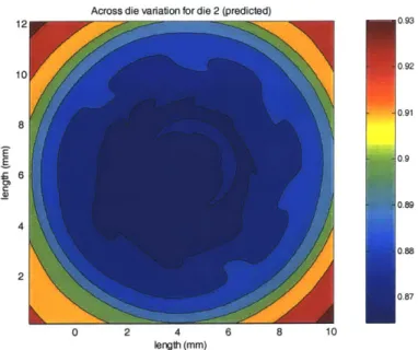
across-die variation for upper right die represents normalized etch rate.
0.92 0.91 0.9 0.89 0.88 0.87
(6.9%). The color scale
E xperimental Etch Data for Die 2
1OF
2 4 6
length (mm)
8 10 12
Figure 3-11 - Measured across-die variation for upper right die (9.2%). The color scale represents depth in microns.
8 a 4 2 275 270 265 260 255 ... . ... . .... ... -=ZM
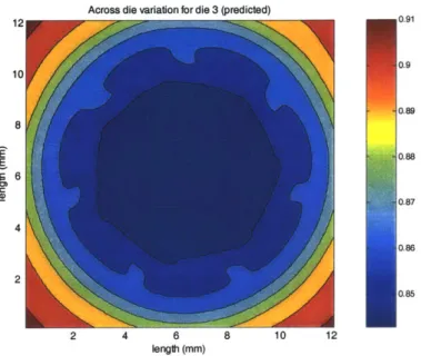
Across die variation for die 3 (predicted) E - 6 CO 4 2 length (mm)
Figure 3-12 - Simulated across die variation for the middle die represents normalized etch rate.
Experimental Etch Data for Die 3 12 11 10 9 8 7 6 5 4 3 2 1 0 2 4 6 length (mm) 8 10 12 12
I
!55 !54 ?53 ?52 ?51Figure 3-13 - Measured across die variation for center die. This die has the least variation In depth dueto the presence of balanced loading on all sides. The color scale represents
depth in microns. 7= - ;7- = ... .. ... ... . .... ... ... -... .. .... . ... all& 0.91 0.9 0.89 ( .T o 0.87 0.86
Across die variation for die 4 (Dredicted) 6 4 2 2 4 6 8 10 length (mm)
Figure 3-14 - Simulated across die variation for lower left die. normalized etch rate.
12 10 8 6 4 2 0 2 4
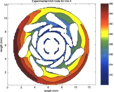
Experimental Etch Data for Die 4
6 length (mm) 8 10 12 89 0.88 0.87 12
The color scale represents
266 264 260 258 256 254 252
Figure 3-15 - Experimental etch data for the lower left die. The color scale is depth in microns. 12 8 0.93 0.92 0.91 . .. . . .. ... ..... ... ...... ... ...
12
10
8
Across die variation for die 5 (predicted)
2 4 6 8 10
length (mm)
Figure 3-16 - Simulated etch variation for lower right die. normalized etch rate.
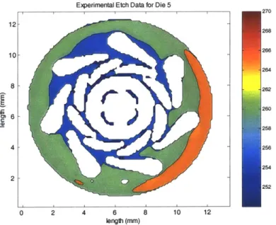
Experimental Etch Data for Die 5
12 10 8 6 4 2 0 2 4 6 8 10 12 length (mm) 0.93 0.92 0.91 0.9 0.89 0.88 0.87 12
The color scale represents
270
264
262
210
258
Figure 3-17 - Experimental etch data for lower right die. The color scale represents etched depth in microns.
As a further test, etch rate variations are also considered on a scale internal to a single die. In order to measure intra-die variation, depth measurements were taken at a 2.2 mm radius from the center of each die. Taking measurements at a constant radius minimizes
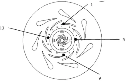
feature-level effects, since the feature opening will be similar along the circumference. The numbering scheme for these positions is shown in Figure 3-18.
1
13 1 2
9
Figure 3-18 - Measurement scheme for subsequent figures. The measurements were taken at a 2.2 mm radius for the die center.
The pattern density model is able to capture the subtle spatial pattern of etch
nonuniformity within this ring, as seen in Figure 3-19 through Figure 3-23, which show
predictions and experimental measurements for the each of the five dies in the layout.
The trends in the figure can be understood qualitatively: positions nearest to the center of
the wafer layout have a higher pattern density, and experience a slower etch rate. The
empirical scaling coefficient a is tuned to the turbopump data; without tuning, the correct
spatial trends are captured but our 1% error results in offsets in the trends of Fig. 8. The
filter magnitude tuning appears necessary to overcome model limitations. An a value of
2.34 was found to fit the data. The data was normalized by subtracting the max value
Model vs. Experimental Data (Die 1) 1.001 -0.999 0.998 0.997 0.996- 0.995-0.994 0.993-0.992 L 0 10 12 14 16
Figure 3-19 - Comparison between simulated and experimental etch rates for the upper left die. The model data is represented by squares; experimental data is in diamonds.
Model vs. Experimental Data (Die 2)
2 4 6 8
position 10 12 14 16
Figure 3-20 - Comparision between simulated and experimental etch rates for upper right die. The model data is represented by squares; experimental data is in diamonds.
N 0 z 2 4 6 8 position N -1.001 1- 0.999- 0.998- 0.997- 0.996- 0.995-0.994 0.993 Ca 'a ND 0 z A 0' N / N / 0.992 0.9911 0 . . . . I I
Model vs. Experimental Data (Die 3)
1.0005
2 4 6 8
position
10 12 14 16
Figure 3-21 - Comparision between simulated and experimental etch rates for the center die. The model data is represented by squares; experimental data is in diamonds.
Model vs. Experimental Data (Die 4)
1.001 1 -.. - -Cu a) 0 z 0.999- 0.998-0.997 0.996- 0.995- 0.994- 0.993- 0.992-0.991 0 2 4 6 8 position 10 12 14 16
Figure 3-22 - Comparison between simulated and experimental etch rates for the lower left die. The model data is represented by squares; experimental data is in diamonds.
42 z I II I I 0.9995- 0.999-0.9985 - 0.998- 0.9975-0.997 0 I I I I I I I
Model vs. Experimental Data (Die 5) 1.001 -19 0.999- 0.998- 0.997- 0.996- 0.995- 0.994- 0.993-0.992 - 0.991-10 12 14 16
Figure 3-23 - Comparison between experimental and simulated ER data for the lower right die. The model data is represented by squares; experimental data is in diamonds.
The tuning parameter allows intra-die variation to be accurately modeled. It should be
noted that it is most difficult to model intra-die nonuniformity for the center die (see
Figure 3-21) because it has the smallest range of etch rate variation. Table 3-2
summarizes the results from the turbopump demonstration.
Table 3-2 - Summary of pattern density model demonstration
Die 1 (upper left) Die ghtpper Die 3 (center) Die 4 (lower left) Die (lwer
Across die variaton 7.02% 6.90% 7.09% 6.97% 7.03% (predicted) Across die variation 6.80% 9.20% 3.90% 6.40% 8.50% (actual) RMS Error 0.09% 0.08% 0.11% 0.03% 0.08% -2? as cc zc 2 4 6 8 position I
![Figure 2-1 - Plot describing relationship between etch rate and 'loaded' area on wafer [8].](https://thumb-eu.123doks.com/thumbv2/123doknet/13964514.453148/22.918.209.743.204.504/figure-plot-describing-relationship-etch-rate-loaded-wafer.webp)