Advanced Silicon Photonics for Microwave
Frequency Down-conversion
by
Matthew Byrd
B.S., Clemson University (2015)
Submitted to the
Department of Electrical Engineering and Computer Science
in partial fulfillment of the requirements for the degree of
Master of Science in Electrical Engineering and Computer Science
at the
MASSACHUSETTS INSTITUTE OF TECHNOLOGY
June 2017
@
Massachusetts Institute of Technology 2017.
Author .
All rights reserved.
Signature redacted
...Department of Electrical Engineering and Computer Science
777
May 19, 2017
Certified by ...
Signature redacted
Michael R. Watts
Associate Professor of Electrical Engineering and Computer Science
Thesis Supervisor
Accepted by ...
Signature redacted
J
'Les iU
. KolodziejskiProfessor of Electrical Engineering and Computer Science
Chair, Department Committee on Graduate Students
JUN 23 2017
LIBRARIES
Advanced Silicon Photonics for Microwave Frequency
Down-conversion
by
Matthew Byrd
Submitted to the Department of Electrical Engineering and Computer Science on May 19, 2017, in partial fulfillment of the
requirements for the degree of
Master of Science in Electrical Engineering and Computer Science
Abstract
Microwave photonics is broadly defined as the study of optical devices operating in the microwave to millimeter wave spectrum, and interest in this field is continually driven by the need for higher electrical frequencies and larger signal bandwidths. However, electronic systems designed to meet these specifications are becoming in-creasingly challenging to create, while their microwave photonic counterparts offer a larger bandwidth, lower power consumption, higher linearity, and smaller footprint. Thus, microwave photonic systems are an attractive solution for challenging problems in the domain of high-speed electronics.
This thesis will examine a specific component of a microwave photonic system, a frequency down-converter. This device takes two electronic input signals and outputs the difference between the two input frequencies. To date, all demonstrations of a photonic microwave frequency down-converter have been based on bulk optical de-vices that limit its deployability to a real-world application due to a large footprint. However, recent advances to silicon photonic fabrication processes stand to improve the performance and enable the mass-production of many different microwave pho-tonic systems including a frequency down-converter.
In this thesis, a library of passive CMOS-compatible silicon photonic components for microwave photonic systems was developed. Additionally, a high-saturation power germanium-on-silicon photodetector showing a 70% improvement in photocurrent generation under high incident powers, and a depletion mode optical phase shifter with a VL of 0.9 Vxcm and an electro-optical bandwidth of several gigahertz were designed and tested. Finally, all of these components were assembled in a novel archi-tecture to create an integrated silicon photonic microwave frequency down-converter. Initial measurements of this structure showed an electrical-to-electrical conversion ef-ficiency of -42 dB and a suppression of spurious frequencies of approximately 15 dB. Thesis Supervisor: Michael R. Watts
Acknowledgments
First and foremost, I would like to thank my advisor, Professor Michael Watts, for the opportunity to work in the Photonic Microsystems Group. I will forever be grateful for the time spent working with some of the best minds in the field of silicon photonics and attending one of the top electrical engineering programs in the country. Thank you for not only providing an excellent laboratory stocked with all the necessary equipment, but also for your guidance and helpful insights over the past two years.
I would also like to thank the members of the Photonic Microsystems Group, both past and present. Specifically, I want to thank Christopher Poulton for taking me under his wing when I first arrived at MIT and teaching me nearly everything I know about silicon photonics. I can attribute many of my successes to the daily discussions we had during our time as officemates. In addition, I want to thank both Christopher and Cheryl Sorace for their work on initial MZM and SSB designs on which much of this thesis was based. I would also like to thank both Erman Timurdogan and Zhan Su for their mentorship. Although both were nearing graduation when I joined the group, they took time out of their days to answer my countless questions, and for that, I am extremely thankful. Finally, I would like to acknowledge the current group members, especially Manan Raval, Jelena Notaros, and Alfonso Ruocco, for their countless insightful discussions about both my project and silicon photonics in general. Thank you to all of you as this work would not have been possible without
you.
I want to also thank my parents for their constant support throughout not only my graduate career, but my whole life. Thank you for continually pushing me to higher heights by teaching me to be the best student and person that I can possibly be.
Finally, I would like to thank my wife, Kate Byrd, for beginning this journey in Boston with me. You have always believed in me even when I doubted myself. Thank you for your continued love and support, and I look forward to the rest of our lives together.
Contents
1 Introduction 23
1.1 Overview of Microwave Photonics . . . . 23
1.2 Overview of Microwave Frequency Down-conversion . . . . 24
1.3 Contributions of Present Research . . . . 27
1.4 Overview of Thesis . . . . 28
2 Passive Integrated Optical Components 29 2.1 Layers in Silicon Photonic Process . . . . 29
2.2 Integrated Waveguides . . . . 30
2.2.1 Silicon Waveguides . . . . 31
2.2.2 Silicon Nitride Waveguides . . . . 33
2.3 Input Couplers . . . . 36
2.3.1 Vertical Couplers . . . . 36
2.3.2 Edge Couplers . . . . 38
2.3.3 Input Coupler Summary . . . . 40
2.4 1x2 Splitting Devices . . . . 40 2.5 2x2 Splitting Devices . . . . 44 2.5.1 2x2 MMI Coupler . . . . 45 2.5.2 2x2 3-dB Adiabatic Coupler . . . . 46 2.5.3 2x2 Splitter Summary . . . . 48 2.6 Layer Transitions . . . . 48
3 High Saturation Power Ge-on-Si Photodetectors
3.1 Background . . . .
3.2 High-Power Saturation . . . ... . . . .
3.3 Novel Mode-Evolution-Based Input Coupler for a Reduction in High-Power Saturation . . . .
3.4
3.5
3.6 3.7
3.3.1 Coupled Local Mode Theory .
3.3.2 Coupler Design . . . . Detector Fabrication . . . . Low-power Characterization . . . . . High-power Characterization... Photodetector Summary . . . . 51 51 52 53 . . . . 54 . . . . 5 5 . . . . 5 9 . . . . 6 0 . . . . 6 3 . . . . 6 6
4 Optical Phase Shifters Based on the PlaG
4.1 Introduction to Optical Modulators . . .
4.2 Phase Shifter Design Simulation Tools 4.3 Optical Phase Shifters - First Iteration
4.3.1 Phase Shifter Design . . . . 4.3.2 Phase Shifter Fabrication . . . . . 4.3.3 Phase Shifter Measurements . . .
4.4 Optical Phase Shifters - Second Iteration 4.4.1 Phase Shifter Redesign . . . . 4.4.2 Phase Shifter Measurements . . .
sma Dispersion Effect
5 Integrated Microwave Frequency Down-converter
5.1 Parallel SSB Modulator Down-converter . . . . 5.1.1 SSB Modulator Background . . . . 5.1.2 Initial Iteration Architecture and Simulations . . . .
5.1.3 Initial Iteration Down-converter Measurements . . . . 5.1.4 Second Iteration Down-converter Simulations . . . . 5.1.5 Parallel SSB Modulator Down-converter Future Outlook
5.2 Series MZM Down-converter . . . . 67 67 . . . . 6 9 . . . . 7 2 . . . . 7 3 . . . . 7 5 . . . . 7 5 . . . . 8 4 . . . . 8 4 . . . . 8 8 93 94 94 99 102 104 105 105
5.2.1 Theoretical Background . . . . 106
5.2.2 Series MZM Down-converter Simulations . . . . 108
5.2.3 Series MZM Down-converter Measurements . . . . 109
5.2.4 Series MZM Down-converter Future Outlook . . . . 111
5.3 Photonic Down-converter Summary . . . . 112
6 Thesis Conclusion 113 6.1 Summary of Findings . . . . 113
6.2 Outlook and Future Work . . . . 114
List of Figures
1-1 Illustration of (a) up- and (b) down-conversion. . . . . 25
1-2 General diagram of the photonic-based microwave frequency down-conversion process in the frequency domain. The electrical-to-optical conversion of the (a) RF and (b) LO signals are shown, and (c) the optical-to-electrical conversion to the intermediate frequency (IF) is illustrated. . . . . 25 1-3 Block diagram illustrating a microwave frequency down-converter based
on (a) series and (b) parallel optical modulators. For each system the electrical-to-optical and optical-to-electrical conversion steps are indi-cated. ... ... ... 26
2-1 Layers available for use in this silicon photonics process including sil-icon (Si), silsil-icon nitride (SiN), germanium (Ge), routing metals, and vias. . . . . 30
2-2 Refractive index of bulk crystalline silicon plotted as a function of wavelength, which was taken from [25]. . . . . 31 2-3 (a) Illustration of a silicon waveguide surrounded by oxide (SiO2) with
width and height indicated. (b) Effective refractive index of the fun-damental TE and TM modes and the first higher-order mode in the silicon waveguide plotted as a function of waveguide width. (c) Simu-lated TE field distribution of the fundamental mode in a 400 nm wide silicon waveguide in oxide cladding. . . . . 32
2-4 (a) Illustration of the paper clip test structures. (b) Measured trans-mission through different length silicon waveguides at 1550 nm. The slope of the linear fit is the waveguide loss. . . . . 32 2-5 (a) Simulated power overlap between the fundamental TE mode in
a 400 nm wide silicon waveguide and the bend mode in this same waveguide plotted as a function of bend radius. (b) Simualted TE field distribution of the fundamental mode in a 400 nm wide silicon waveguide in oxide cladding with a 10 pm bend radius. . . . . 33 2-6 Measured refractive index of bulk silicon nitride grown in this process
with Sellmeier fit plotted as a function of wavelength. . . . . 34
2-7 (a) Illustration of a dual layer silicon nitride waveguide surrounded by oxide (SiO2) with width, height, and gap indicated. (b) Effective
refractive index of the first three modes in the dual layer silicon nitride waveguide plotted as a function of waveguide width. (c) Simulated TE field distribution of the fundamental mode in a 1.2 jim wide dual layer silicon nitride waveguide in oxide cladding. . . . . 34
2-8 (a) Transmission as a function of wavelength through three different length paper clip test structures. (b) Transmission through three dif-ferent length dual layer silicon nitride waveguides at 1550 nm. The slope of the linear fitting is the waveguide loss. . . . . 35 2-9 (a) Power overlap between the fundamental TE mode in a 1.2 Pm
wide dual layer silicon nitride waveguide and the bend mode in this* same waveguide plotted as a function of bend radius. (b) TE field distribution of the fundamental mode in a 1.2 pm wide dual layer silicon nitride waveguide in oxide cladding with a 100 pm bend radius. 36
2-10 (a) Not-to-scale illustration of the proposed grating structure. (b) Sim-ulated electric field profile of the grating coupler. (c) SimSim-ulated and measured coupling efficiency into a SMF-28 fiber as a function of wave-length . . . . 37
2-11 (a) Not-to-scale illustration of the inverse taper edge coupler. (b) Sim-ulated power overlap between the fundamental TE mode in the silicon inverse taper edge coupler and a 6.5 pm spot size lensed fiber. (c) Mea-sured coupling loss of the 140 nm silicon edge coupler as a function of wavelength. . . . . 39
2-12 (a) Simulated power overlap between the fundamental TE mode in the silicon nitride inverse taper edge coupler and a 6.5 jim spot size lensed fiber. (b) Measured coupling loss of the 300 nm dual layer silicon nitride edge coupler as a function of wavelength. . . . . 39 2-13 Not-to-scale illustration of a 1 x 2 MMI coupler with important
dimen-sions labeled. . . . . 41 2-14 Simulated and measured insertion loss of the 1 x2 silicon MMI coupler. 43
2-15 Simulated and measured insertion loss of the 1 x 2 dual layer silicon
nitride M M I coupler. . . . . 44
2-16 Not-to-scale illustration of a 2 x 2 MMI coupler with important
dimen-sions labeled. . . . . 45
2-17 (a) Simulated and measured insertion loss of the 2 x2 MMI coupler. (b) Simulated and measured power in the through and cross ports. . . 46
2-18 (a) Not-to-scale illustration of a 3-dB adiabatic splitter. (b) The
evo-lution of the input modes to the output modes. (c) Power transmission to symmetric (Sym) and antisymmetric (Anti) modes as a function of device length. . . . . 47
2-19 (a) Simulated and measured insertion loss of the 3-dB adiabatic
split-ter. (b) Simulated and measured power in the through and cross ports where the insertion loss found in (a) has been removed from the mea-sured data. ... ... 48 2-20 (a) Not-to-scale illustration of the silicon nitride to silicon escalator.
(b) Simulated and measured power transmission through the escalator
3-1 (a) Not-to-scale diagram of the mode-evolution-based coupler and a simplified Ge-on-Si detector. (b) The effective refractive index of the optical modes as a function of position in the structure using 5 pm bend radius and 10 pm taper length at a wavelength of 1550 nm. (c) Cross-sectional views of the TE electric field distribution of symmetric (Sym.) and antisymmetric (Asym.) modes and structure refractive index distribution (Struct.) at positions (1) to (4). . . . . 56 3-2 Eigenmode expansion simulation of the Ge-on-Si photodetector
illus-trating power coupled to the desired and unwanted modes as a function of taper length. ... ... 57 3-3 3D illustration of the fabricated (a) butt- and (b) mode-evolution based
coupled Ge-on-Si detectors. In (a), the 50 pm taper is not drawn to scale. . . . . 57
3-4 (a) FDTD simulation of power coupled to each mode for both cou-plers at 1520 nm. Power absorbed as a function of position for a
1.5 pmx12 pm Ge-on-Si photodetector using the (b) butt- and (c)
mode-evolution-based coupler at 1520 nm (k = 0.045) [66]. . . . . 58 3-5 Not-to-scale illustration of a top-down view of a 1.5 pmx12 pm
fab-ricated Ge-on-Si photodetector with both butt- and mode-evolution-based coupled inputs. Critical device dimensions are labeled in the
sketch... ... 60
3-6 Measured IV characteristics of the 1.5 pmx 12 jim and 4.0 pmx 12 pm
sized photodetectors, which are independent of input coupler type. . . 61 3-7 Measured responsivity of 1.5p mx12pm and 4jimx 12pm Ge-on-Si
pho-todetectors as a function of input wavelength with an 80AfW TE-polarized optical input. . . . . 62 3-8 (a) Block diagram of optical heterodyne experiment used to measure
the frequency response of the Ge-on-Si photodetectors. (b) Measured frequency response of the 1.5 jimx 12 pm Ge-on-Si detector with a total of 20 pm of TE-polarized optical input power normalized at 300 MHz. 63
3-9 Measured photocurrent generation as a function of 1550 nm TE-polarized
optical input power to the 1.5 pmx12 pm detector for both butt- and mode-evolution-based couplers. The inset plots the low-power data points on a logarithmic scale to demonstrate the high dynamic range of this device, which spans roughly six orders of magnitude. . . . . . 64
3-10 Measured frequency response of the 1.5 pmx 12 pm Ge-on-Si
photode-tector with each coupler type at 20 jiW (red and blue curves) and 4 mW (black and green curves) 1550 nm TE-polarized total optical input pow er. . . . . 65
4-1 Illustration showing two different types of p-n junctions: (a) lateral and (b) vertical. . . . . 68
4-2 Illustration showing two p-n junction optical phase shifters inside an on-chip Mach-Zehnder interferometer. . . . . 69
4-3 Example output from an Sprocess module in Synopsys Sentaurus mod-eling software showing the structure and doping concentration of a vertical p-n junction phase shifter . . . . 69
4-4 Example output from an Sdevice module in Synopsys Sentaurus mod-eling software showing the free-carrier concentration of a vertical p-n junction at (a) 0 V and (b) 6 V reverse bias. The white lines denote
the depletion region of the p-n junction. . . . . 70
4-5 Example output from MATLAB processing code showing the change in (a) effective refractive index, Aneff, and (b) optical loss through the p-n junction as a function of reverse bias voltage. . . . . 71
4-6 (a) Example output from Sdevice capacitance simulation. (b) Example output from Sdevice voltage step simulation with fit to a 60.5 GHz bandwidth decaying exponential function. . . . . 72
4-7 (a) Final simulated structure of the first iteration of the vertical p-n junction. Simulated (b) Aneff and (c) optical insertion loss as a function of reverse bias voltage. (d) Simulated device capacitance as a function of reverse bias voltage and input frequency. (e) Simulated p-n junction response to a 0.1 V step function at 3 V reverse bias (solid curve) and decaying exponential fit (points). . . . . 74
4-8 (a) Block diagram of the experimental setup used to measure the DC characteristics of the optical phase shifters. (b) The measured power in the through and cross ports for 1, 2, and 3 mm long phase shifters. 78
4-9 (a) Measured and simulated Aneff (V) of the 1, 2, and 3 mm optical phase shifters. (b) Measured phase change of the 1, 2, and 3 mm phase shifters. (c) Measured optical transmission through the Mach-Zehnder modulators at 0 V applied bias and fit to find optical loss through the p-n junction. (d) Measured and simulated La (V) of the 1, 2, and
3 mm optical phase shifters. . . . . 79
4-10 Block diagram of the experimental setup used to measure the high-speed characteristics of the optical phase shifters. . . . . 80
4-11 Received RF power at the electrical spectrum analyzer as a function of frequency (a) before and (b) after the calibration of the function generator, bias tee, and RF cable. . . . . 81
4-12 Measured frequency response of the (a) XPRV 2021 photoreceiver and
(b) commercial LiNbO3 modulator. . . . . 82
4-13 (a) Measured electro-optical response of the vertical p-n phase shifters of various lengths at 0 V reverse bias. (b) Measured electro-optical response of the 0.5 mm phase shifter at several reverse bias voltages. . 83
4-14 (a) Simulated depletion region location at (top) 0 V reverse bias and (bottom) 6 V reverse bias of the first generation vertical p-n junction.
(b) Simulated voltage step (from 5 V to 6 V) response of this junction
(solid curve) and decaying exponential fit (points) as a function of ridge thickness. (c) Simulated (c) Aneff and (d) junction loss as a function of reverse bias voltage and ridge thickness. . . . . 85
4-15 Simulated (a) Aneff and (b) optical insertion loss as a function of reverse bias voltage and doping concentration. . . . . 86
4-16 (a) Final simulated structure of the second generation vertical p-n junc-tion. Simulated (b) Aneff and (c) optical insertion loss as a function of reverse bias voltage. (d) Simulated device capacitance as a function of reverse bias voltage and input frequency. (e) Simulated p-n junction response to a 0.1 V step function at 3 V reverse bias (solid curve) and decaying exponential fit (points). . . . . 87
4-17 (a) Measured and simulated Aneff (V) of the 1, 2, and 3 mm phase shifters. (b) Measured phase change of the 1, 2, and 3 mm p-n junc-tions. (c) Measured optical transmission through the Mach-Zehnder modulators at 0 V applied bias and fit to find optical loss through the p-n junction. (d) Measured and simulated Aa (V) of the 1, 2, and
3 m m phase shifters. . . . . 89
4-18 (a) Measured electro-optical response of the phase shifters of various lengths at 0 V reverse bias. (b) Measured electro-optical response of the 0.5 mm vertical p-n junction phase shifter at several reverse bias voltages. . . . . 90 5-1 Basic SSB modulator architecture with the frequency domain
illustra-tions of key steps. In this image, phase modulators are represented by
p where -p indicates a 180* out of phase modulation (i.e. push-pull
configuration). Static phase shifts are represented by the 7r and 7r/2 blocks. . . . . 94
5-2 Conversion efficiency from the carrier signal to the first, third, and fifth
harmonics in the SSB modulator using the derived expression for the output optical field. . . . . 98 5-3 Simulated conversion efficiency from the carrier signal to the first,
third, and fifth harmonics in the SSB modulator using the model equa-tions for the p-n juncequa-tions from Chapter 4. . . . . 99
5-4 Illustration of the parallel SSB type photonic down-converter with fre-quency domain plots at several key points in the structure. In this image, phase modulators are represented by a, static phase shifts are shown by the r and 7/2 blocks, the 2 x 2 block is a 2 x 2 optical power splitter, and PD is a photodetector. . . . . 100 5-5 Simulated output from the first iteration of the parallel SSB modulator
photonic down-converter with (a) 0.95 GHz and (b) 0.17 GHz RF signal with 0.14 GHz and 0.92 GHz IF outputs, respectively. . . . . 101 5-6 Optical micrograph of the fabricated SSB modulator type photonic
microwave frequency down-converter. . . . . 102
5-7 Measured output from the first iteration of the parallel SSB modulator
type photonic down-converter with (a) 0.95 GHz and (b) 0.17 GHz RF signal with 0.14 GHz and 0.92 GHz IF outputs, respectively. . . . . . 103 5-8 Simulated output from the second iteration of the parallel SSB
modula-tor type photonic down-converter with (a) 0.95 GHz and (b) 0.17 GHz
RF signal with 0.14 GHz and 0.92 GHz IF outputs, respectively. . . . 104
5-9 Schematic of the architecture and operation of the series MZM
down-converter with frequency domain illustrations at key points in the struc-ture. In this image, phase modulators are represented by o, static phase shifts are shown by the ir and </2 blocks, the 2 x 2 block is a 2 x 2 optical power splitter, and PD is a photodetector. . . . . 106 5-10 Simulated output from the series MZM type photonic down-converter
with 0.44 GHz RF signal, 0.49 GHz LO frequency, and a 0.05 GHz IF
5-11 Optical micrograph of the fabricated series MZM modulator type
pho-tonic microwave frequency down-converter. . . . 110
5-12 Measured output from the series MZM type photonic down-converter
(a) without and (b) with an electrical filter on the output. . . . . 110 5-13 Measured (a) 1-dB compression point and (b) 11P3 of the series MZM
List of Tables
2.1 Optimized parameters for the 1 x2 silicon MMI coupler. . . . . 42 2.2 Optimized parameters for the dual layer 1 x 2 silicon nitride MMI coupler. 43
2.3 Optimized parameters for the 2 x2 silicon MMI coupler. . . . . 45 2.4 Parameters for final 3-dB adiabatic splitter design. . . . . 47
Chapter 1
Introduction
1.1
Overview of Microwave Photonics
Microwave photonics is broadly defined as the study of optical devices and systems operating at microwave to millimeter wave frequencies. This field continues to be driven by the constant need for higher frequencies for baseband transmission and larger bandwidths for encoded information. These requirements are often complex or impossible for current electronic systems to achieve [1, 21. Therefore, the goal of microwave photonics is to exceed the boundaries of conventional high-speed elec-tronics by leveraging a different region of the electromagnetic spectrum. Using this technology, microwave photonic implementations of electronic systems at the higher end of the radio frequency (RF) spectrum, such as wireless networks, sensors, radar, and satellite communications, can be driven to even higher frequencies and larger bandwidths exceeding the performance of state-of-the-art electronics [3].
In the 1970's, it became clear that copper wiring inside coaxial cables was near-ing the limits of its data carrynear-ing capacity, and the industry began looknear-ing for an alternative solution [4]. Intense efforts focused on developing the key components for an optical communication network such as external intensity modulators [5], di-rectly modulated semiconductor laser diodes [6], low loss and dispersion single-mode optical fibers [7], and high-speed photodetectors [8]. As the performance of each
individual device improved, optical links became a commercially viable solution to replace conventional copper-based electrical communication networks enabling faster and more reliable communications. After it was clear that photonics revolutionized the telecommunications industry, the field of microwave photonics began to expand to other applications in the RF domain. Besides low loss data transmission, it was discovered that microwave photonic devices provide a number of important advan-tages over electrical systems including: smaller footprint, larger bandwidth, lower power consumption, higher linearity, and better immunity to electromagnetic inter-ference [1]. One of the most attractive attributes is the large bandwidth afforded by a microwave photonic system allowing a single device to operate over several decades of the RF spectrum, which is nearly impossible using conventional electronic circuits [2].
Today, microwave photonic systems perform a variety of different functions includ-ing transmission, processinclud-ing, generation, and mixinclud-ing of microwave to millimeter wave signals [3]. While fiber-based optical transmission systems are a well known commer-cially viable solution, other applications for microwave photonic systems have not yet reached this level of maturity [11. For example, research is still being conducted in the area of signal processing to develop all-optical filters for microwave frequencies and arbitrary waveform generators with bandwidths exceeding tens of gigahertz
[9J.
Additionally, other efforts have focused on signal generation with a recent demonstra-tion showing stable microwave frequencies from 1 to 112 GHz [10]. Finally, another ongoing area of research is all-optical microwave and millimeter wave frequency up-and down-conversion [11, 12], which is the focus of this work.
1.2
Overview of Microwave Frequency
Down-conversion
Photonic microwave frequency conversion has been extensively studied because many different electrical systems require both an up- and down-converter for the microwave signals. One example of this scenario is when a data sequence is up-converted, Fig.
1-(a)
0
a-Up-conversion (b) Down-conversion
ALow Frequency High Frequency Low Frequency High Frequency
Signal /Signal Signal Signal
0
Frequency fLO Frequency fLO
Figure 1-1: Illustration of (a) up- and (b) down-conversion.
1(a), to a higher frequency for transmission and then down-converted, Fig. 1-1(b), at the receiver for further signal processing [1]. This frequency conversion is typically necessary because signal processing is more easily performed at lower frequencies while higher frequencies tend to propagate further. The photonic down-converter, however, is of particular interest because it can be applied to many high-speed systems other than data transmission [131. This general photonic-based down-conversion process is illustrated in Fig. 1-2. First, the electrical RF and local oscillator (LO) signals are converted to the optical domain, as shown in Fig. 1-2(a) and Fig. 1-2(b), respectively.
(a) Electrical-to-Optical Conversion
(c) Optical-to-Electrical Conversion
RF laser laser RF Frequency
(b): :
f1F fLOfRF laser RF laser LO
Frequency
fLO flaser flaser fLO
Frequency
Figure 1-2: General diagram of the photonic-based microwave frequency down-conversion process in the frequency domain. The electrical-to-optical down-conversion of the (a) RF and (b) LO signals are shown, and (c) the optical-to-electrical conversion to the intermediate frequency (IF) is illustrated.
Then, these two optical signals are mixed and beat on a photodetector converting optical energy back to the electrical domain, as shown in Fig. 1-2(c) [13]. A much more thorough mathematical description of the full microwave frequency down-converter is included in Chapter 5.
Overall, the photonic frequency down-converters demonstrated to date follow the same general key steps, which can be implemented in two different configurations.
Both are shown in Fig. 1-3. In the series modulator configuration, Fig. 1-3(a), the RF microwave signal is converted to the optical domain by modulating a laser source with an optical modulator. Then this signal is passed through another electro-optical modulator driven at the LO frequency. Finally, these two microwave frequen-cies are mixed by converting the optical signal to the electrical domain on a pho-todetector resulting in the generation of the desired intermediate frequency (IF), or the difference between RF and LO frequencies [13-21]. In the parallel modulator down-converter, Fig. 1-3(b), the input laser is split equally into two arms. The laser in each arm passes through an electro-optical modulator. One modulator is driven
by the RF signal, and the other by the LO signal. These two modulated signals are
then combined and mixed on a photodetector generating the desired IF output [2]. To meet the demands of today's high-performance systems, these photonic-based down-converters have been developed with the goal of increasing bandwidth, decreas-ing cross-talk, and increasdecreas-ing linearity compared to their electrical counterparts [12]. Previous work in this area has shown how to reduce conversion losses [14-171 and increase dynamic range [18, 19] of photonic frequency down-converters using these
(a) (b) RF
RF LO IFModulator IF
Laser H. Modulator H Modulatoaj sr LO Photodetectorl
Electrical-to-Optical Optical-to-Electrical
Modulator Optical-to-Electrical Electrical-to-Optical
Figure 1-3: Block diagram illustrating a microwave frequency down-converter based on (a) series and (b) parallel optical modulators. For each system the electrical-to-optical and electrical-to-optical-to-electrical conversion steps are indicated. .
two architectures. Other work has detailed the importance of the local oscillator by showing great improvements in phase noise performance when using an extremely high spectral purity LO [121. Furthermore, others have taken advantage of optical multi-plexing techniques to down-convert multiple signals simultaneously within the same structure. These techniques often leverage the fact that the optical components used in the microwave frequency down-converter system have a similar level of performance over a wide range of optical wavelengths and polarizations. For example, in [20,21], signals carried on separate wavelengths were simultaneously down-converted to the IF exploiting the wavelength division multiplexing property of light. In [131, a similar experiment was performed; however, this data was encoded in different polarization states of the input light. Such experiments have served to further show the advantages of a photonic-based microwave frequency system.
1.3
Contributions of Present Research
Although promising, the aforementioned microwave frequency down-converters have been based on bulk optical devices such as laser diodes, lithium niobate optical modu-lators, erbium-doped fiber amplifiers, and stand-alone photodetectors, which are often secured to large optical tables. Their size makes these systems unwieldy and limits their deployability to real-world applications. To decrease system footprint and en-able mass-production, microwave photonics systems using bulk optics, optoelectronic devices, and optical fiber can be redesigned on a wafer-scale integrated platform with the silicon-based complementary metal-oxide-semiconductor (CMOS) compatible pro-cesses used to fabricate microprocessors, memory, and solid-state drives. Leveraging the years of knowledge developing nanometer scale transistors will enable the design and fabrication of high-quality silicon photonic integrated circuits, which can easily be combined with wafer-scale CMOS-based electronics [22]. In the context of microwave photonic down-conversion, the modulators and photodetectors can be moved on-chip and connected with low-loss silicon waveguides to decrease both size and cost while increasing the performance and enabling mass-production of these systems.
Thus, the focus of this thesis was to first develop the necessary integrated opti-cal components, such as waveguides, photodetectors and modulators, to recreate the microwave frequency down-converter based on bulk optical devices. Then, using mea-sured performance-based models of these integrated components, the down-converter architecture was improved in order to maximize the performance of this integrated optical system. Finally, this novel integrated microwave frequency down-converter was fabricated and tested.
1.4
Overview of Thesis
In the following chapters of this thesis, the design of an integrated silicon photonic microwave frequency down-converter will be described. Chapter 2 details the design of several integrated passive optical components necessary for the down-converter de-sign including optical waveguides, fiber-to-chip couplers, and power splitters. Several different types of each component were examined and the best performing were chosen for the final down-converter design. Chapter 3 describes the design of a high-power in-tegrated germanium photodetector for the optical-to-electrical conversion step in the microwave frequency down-converter. This component was optimized to maintain a similar level of performance up to incident powers on the order of several milliwatts. In Chapter 4, the design of an integrated depletion mode optical phase shifter is presented for the electrical-to-optical conversion step. An existing phase shifter was tested, and then, the design was improved to better meet the specifications of the microwave frequency down-converter. Finally, Chapter 5 describes the design, simu-lation, and measurement of two different configurations of an integrated microwave frequency down-converter. While both designs produce the desired IF output, there are various trade-offs between device complexity and performance that are discussed within this chapter.
Chapter 2
Passive Integrated Optical
Components
The microwave frequency down-converter required the design of several passive com-ponents including optical waveguides, fiber-to-chip input couplers, and power splitting devices. This chapter discusses the advantages and disadvantages of the most common approaches to each of these components. First, silicon and silicon nitride waveguides are compared. Then, vertical grating couplers are compared to inverse tapered edge couplers. Finally, 1 x 2 power splitters such as multi-mode interference (MMI) cou-plers, directional coucou-plers, and Y-junctions and 2 x 2 power splitters including MMI couplers and 3-dB adiabatic splitters are discussed. The best performing device in each category was chosen for the final design of the integrated microwave frequency down-converter.
2.1
Layers in Silicon Photonic Process
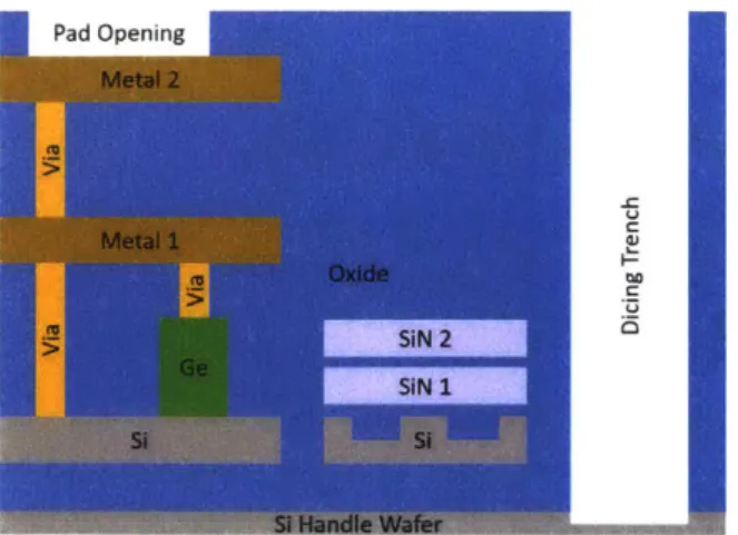
This work utilized the 300 mm wafer silicon photonics platform at the Colleges of Nanoscale Science and Engineering (CNSE) at the SUNY Polytechnic Institute in Albany, New York. This silicon photonics process contains a number of layers that can be used to create complex integrated photonic systems such as the microwave
Pad Openg
C
5J
SiN 1
Si-Figure 2-1: Layers available for use in this silicon photonics process including silicon (Si), silicon nitride (SiN), germanium (Ge), routing metals, and vias.
frequency down-converter. A not-to-scale cross-sectional view of these layers is shown in Fig. 2-1. In this process there are three different layers for low loss guiding of light: one silicon and two silicon nitride. There is also a germanium layer that is used for light detection, and finally, there are two metal layers with vias that can be used for routing of electrical signals.
In addition to all of the layers shown in Fig. 2-1, this process contains several different n- and p-type dopants for implantation into the silicon. These dopants can be used to create active optical devices and will be discussed in the subsequent chapters. For the final design of the microwave frequency down-converter, all of these layers will be required in order to fabricate the necessary subcomponents of the overall system.
2.2
Integrated Waveguides
One of the most important features of an integrated photonic circuit is the waveguide used for routing optical signals. The dimensions of the waveguide must be properly selected to maintain single-mode operation while providing adequate confinement for the optical mode. The fabrication process used to make these integrated optical devices contains two different materials that can be used as waveguides: silicon and silicon nitride. Both are viable options to guide light with low loss and current
research has shown total propagation losses lower than 10 dB/m for highly confined modes in both silicon [231 and silicon nitride [24]. In the subsequent subsections, each material in this process will be examined for guiding light on-chip.
2.2.1
Silicon Waveguides
Silicon is one of the most common materials used for integrated photonic systems due to the decades of research spent developing fabrication techniques for microprocessors, memory, and solid-state drives. These processes can be directly applied to make integrated silicon photonic circuits, which can operate at wavelengths spanning from roughly 1100 nm to the far-infrared [251. The refractive index of bulk silicon is plotted as a function of wavelength in Fig. 2-2 over part of this range.
To design the single-mode waveguide shown in Fig. 2-3(a), a target wavelength must first be selected. In this case, the telecommunications wavelength of 1550 nm was chosen because high-power optical sources near this wavelength are readily available. As the height of the silicon layer is fixed at 220 nm in the fabrication process, the only other parameter left to choose was the width of the waveguide. This parameter was chosen such that the integrated waveguide tightly confined the fundamental transverse electric (TE) optical mode. To find the width that achieved maximum confinement while maintaining single-mode operation, the effective refractive indices at 1550 nm of the fundamental TE, fundamental transverse magnetic (TM), and first higher order
3.52 3.50 X nD=n3.745 at 1550 nm 3.48 3.44 3.42 1000 2000 3000 4000 Wavelength [nm]
Figure 2-2: Refractive index of bulk crystalline silicon plotted as a function of wave-length, which was taken from [251.
(a) (b) 2.8 (c)-2 1.0 X Q TE SiO2 24- TMn 0.8 Wdt TE '--n =2.23at1550 nmn. Width t eff 0.6 1:2.0 0.4 CU7 220 nm 1.61 .. 2 0.2 1.2 - 2 0.0 200 400 600 800 -2 -1 0 1 2 Waveguide Width [nm] x [pm]
Figure 2-3: (a) Illustration of a silicon waveguide surrounded by oxide (SiO2) with width and height indicated. (b) Effective refractive index of the fundamental TE and TM modes and the first higher-order mode in the silicon waveguide plotted as a function of waveguide width. (c) Simulated TE field distribution of the fundamental mode in a 400 nm wide silicon waveguide in oxide cladding.
mode were simulated and plotted in Fig. 2-3(b). From this plot, it can be seen that a width of 400 nm maximally confined the fundamental TE mode while maintaining single-mode operation. The simulated TE mode field profile in this final waveguide design is shown in Fig. 2-3(c).
To characterize this integrated silicon waveguide, light at a wavelength of 1550 nm was input into different length waveguides. These structures, known as paper clips, are commonly used to measure waveguide loss and are illustrated in Fig. 2-4(a). The
(a) (b) -9.6 _ 9.8 --1.52 dB/cm 0 -10.0 - -Q1 12141,1 E C F-% -10.4--10.6 10 12 14 16 18 Waveguide Length [mm]
Figure 2-4: (a) Illustration of the paper clip test structures. (b) Measured transmis-sion through different length silicon waveguides at 1550 nm. The slope of the linear fit is the waveguide loss.
(b) 1.00 1-2 1.0 99.9% at 10 pm 0.8 c.0.98- -1 d-, 0.6 >U E O0.96- 00.6 0.4 13- 0.941 . S 0.2 0.92 2 0.0 0 10 20 30 -2 -1 0 1 2 Bend Radius [pm] x [pm]
Figure 2-5: (a) Simulated power overlap between the fundamental TE mode in a 400 nm wide silicon waveguide and the bend mode in this same waveguide plotted as a function of bend radius. (b) Simualted TE field distribution of the fundamental mode in a 400 nm wide silicon waveguide in oxide cladding with a 10 Jim bend radius. transmission through each paper clip was measured and plotted as a function of waveguide length in Fig. 2-4(b). The slope of this line is the waveguide loss, which was found to be 1.52 dB/cm. Such a low propagation loss will enable the development of efficient optical systems based in this silicon layer, which is critical for the success of the microwave frequency down-converter.
The final important parameter for the integrated silicon waveguide is the minimum bend radius such that the power overlap between the optical mode in the straight waveguide and bent waveguide is near unity. A plot of this simulated power overlap versus bend radius is shown in Fig. 2-5(a). As the optical mode is tightly confined in the silicon waveguide, this bend radius can be very small. A bend radius of 10 Pm yielded a power overlap of greater than 99.9%. The simulated TE field profile of the optical mode in the bent waveguide is shown in Fig. 2-5(b) and was nearly identical to that shown in Fig. 2-3(c), which is the straight waveguide.
2.2.2
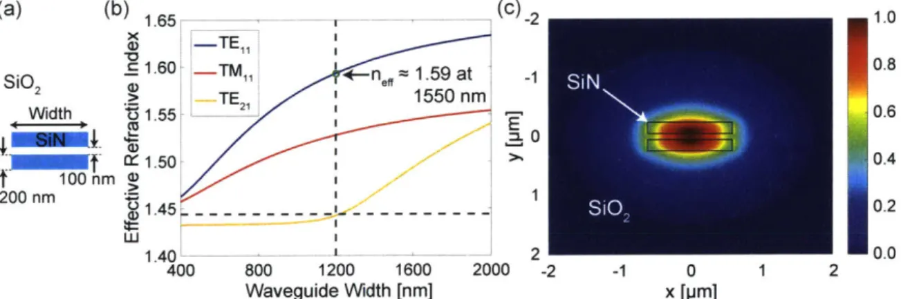
Silicon Nitride Waveguides
Silicon nitride is another common material for optical routing on-chip due to its large transparency window spanning from the visible wavelengths to the near-infrared, low propagation loss, and high power handling capabilities [261. The process discussed in Section 2.1 contains two silicon nitride layers that can be used for routing. The
2.2 - _ _ _ _ _ _----~---Sellmeier Fit SMeasured Data 02.1 n= 1.95 at 1550 nm c 2.0 1.9 400 800 1200 1600 2000 Wavelength [nm]
Figure 2-6: Measured refractive index of bulk silicon nitride grown in this process with Sellmeier fit plotted as a function of wavelength.
refractive index of silicon nitride is highly dependent upon the process used to grow the layer, and the refractive index of bulk silicon nitride grown in this process is plotted as a function of wavelength in Fig. 2-6.
Again, the height of these two silicon nitride layers is fixed at 200 nm, and thus, at an input wavelength of 1550 nm, a single layer of silicon nitride does not tightly confine the optical mode. Due to the buried oxide thickness of 2 Pm, this optical mode in a single layer of silicon nitride will see the substrate inducing unwanted loss. Thus, both silicon nitride layers must be used to more tightly confine the optical mode. Using the waveguide geometry shown in Fig. 2-7(a), a waveguide width of 1.2 Pm
(a) (b) 1.65 _ _ _ (c) -2 1.0 .)X -TE1 SO 1.601 TM1e, 1. 59 at N 0.8 2 > -TE 1550 nm Width 1.55 - 0.6 0. Xf 1.50' 0.4 f 100 nm 0 200 nm1 1.45 --- --- SO 0.2 1.401 2 10.0 400 800 1200 1600 2000 -2 -1 0 1 2 Waveguide Width [nm] x [pm]
Figure 2-7: (a) Illustration of a dual layer silicon nitride waveguide surrounded by oxide (SiO2) with width, height, and gap indicated. (b) Effective refractive index of
the first three modes in the dual layer silicon nitride waveguide plotted as a function of waveguide width. (c) Simulated TE field distribution of the fundamental mode in a 1.2 pm wide dual layer silicon nitride waveguide in oxide cladding.
was chosen for maximal confinement with single-mode operation. A simulation of the effective refractive indices of the first three supported modes is shown in Fig.
2-7(b) again illustrating this choice of width. Additionally, the simulated TE field
distribution of the final mode is plotted in 2-7(c).
Again, the waveguide loss was measured using paper clip test structures. The measured transmission through these structures is plotted as a function of wavelength for three different device lengths in Fig. 2-8(a), and as a function waveguide length at a wavelength of 1550 nm in Fig. 2-8(b). For a waveguide width of 1.2 Pm at a wavelength of 1550 nm, the propagation loss was determined to be 2.88 dB/cm. This value is higher than silicon in part due to the increased absorption at 1520 nm, which is commonly observed in silicon nitride films [27]. However, this propagation loss was still low enough for use in the microwave frequency down-converter.
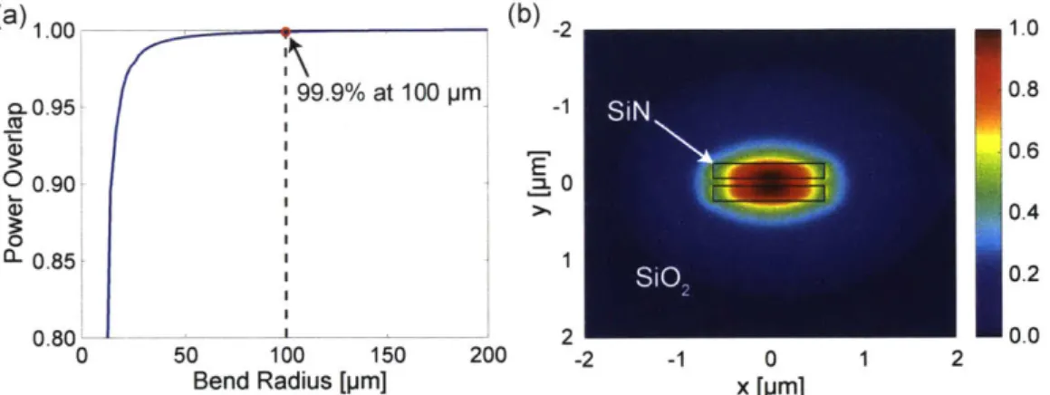
Finally, the minimum bend radius of the dual silicon nitride waveguide was de-termined in the same manner as the silicon waveguide. A plot of this power overlap versus bend radius is shown in Fig. 2-9(a) with the TE field profile of the fundamental optical mode in the bent waveguide shown in Fig. 2-9(b). The minimum bend radius was significantly larger than that of the silicon waveguide because the mode was much less confined in this material.
(a) (b) -8 -12.6 -10 -- 12.8--12. -2.88 dB/cm M -13.2 % C --12 - 0 . m M -13.2 --14 . m C -1 12.5 mm %% -1 -14.3 mm -13.6- % I 16.0 mm -18 ' ' -13.8 1.5 1.52 1.54 1.56 1.58 1.6 12 13 14 15 16 17
Wavelength [pm] Waveguide Length [mm]
Figure 2-8: (a) Transmission as a function of wavelength through three different length paper clip test structures. (b) Transmission through three different length dual layer silicon nitride waveguides at 1550 nm. The slope of the linear fitting is the waveguide loss.
(a) 1.0 0 (b) -2 1.0 0.0.94 99.9% at 100 pm -1 0.8 - 0.6 0.90.6 0.4 0 0.851 1 0.2 0.80 2 0.0 0 50 100 150 200 -2 -1 0 1 2 Bend Radius [pm] x [pm]
Figure 2-9: (a) Power overlap between the fundamental TE mode in a 1.2 Pm wide dual layer silicon nitride waveguide and the bend mode in this same waveguide plotted as a function of bend radius. (b) TE field distribution of the fundamental mode in a 1.2 pm wide dual layer silicon nitride waveguide in oxide cladding with a 100 um bend radius.
2.3
Input Couplers
With the optimal design for an on-chip waveguide determined, the next step was to engineer a coupling scheme to efficiently transfer light from a fiber to the on-chip waveguide. This task is relatively challenging because of the small size of the integrated waveguides. In addition, the high refractive index contrast of the silicon waveguide makes matching the effective indices of the two optical modes difficult [28]. To solve these challenges, two main approaches are used to couple light onto the chip: vertical and edge couplers. In the subsequent sections, both approaches will be explored to determine the optimum coupler for use in the microwave frequency down-converter.
2.3.1
Vertical Couplers
Vertical grating couplers are commonly used in the field of silicon photonics to couple light into on-chip single-mode waveguides because this type of structure is compatible with wafer-scale testing and established packaging technologies
[291.
However, fiber-to-chip coupling efficiencies using vertical grating couplers have historically been low due to mode mismatch and power loss to the substrate [281. These problems havebeen solved by using apodization techniques [301 and mirrors under the grating [311, both of which increase fabrication complexity.
However, another solution to the substrate power loss problem is to engineer the radiation from the grating to emit only in the upward direction. With two different etch depths in silicon, the radiation from these two trenches can be designed to interfere constructively in the upward direction (towards the fiber) and destructively in the downward direction (towards the substrate). This result was first simulated in
[32] and then fabricated using a slightly different design in [28]. However, the gratings
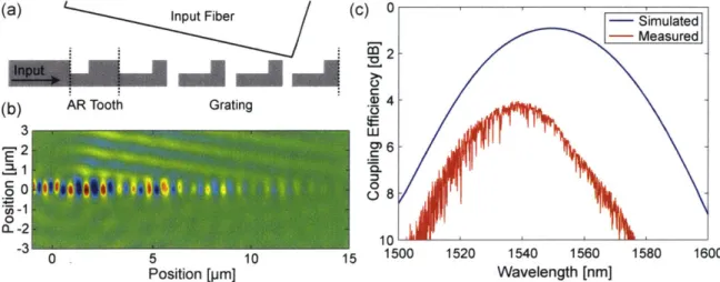
demonstrated in [28] use electron-beam lithography instead of 193 nm immersion lithography and utilize a shallow, 70 nm deep, etch not present in the process. Thus, this type of grating coupler was redesigned with a deeper 120 nm etch in the silicon layer with features large enough to be fabricated using 193 nm immersion lithography. The new proposed design is illustrated in Fig. 2-10(a). The first period of this grat-ing, called an anti-reflection (AR) tooth, was specifically designed for index matching to reduce back reflections as is done in [281. With liberal use of a 2D finite-difference time-domain (FDTD) simulation in an optimization routine, each period of the grat-ing was modified to match the radiated field to that of the fiber mode as best as possi-ble. The simulated radiated electric field is plotted in Fig. 2-10(b), and from this plot it can be seen that more optical power radiated upwards than downwards.
Specifi-(a) Input(C) F Input F (b) AR Tooth Grating -D 4 3 w E G-CAI~UWAUItW 0 0 3_- 10 -3 0 5 10 15 1500 1520 1540 1560 1580 1600 Position [pm] Wavelength [nm]
Figure 2-10: (a) Not-to-scale illustration of the proposed grating structure. (b) Simu-lated electric field profile of the grating coupler. (c) SimuSimu-lated and measured coupling efficiency into a SMF-28 fiber as a function of wavelength.
cally, 92.6% of the optical power radiated upward while only 3.1% radiated downward. Finally, the coupling efficiency into a standard SMF-28 fiber with a 10.4 Pm mode field diameter was simulated and measured as a function of wavelength. The results are shown in Fig. 2-10(c). The simulation indicates that this grating has a maximum coupling efficiency of -0.92 dB and a 1 dB bandwidth of approximately 40 nm, which is comparable with the current state-of-the-art grating couplers.
2.3.2
Edge Couplers
Another type of input coupling scheme, called edge coupling, transfers light directly from the fiber to the waveguide on the edge of the chip. Typically, the on-chip single-mode waveguide is symmetrically inverse tapered to a smaller size in order to expand the guided optical mode to a size similar to that of the input fiber [33J. An alternative to the inverse taper method is to design a subwavelength structure, or metamaterial, to both expand the size and match the effective refractive index of the on-chip guided mode to the fiber mode. This metamaterial-based input coupler enables the highly efficient transfer of power into the on-chip waveguide [34]. A key advantage to this type of coupling method is that it offers low coupling loss over a broad range of input wavelengths, whereas vertical grating couplers typically have a 1 dB bandwidth of roughly 30 to 50 nm [28].
The inverse taper type edge couplers were investigated because of the simplicity of their design, as shown in Fig. 2-11(a). Again, due to the fixed layer heights, the only remaining design parameter in this structure was the final width of the inverse taper. This width was chosen to best match the field profile of the guided on-chip mode to that of the input fiber, which in this case was a 6.5 llm spot size lensed fiber. For the silicon layer, the simulated power overlap between these two modes is plotted as a function of inverse taper width in Fig. 2-11(b), and from this plot, it can be seen that optimum coupling was achieved at a width of 140 nm. The edge coupler loss was measured through a straight waveguide and the waveguide loss was subtracted from the measurement. These results are plotted as a function of input wavelength in Fig. 2-11(c) where the input coupling loss was approximately 1.81 dB at a wavelength
(a) Input Fiber ---(b) 1.0 0.8 0.6 0 0.4 0.2r 0.01 5 0 100 150 200 250 Waveguide Width [nm] (C) -1.5 -1.6 -1.8 0 0 o -2.1 300 * I * I 1520 1540 1560 Wavelength [nm]
Figure 2-11: (a) Not-to-scale illustration of the inverse taper edge coupler. (b) Sim-ulated power overlap between the fundamental TE mode in the silicon inverse taper edge coupler and a 6.5 pm spot size lensed fiber. (c) Measured coupling loss of the 140 nm silicon edge coupler as a function of wavelength.
of 1550 nm.
This design process was repeated for the dual silicon nitride waveguide. The simulated power overlap is plotted as a function of inverse taper width in Fig. 2-12(a), which shows that an optimum coupling was achieved at a width of 280 nm. The measured coupling loss is plotted as a function input wavelength in Fig. 2-12(b)
200 300 400 Waveguide Width [nm] 500 6 (b) ~0 CL 0 -0 0 -2.2 --2.3 -2.4 -2.5 -2.6 -2.7 -2.8 -2.9 -3.0 -3.1 -3.2 1500 1520 1540 1560 1580 Wavelength [nm]
Figure 2-12: (a) Simulated power overlap between the fundamental TE mode in the silicon nitride inverse taper edge coupler and a 6.5 pm spot size lensed fiber. (b) Measured coupling loss of the 300 nm dual layer silicon nitride edge coupler as a function of wavelength. -2.2 1500 0 0 0 0 0 0 0 1580 1600 (a) 1.0 0.8 S0.6 0.4 LL 0.2 0.01 100 0 0 0 0 0 0 0 1600 . - . I
and was approximately 2.47 dB at a wavelength of 1550 nm.
2.3.3 Input Coupler Summary
Although the simulated gratings demonstrated the lowest coupling loss, the inverse taper type input couplers were chosen for the final down-converter design due to their broadband operation, ease of fabrication, and acceptably low loss. From the measure-ment results of the uni-directional grating couplers, it can be seen that fabrication errors can have a large impact on the performance of this structure, which also led to the decision to use edge couplers. Additionally, the final down-converter design used the dual layer silicon nitride edge couplers due to their superior high-power operation compared to silicon waveguides (as discussed in Section 2.2.2). However, silicon-based inverse taper edge couplers were used on most of the test structures to eliminate the need for a transition between layers, and thus, simplifying the measurements.
2.4
1x2 Splitting Devices
For the application of the microwave frequency down-converter, the ideal splitter is one that can be reliably fabricated to split the input light with a perfect 50:50 ratio over a broad bandwidth while maintaining a low insertion loss. A great deal of re-search has focused on designing this ideal optical splitter, and there are a number of different approaches to split the optical input including Y-junctions, directional cou-plers, and MMI couplers. Y-junctions are broadband devices, but this structure typ-ically suffers from a high insertion loss due to a number of fabrication challenges [351. However, new research has shown that Y-junctions designed to exploit the properties of mode-evolution (discussed in Section 3.3.1) can significantly reduce the insertion loss [361. The drawback to this device is that the dimensions are not compatible with today's standard CMOS processes. Conversely, directional and MMI couplers can be designed to have very low insertion loss, but are relatively sensitive to fabrication tolerances, wavelength, and polarization [36].
characteris-tics required by the microwave frequency down-converter. Thus, this type of structure was chosen for the tree network used in the down-converter input. The basic structure of an MMI coupler is shown in Fig. 2-13. Many have conducted extensive study on the performance of these devices, which is governed by several different dimensions noted in Fig. 2-13 [371. One of the most important parameters is the width of the input waveguide. In [38], an analytical formula was derived for the optimal width of the input waveguide, Win,opt, and is given by
Winopt =
1
AWe (2.1), 12N neff
where N is the number of output ports, A is the free-space wavelength of the light, neff is the effective refractive index of the fundamental mode of an infinite slab waveguide with the same thickness and claddings, and W is the effective width of the multi-mode region accounting for additional penetration depth due to the Goos-Hifhnchen shift [371. An expression for W is given by
W= MI+ ((nc72, 1 2(2.2)
We =WMM+()
\fMMI/ gMMI c
where WMMI is the width of the multi-mode region, n, is the cladding refractive index, nMMI is the refractive index of the MMI coupler material, and o- = 0 for TE
polarization or o = 1 for TM polarization.
Equation 2.1 depends on the choice of the multi-mode region width, WMMI, and thus also We, so the optimal design is not completely described by this equation. In
tWm
L
Figure 2-13: Not-to-scale illustration of a 1 x 2 MMI coupler with important dimen-sions labeled.
general through many simulations, it was determined that a multi-mode region width of roughly 6 to 9 times the size of a single-mode waveguide provided a good trade-off between insertion loss and optical bandwidth. Using this general rule of thumb, the multi-mode region was 3.6 pm wide, and assuming a silicon height of 220 nm, and an input wavelength of 1550 nm, the optimum width is calculated to be 0.998 Jim.
The other important parameter in the design of MMI couplers is the length of the multi-mode region. The 1 x 2 MMI coupler is a self-imaging device meaning the input field is replicated in single or multiple images periodically along the direction of propagation [371. This property means that the length must be precisely chosen such that the input field produces exactly two images of itself at the output. The location
of the first image, LMMI, is given by
3wr
LN(3 - 3 (2.3)
4N (#o - #31)
where #% and i31 are the propagation constants of the fundamental and next higher-order mode, respectively. Assuming the same multi-mode width of 3.6 pm, a silicon height of 220 nm, and an input wavelength of 1550 nm, the length of the 1 x2 MMI coupler was calculated to be 11.995 pm.
With these parameters as a starting point, a liberal optimization of each parameter was performed using FDTD simulations. This routine provided the final parameters listed in Table 2.1.
Table 2.1: Optimized parameters for the 1 x 2 silicon MMI coupler.
Parameter Name Win WMMI LmMI G
Dimension [im] 1.2 3.6 11.4 0.6
The final design of the silicon MMI coupler was simulated using FDTD to deter-mine the insertion loss of the device from 1500 nm to 1600 nm. From Fig. 2-14, it can be seen that over this range of wavelengths, the simulated insertion loss was less than 0.2 dB. After fabrication, the insertion loss of these devices was measured. The results of this measurement are also included on Fig. 2-14 where an insertion loss of