$Q\FRUUHVSRQGHQFHFRQFHUQLQJWKLVVHUYLFHVKRXOGEHVHQWWRWKHUHSRVLWRU\DGPLQLVWUDWRU WHFKRDWDR#OLVWHVGLIILQSWRXORXVHIU
2SHQ$UFKLYH7RXORXVH$UFKLYH2XYHUWH2$7$2
2$7$2 LV DQ RSHQ DFFHVV UHSRVLWRU\ WKDW FROOHFWV WKH ZRUN RI VRPH 7RXORXVH UHVHDUFKHUVDQGPDNHVLWIUHHO\DYDLODEOHRYHUWKHZHEZKHUHSRVVLEOH
7KLVLVYHUVLRQSXEOLVKHGLQ
7RFLWHWKLVYHUVLRQ
2IILFLDO85/
an author's https://oatao.univ-toulouse.fr/11394
https://doi.org/10.1109/TNS.2010.2077653
Goiffon, Vincent and Virmontois, Cédric and Magnan, Pierre and Girard, Sylvain and Paillet, Philippe Analysis of Total Dose Induced Dark Current in CMOS Image Sensors from Interface State and Trapped Charge Density
Measurements. (2010) In: 2010 IEEE International Nuclear and Space Radiation Effects Conference (NSREC), 19 July 2010 - 23 July 2010 (Denver, United States).
Analysis of Total Dose-Induced Dark Current in CMOS Image Sensors From Interface State and
Trapped Charge Density Measurements
V. Goiffon, Member, IEEE, C. Virmontois, Student Member, IEEE, P. Magnan, Member, IEEE, S. Girard, Member, IEEE, and P. Paillet, Senior Member, IEEE
Abstract—The origin of total ionizing dose induced dark current in CMOS image sensors is investigated by comparing dark cur- rent measurements to interface state density and trapped charge density measurements. Two types of photodiode and several thick-oxide-FETs were manufactured using a 0.18-m CMOS image sensor process and exposed to 10-keV X-ray from 3 krad to 1 Mrad. It is shown that the radiation induced trapped charge extends the space charge region at the oxide interface, leading to an enhancement of interface state SRH generation current.
Isochronal annealing tests show that STI interface states anneal out at temperature lower than 100C whereas about a third of the trapped charge remains after 30 min at 300C.
Index Terms—Active pixel sensors (APS), CMOS image sensors (CIS), dark current, deep submicrometer process, FOXFET, inter- face states, ionizing radiation, PMDFET, shallow trench isolation (STI), total ionizing dose (TID), trapped charge.
I. INTRODUCTION
C
MOS IMAGE SENSORS (CIS) are now widely used in applications where total ionizing dose (TID) is signifi- cant. This is especially true for space remote sensing, medical imaging, particle physics and military applications. Total dose induced dark current increase has always been a major observed degradation in irradiated CMOS sensors [1]–[3] even in radi- ation hardened devices [4]–[7]. The origin of dark current in CMOS image sensors is not always studied and the precise role of trapped charge and interface states is still not clear. The be- havior of irradiated sensors is then difficult to predict or analyze, especially after accelerated annealing. Depending on the man- ufacturing process, the design, the lot or the irradiation condi- tions, dark current can rise or drop after a one week annealing at 100 C (see [5], [7], [8], for example) and the reasons for these discrepancies have still to be clarified. Moreover, recent work suggests [8], [9] that interface states anneal out at lower tem- perature than trapped charge in shallow trench isolations (STI) used in deep submicrometer (DSM) CMOS integrated circuits.It is therefore not straightforward to discriminate the effects of
V. Goiffon, C. Virmontois, and P. Magnan are with Université de Toulouse, ISAE, Toulouse 31055, France (e-mail: vincent.goiffon@isae.fr).
S. Girard and P. Paillet are with CEA, DAM, DIF F91297 Arpajon, France.
trapped charges and interface states from a standard 100 C annealing.
This paper presents an analysis of the dark current in CIS photodiodes based on the correlation between defect densities and dark current level. It is shown that the radiation induced dark current behaves like an ideal Shockley-Read-Hall genera- tion current, without field enhancement up to about 300 krad.
Both interface states and trapped charges play an important role in the degradation. The generation current due to interface states appears to be modulated by the trapped charge through the space charge region. At higher TID, the weak inversion current from the parasitic surrounding field oxide FET (FOXFET) can be- come an issue and lead to inter device leakages. As regards the behaviors of the devices after isochronal annealing, it is clearly shown that interface states anneal out at temperature lower than 100 C whereas about a third of the trapped charge remains after 30 min at 300 C.
II. EXPERIMENTALDETAILS
A. Test Chip Description
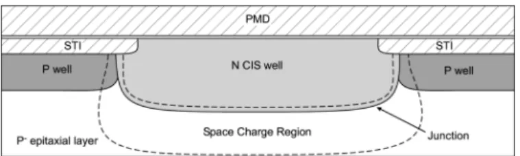
CMOS image sensor conventional photodiodes have been de- signed with typical doping profile, shape and size. The manufac- tured P-N junction perimeter is about 14 m and the area about 10 m . The contact location and the surrounding environment are similar to those used in classical CMOS sensor three-tran- sistor-active-pixels [10] (3T pixels). In order to achieve measur- able currents, 300 photodiodes have been arranged in an array and connected in parallel thanks to a first level metal intercon- nection layer. The measured dark current is therefore 300 times larger than the individual photodiode dark current. Each photo- diode is 5 m away from each others. No transistor was placed around these test photodiodes. Previous work [8] have shown that such test structures are representative of the photodiodes integrated inside CIS pixels for dark current analysis. It has also been demonstrated in this study that TID induced dark current in pixel arrays is only due to the photosensitive junction perimeter (i.e., the in pixel MOSFETs, the photodiode contact and the pho- todiode area do not play a significant role in the dark current increase after irradiation). A cross section of the studied photo- diodes is presented in Fig. 1.
In addition to these diodes, several FOXFETs have been de- signed on the same circuit to estimate the defect densities at the vicinity of the photodiode. Fig. 2 shows the FOXFET structure.
The source and the drain are made with the photodiode well, called NCIS well here, the gate is a polysilicon gate and the
Fig. 1. CIS conventional photodiode cross-sectional view.
Fig. 2. Cross-sectional view of a FOXFET with N CIS well implants used for source and drain junctions.
Fig. 3. Cross-sectional view of a photodiode with recessed STI.
gate oxide is the shallow trench isolation. It is important to no- tice that the source and the drain are completely surrounded by STI, like a classical photodiode. The drains and sources are 1.5 m long and 300 m large. The FOXFET channel width is 300 m and three lengths have been used: m, m,
and m.
Moreover, a second type of photodiode similar to the con- ventional one but with field oxide 2 m away from the diode well is available on the test chip. In this case, the depleted re- gion ends at the premetal dielectric (PMD) interface whereas it ends at the STI interface in the conventional photodiode, as illustrated in Figs. 1 and 3. The junction dimensions of this re- cessed field oxide diode (RFD) and arrangement are the same as the conventional photodiode ones. As for the conventional photodiode, dedicated FETs were realized to monitor the de- fect densities in the oxide surrounding the junction (see Fig. 4).
In this pre-metal dielectric FET (PMDFET), the gate is made with a first level metal layer on top of the PMD. The drain and the source are made with CIS photodiode implants, as for the studied FOXFETs but with recessed STI. The STI has been moved away from the channel of these PMDFETs to prevent the activation of the parasitic STI sidewall FET [8]. The channel width and length of the PMDFETs are respectively 300 m and 2 m. The drain and source junctions have the same dimensions as the FOXFET ones. All these devices were manufactured on
Fig. 4. PMDFET cross-sectional view.
the same die using a 0.18 m CMOS process dedicated to image sensors.
B. Measurement, Irradiation, and Annealing Conditions The room temperature current–voltage measurements were performed on packaged devices at 22 C and 50% relative hu- midity in a custom shielded box optimized for ultralow current measurements (leakages below 1 fA). A liquid nitrogen cryo- stat was used for temperature sweep. Ceramic packages can not be used for low level current measurements since pin-to-pin leakages can be as high as 10 pA in standard humidity and temperature conditions. In order to guaranty low leakage cur- rents, the selected packages are 16-pins TO8 metallic pack- ages on which a guard voltage can be applied. To allow the automated current-voltage characterization of several devices, a semiconductor parameter analyzer (Keithley 4200 with ded- icated preamplifiers) and a switching matrix were used. The overall test bench performance is limited by the switching ma- trix array parasitic leakage current and noise floor (between 1 and 10 fA).
TID effects in CISs operated with dynamic biases during ir- radiation and annealing can be difficult to analyze. So as a first approach, we decided to study unbiased device behaviors that can easily be compared to unbiased CIS behaviors. Moreover, unbiased FOXFET irradiation and annealing are assumed more representative of what really happens in an operated CIS since the STI surrounding the photodiode in a pixel is not biased in classical pixel designs1. As regards the photodiode, no signifi- cant difference has been observed between biased and unbiased irradiations in this technology [8], thus it is assumed that the na- ture of the degradation is qualitatively the same in both cases.
The test devices were exposed unbiased to 10 keV X-rays, at CEA-DIF, thanks to an ARACOR model 4100 semiconductor X-ray irradiator. The absorbed TID ranges from 3 krad to 1 Mrad and the dose rate was about 100 rad .
Annealing is a convenient tool for discriminating the role of gate oxide trapped charges and interface states in the degrada- tion of CMOS devices. In order to confirm the validity of this approach on the study of irradiated CISs, 30 min isochronal an- nealing steps from 35 to 300 C were realized on unbiased de- vices. At each step, the devices were placed directly on a hot metal plate which was in the oven at least 30 min before, in order to insure a quick device temperature rise. After each step, the devices were immediately put down on a cold ( C) metal plate to cool down the integrated circuit quickly.
1To estimate the effect of drain biasing during FOXFET irradiation and an- nealing will be the subject of future work.
Fig. 5. Top view illustration of a 323-3T-pixel-layout describing the photo- diode environment. The metal layers are not represented.
C. Defect Density Extraction and TCAD Simulation Details The defect densities have been extracted thanks to the McWhorter and Winokur method [11] applied to the studied FETs. In order to determine the mid-gap drain current the following equation has been used [12]:
(1) As in [13], the factor is estimated from transconduc- tance measurements. Secondary ion mass spectrometry (SIMS) was used to determine the average surface doping. Finally the trapped charge density was extracted from mid-gap voltage shift and the interface state density from the subthreshold slope. The defect densities presented in the paper after each irradiation and annealing step come from an average of the densities ex- tracted on all the thick oxide FETs (four FOXFETs with
, two with , two with
and two PMDFETs with per step).
Qualitative technology computer-aided design (TCAD) sim- ulations were realized by using SENTAURUS tools to validate the interpretations. The vertical doping profiles used in these simulations were estimated by SIMS and the lateral doping profiles were roughly extrapolated from the vertical measured profiles.
III. RADIATIONINDUCEDDARKCURRENTANALYSIS
A. Nature of Dark Current
In a classical 3T-active-pixel, the photodiode is surrounded by a field oxide, as illustrated in Fig. 5. A cross-ectional view along the x-axis would lead to a drawing similar to Fig. 2, but
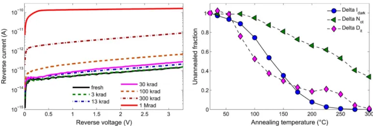
Fig. 6. CIS conventional photodiode reverse current–voltage characteristics evolution with irradiation (300 photodiodes in parallel).
without the polysilicon gate on top. It means that a CIS photo- diode can be seen as the drain junction of a FET in which the field oxide play the role of the gate oxide. Thus, all the sources of drain leakage current usually observed in MOSFETs (see [14], for example) can be considered as a possible source of radiation induced dark current:
• drain junction diffusion current (from N and P neutral regions);
• drain junction Shockley-Read-Hall (SRH) generation cur- rent from the depleted region (with or without electric field enhancement);
• tunneling currents (band-to-band, trap assisted);
• subthreshold weak inversion conduction;
• gate-induced-drain-leakage (GIDL);
• gate leakage current;
• and drain to source punchthrough current.
Because of the relatively large thickness of the STI oxide, gate leakage current can be neglected. In a standard CIS which does not use high resistivity substrate or high voltage (larger than op- erating voltages), photodiode depleted regions are not supposed to merge in the bulk and TID defects have no reason to change significantly the depleted region far from the surface. Hence, punchthrough effect will not be considered in the following.
The current–voltage measurements performed on 300 CIS photodiodes in parallel are presented in Fig. 6. The photodiode reverse current, also called dark current, increases monoto- nously with TID and reverse voltage up to 300 krad. According to ideal PN junction theory [12], the continuous increase with reverse voltage suggests that the radiation induced dark current is dominated by SRH generation without field enhancement [15]. Indeed, an electric field enhancement would lead to a soft breakdown [16] visible on suchI–Vcharacteristics and diffu- sion dominated dark current would not increase with reverse voltage after a few kT. As regards tunneling contributions, they would also induce a much larger dark current rise with reverse bias [17], [18]. Absence of tunneling is not surprising considering the relatively low doping concentrations used in the photodiode structure.
Fig. 7. FOXFET subthreshold characteristics evolution with irradiation. The presented curve comes from a FOXFET withW = 300 m andL = 0:7 m.
The applied drain to source voltage was 3.3 V.
Fig. 7 presents the measurements performed on one 300 m/0.7 m FOXFET with drain to source voltage fixed to 3.3 V. The drain leakage current when the gate voltage is around zero corresponds to the dark current of the CIS photodiode2. One can see that this current also rises with TID and that gate voltage does not have any influence on it up to 100 krad of TID. This agrees with the previous conclusion (i.e., that SRH generation process is the most probable source of TID induced dark current) and also shows that GIDL and subthreshold con- duction current do not contribute to the drain leakage current, and so to the CIS photodiode dark current up to 100 krad.
Above 100 krad, the subthreshold conduction current starts to dominate the drain leakage current measured for zero gate voltage. This effect is still not visible on the photodiode I–V characteristics (Fig. 6) after 300 krad because the W/L ratio of the studied FOXFET represents a worst case in comparison to the real parasitic FOXFET surrounding the photodiodes in the array. At 1 Mrad, the photodiode dark current becomes independent of the reverse voltage. This could be explained by the prevalence of the weak inversion current, which does not depend on drain voltage for drain voltage greater than a few kT [12], but it is not likely since all the test photodiodes in the array are biased at the same potential. This independence on reverse voltage could also be explained by a merge between the test photodiode depleted regions at the STI interface. In this case, the depleted region would not extend at the surface anymore but would extend in the bulk for increasing reverse bias leading to an apparent constant current with reverse bias. It must be emphasized that once the depleted region have merged at the STI interface, weak inversion current can become significant if adjacent photodiodes are biased at different potentials, which usually happen in operated CISs.
Recent work [8] has shown that the radiation induced dark current is directly proportional to the photodiode perimeter
2The TID induced dark current proportionality with the photodiode perimeter was observed [8] from very small photodiodes (i.e., as small as the one tested here) to photodiodes as long as 4000m. The drain leakage current linear den- sity (dark current divided by the junction perimeter) of the studied FOXFETs is then believed to be comparable to the studied photodiode dark current linear density despite the difference in size.
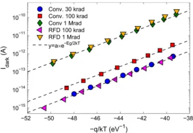
Fig. 8. Photodiode dark current Arrhenius plots for several TID (300 photodi- odes in parallel). The data are compared to exponential functions proportional toexp 0E =2kT. During measurement, the photodiodes were reverse biased to 3.3 V.
in this technology3. It was then concluded that the generation current was coming from the peripheral depleted STI interface.
Considering a uniform interface state energy distribution equals to throughout the bandgap, the worst case4SRH generation dark current can be expressed as [20]
(2) where is the reverse voltage, is the depleted region thickness at the STI interface, is the junction perimeter, is the effective capture cross section of the STI interface centers equals to . If the temperature dependence of and are neglected in front of the exponential term, the tempera- ture dependence of this STI interface generation current can be expressed
(3) The measured dark current temperature dependence of con- ventional and RFD photodiodes are presented in Fig. 8. It can clearly be seen that whatever the TID, the extracted activation energy corresponds pretty well to , even after 1 Mrad.
This confirms that the main contribution to TID induced dark current is an interface state SRH generation current, even after 1 Mrad when the depleted regions have merged.
The same conclusions can be drawn about the recessed field oxide diode and PMDFET characteristics presented in Figs. 8, 9, and 10. Therefore, in the following, the dark current in the conventional and RFD photodiodes will be assumed to be cor- rectly described by (2).
B. Role of Interface States and Trapped Charges
A straightforward way to discriminate the role of interface states and trapped charges in a irradiated CISs, is to perform an
3Similar behaviors have been reported in older CMOS technologies [4], [6].
4The generation rate is assumed constant throughout the depleted region and equals to its maximum value leading to an overestimation of the total generation current value [19].
Fig. 9. Recessed STI photodiode reverse current-voltage characteristics evolu- tion with irradiation (300 photodiodes in parallel).
Fig. 10. PMDFET subthreshold characteristics evolution with irradiation. The transistor aspect ratio isW = 300 m andL = 2 m and the applied drain to source voltage was 3.3 V.
isothermal or isochronal accelerated annealing and to compare the dark current evolution to the known annealing behavior of radiation induced defects in thermally grown thin gate oxides. It is well established that in most of the cases, a temperature of 100 C is sufficient to accelerate consequently the trapped charge annealing rate in MOSFET gate oxide whereas it is not supposed to be high enough to change significantly the annealing rate of interface states [21]. Furthermore, rise of interface state density have been frequently reported after a 100 C annealing [22].
Fig. 11 presents the result of the grounded isochronal an- nealing performed on the conventional photodiode and the as- sociated FOXFETs. The defect densities were extracted by the method described in Section II-C. The annealed devices were exposed to 300 krad. One can see that the radiation induced dark current decreases continuously with increasing annealing tem- perature. In contrary to what can be expected from MOSFET gate oxide behavior, radiation induced interface states anneal out quickly after 75 C and disappear almost completely after 300 C. As regards the trapped charge, 30% of the radiation in- duced charge remains after the 300 C. Similar thick oxide be- haviors were observed in the same technology after biased and
Fig. 11. Radiation induced photodiode dark current, trapped charge density and interface state density evolution during the isochronal annealing experiment (30 min isochronal annealing step duration).
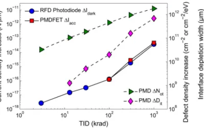
Fig. 12. Conventional photodiode dark current (V = 3:3V) and FOXFET accumulation mode current (withV = 3:3V) increases compared to trapped charge and interface state density increases with total dose.
unbiased 100 C isothermal annealing [8], and in standard DSM CMOS processes after biased isochronal annealing [9]. All these observations lead to the conclusion that performing annealing on irradiated CISs without estimating the defect densities will not help discriminating the role of trapped charges and interface states in the degradation.
In order to clarify the role of interface states and trapped charges in the TID induced dark current increase, the evolution of defect concentrations with total dose have been compared to the dark current variations. The average defect density increases measured on all the studied FOXFETs are compared to the dark current rise and the FOXFET accumulation regime drain reverse current increase in Figs. 12 and 13. This accumulation mode current is defined here as the drain current measured when the gate voltage is below the mid-gap voltage, i.e., the constant drain leakage value observed for small or negative gate bias. When divided by the junction perimeter, the FOXFET accumulation mode current density and the photodiode dark current density are nearly the same. This confirms that the radiation induced dark current mainly comes from the junction perimeter where the depleted region reaches the STI (as concluded in [8]).
Fig. 13. Recessed STI photodiode dark current (V = 3:3V) and PMDFET accumulation mode current (withV = 3:3V) increases compared to trapped charge and interface state density increases with total dose. For1D values below10 cm 1 eV , the differences in subthreshold slope was below the measurement uncertainty, therefore these1D values are not reliable.
Fig. 14. Conventional photodiode dark current density increase compared to interface state density increase with TID.
As a first approach, the effects of the trapped charge on the radiation induced dark current can be neglected, and from (2) one can write
(4) Therefore, the dark current increase should be directly proportional to the interface state density increase . Fig. 14 clearly shows that the relationship between and is not linear (i.e., does not follow the plot). A similar nonlinear evolution was observed on the RFD diode. Hence, (4) is not a valid description of the observed degradation and the contribution of trapped charges must be taken into account.
The radiation induced trapped charge changes the elec- trostatic equilibrium at the surface. This charge should have an impact on the depleted region extension at the periphery of the photodiode, like the biased gate of a gated photodiode [20].
Thus, the dependence of (2) with TID can be expressed as
(5)
Fig. 15. Evolution ofW with trapped charge density in the conventional CIS photodiode. The experimental data are plotted by using (6) and taking D = 1:4 2 10 cm 1 eV and = 2 2 10 cm .
Fig. 16. Evolution ofW with trapped charge density in the recessed STI photodiode. The experimental data are plotted by using (6) and takingD = 2:3 2 10 cm 1 eV and = 1:26 2 10 cm .
There are three unknowns in (5): the depletion region extension at the STI interface , which varies with the TID, the interface state density before irradiation and the effec- tive capture cross section . In order to appreciate the evolu- tion of with TID, and roughly estimate the other unknowns, the following function is plotted in Fig. 15:
(6) The value has been chosen by assuming that
is close to . In other words, at low TID, the effect of the induced trapped charge on the dark current in- crease is considered to be small. As regards , its value has been selected to insure that matches the de- pleted width computed with TCAD simulations. It is important to notice that the uncertainty on has almost no effect on the plotted function at high TID (when ) whereas does not change the shape of the curve but only changes the absolute values.
The result of this analysis applied to both types of photodiode is presented in Figs. 15 and 16. The order of magnitude of the se- lected values corresponds to what is usually reported [21].
Fig. 17. Overview of the TCAD simulation (with no trapped charge). The sim- ulation of two half-conventional photodiodes with 5m of STI between them is presented.
Fig. 18. Conventional photodiode TCAD simulation with no trapped charge.
The area of interest has been magnified to clearly show the space charge region extension along the STI/Si interface.
Fig. 19. Conventional photodiode TCAD simulation with a trapped charge density of1:5 2 10 cm ( 7krad).
As regards the achieved values, interface state density is expected to be lower than cm in state of the art deep-submicrometer MOSFET gate oxide, so it does not seem unrealistic to find values around cm at the STI in- terface. Furthermore, all the ideal hypothesis used to obtain (6) can easily justify more than a factor of two between measured and theoretical values.
These figures show that up to a trapped charge density of cm (about 6 krad for the tested FOXFETs), the interface de- pletion width only slightly changes (less than 10% variation).
However, between and cm (between 6 and 300 krad for the tested FOXFETs), the trapped charge has a large impact on the depleted region, leading to a large enhancement
Fig. 20. Conventional photodiode TCAD simulation with a trapped charge density of3:2 2 10 cm ( 25krad).
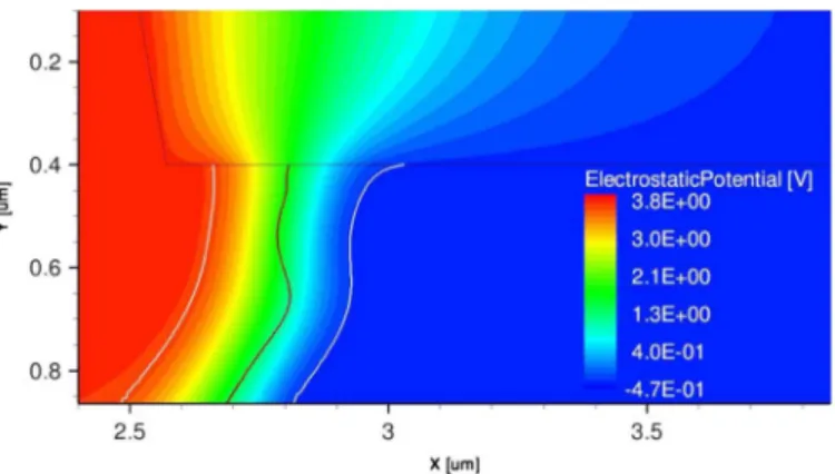
Fig. 21. Conventional photodiode TCAD simulation with a trapped charge density of1 2 10 cm ( 160krad).
of the dark current. In the experiments and simulations reported here the depleted region extension saturates when two adjacent photodiode depletion region merge (i.e., 2.5 m for the con- ventional photodiode and 2 m for the RFD diode). This effect would appear at lower TID for usual pixel layout where adjacent photodiodes are much closer to each others.
TCAD simulations showing the impact of trapped charge in the thick oxide on the depleted region extension at the STI inter- face are presented in Figs. 17 –21. Fig. 17 presents an overview of two adjacent test photodiodes before irradiation and shows the complete simulated structure. As discussed from experi- mental data, up to cm only a slight change of the total depleted width at the interface can be seen (see Figs. 18 and 19). However, one can notice the slight reduction of depletion width in the N doped region which is compensated by a small extension in the P region. At higher trapped charge densities, the space charge region extends rapidly in the P type region (see Fig. 20) until the two depleted region merge as shown in Fig. 21.
It is interesting to notice that by transposing the voltage-doping transformation concept [23] from short channel MOSFET ef- fects to our problem, the observed influence of a trapped charge increase on depletion width can be explained by a reduction of the effective P doping concentration (and a rise of the effective N doping concentration) at the STI interface. In this case, the effective doping value is directly connected to the electric field induced by the trapped charge.
The simulated depletion width at the oxide interface is com- pared to the experimental data in Figs. 15 and 16. One can see that the simulated effect corresponds qualitatively to the measured effect, validating the deduced role of trapped charge
in dark current enhancement. However, the trapped charge at which the depletion regions merge is roughly three times lower in the simulation than in the experimental data. These discrep- ancies are acceptable if we keep in mind all the simplifying hy- pothesis used, the defect density estimation uncertainty and the rough evaluation of doping profile from SIMS measurements.
IV. SUMMARY ANDCONCLUSION
The TID induced dark current rises of two types of CIS pho- todiodes were analyzed and compared to interface state and trapped charge density increases from 3 krad to 1 Mrad. First, we showed that the radiation induced dark current was due to SRH generation process, without field enhancement. The in- terface state density rise with TID was not sufficient to justify the observed degradations. Thanks to a simple analytical de- velopment confirmed by TCAD simulation, it was shown that between about 6 and 300 krad the radiation induced trapped charge extends the space charge region at the oxide interface, leading to an enhancement of the generation current due to in- terface states. Beyond 300 krad, the depleted regions of adja- cent photodiode merge and inter device leakage was observed in the FOXFETs where the drain to source voltage was larger than zero. One should notice that the demonstrated role of in- terface states and trapped charges in dark current increase can be transposed to any CIS photodiode (and pixel) as long as the space charge region reaches an oxide interface. Isochronal an- nealing was also performed and interface states annealed out at temperature lower than 100 C whereas about a third of the trapped charge remained after 30 minutes at 300 C.
These observations can have several consequences on pho- todiode hardening-by-design techniques. It is clear that two ef- fects have to be mitigated in order to improve the radiation hard- ness: the generation center density increase and the depleted re- gion extension with TID (to reduce the dark current increase and also to prevent inter device leakage). The first point is dif- ficult to mitigate by design, except by trying to surround the photodiode with an oxide which have a slower interface state buildup than STIs (gate oxide for example). The space charge region extension can potentially be controlled in several ways, like using well chosen and well placed P implants, or by con- trolling the surface potential thanks to a polysilicon gate (as in [4]). Several test structures are being tested to verify these con- clusions. It is worth mentioning that the most straightforward way to reduce the radiation induced dark current in CIS pho- todiodes, is to reduce the junction perimeter (which will have an impact on quantum efficiency and charge to voltage conver- sion factor). As regards accelerated annealing and qualification tests of CISs, it should be emphasized that the major degrada- tion of modern CISs is due to interface state buildup and charge trapping in STIs. Hence, STI behavior after irradiation and an- nealing has to be well understood before allowing the complete understanding of CIS behavior under ionizing radiation.
ACKNOWLEDGMENT
The authors are grateful to M. Gaillardin and C. Marcandella from CEA DAM DIF for taking care of irradiations. The au- thors also thank C. Duprat (from INSA-AIME), P. Pinel and F. Corbière (from ISAE) for their help with circuit design, pack- aging, and experimental issues.
REFERENCES
[1] G. R. Hopkinson, “Radiation effects in a CMOS active pixel sensor,”
IEEE Trans. Nucl. Sci., vol. 47, no. 6, pp. 2480–2484, Dec. 2000.
[2] M. Cohen and J.-P. David, “Radiation-induced dark current in CMOS active pixel sensors,” IEEE Trans. Nucl. Sci., vol. 47, no. 6, pp.
2485–2491, Dec. 2000.
[3] E.-S. Eid, T. Y. Chan, E. R. Fossum, R. H. Tsai, R. Spagnuolo, J. Deily, W. B. Byers, and J. C. Peden, “Design and characterization of ionizing radiation-tolerant CMOS APS image sensors up to 30 Mrd (Si) total dose,”IEEE Trans. Nucl. Sci., vol. 48, no. 6, pp. 1796–1806, Dec. 2001.
[4] B. R. Hancock, T. J. Cunningham, K. P. McCarty, G. Yang, C. J.
Wrigley, P. G. Ringold, R. C. Stirbl, and B. Pain, “Multi-megarad (Si) radiation-tolerant integrated CMOS imager,” inProc. SPIE, 2001, vol.
4306, pp. 147–155.
[5] J. Bogaerts, B. Dierickx, G. Meynants, and D. Uwaerts, “Total dose and displacement damage effects in a radiation-hardened CMOS APS,”
IEEE Trans. Electron Devices, vol. 50, no. 1, pp. 84–90, Jan. 2003.
[6] B. Pain, B. R. Hancock, T. J. Cunningham, S. Seshadri, C. Sun, P.
Pedadda, C. J. Wrigley, and R. C. Stirbl, “Hardening CMOS imagers:
Radhard-by-design or radhard-by-foundry,” inProc. SPIE, 2004, vol.
5167, pp. 101–110.
[7] M. Beaumel, D. Hervé, and D. Van Aken, “Cobalt-60, proton and elec- tron irradiation of a radiation-hardened active pixel sensor,” Radiation and its Effects on Components and Systems. Bruges, Belgium, Sep.
14–18, 2009.
[8] V. Goiffon, P. Magnan, O. Saint-Pé, F. Bernard, and G. Rolland,
“Total dose evaluation of deep submicron CMOS imaging technology through elementary device and pixel array behavior analysis,”IEEE Trans. Nucl. Sci., vol. 55, no. 6, pp. 3494–3501, Dec. 2008.
[9] F. Faccio, H. J. Barnaby, X. J. Chen, D. M. Fleetwood, L. Gonella, M. McLain, and R. D. Schrimpf, “Total ionizing dose effects in shallow trench isolation oxides,”Microelectron. Rel., vol. 48, no. 7, pp. 1000–1007, Jul. 2008.
[10] E. R. Fossum, “CMOS image sensors: Electronic camera-on-a-chip,”
IEEE Trans. Electron Devices, vol. 44, no. 10, pp. 1689–1698, Oct.
1997.
[11] P. J. McWhorter and P. S. Winokur, “Simple technique for separating the effects of interface traps and trapped-oxide charge in metal-oxide- semiconductor transistors,”Appl. Phys. Lett., vol. 48, pp. 133–135, Jan.
1986.
[12] S. M. Sze, Physics of Semiconductor Devices, 2nd ed. New York:
Wiley, 1981.
[13] R. Pease, D. Emily, and H. E. Boesch, Jr., “Total dose induced hole trapping and interface state generation in bipolar recessed field oxides,”
IEEE Trans. Nucl. Sci., vol. 32, pp. 3946–3952, 1985.
[14] K. Roy, S. Mukhopadhyay, and H. Mahmoodi-Meimand, “Leakage current mechanisms and leakage reduction techniques in deep-submi- crometer CMOS circuits,”Proc. IEEE, vol. 91, no. 2, pp. 305–327, 2003.
[15] G. Vincent, A. Chantre, and D. Bois, “Electric field effect on the thermal emission of traps in semiconductor junctions,”J. Appl. Phys., vol. 50, no. 8, pp. 5484–5487, 1979.
[16] M. J. J. Theunissen, “Analysis of the soft reverse characteristics ofn p drain diodes,”Solid-State Electron., vol. 28, pp. 417–425, 1985.
[17] G. A. M. Hurkx, H. C. De Graaff, W. J. Kloosterman, and M. P.
G. Knuvers, “A new analytical diode model including tunneling and avalanche breakdown,”IEEE Trans. Electron Devices, vol. 39, no. 9, pp. 2090–2098, 1992.
[18] N. V. Loukianova, H. O. Folkerts, J. P. V. Maas, D. W. E. Verbugt, A.
J. Mierop, W. Hoekstra, E. Roks, and A. J. P. Theuwissen, “Leakage current modeling of test structures for characterization of dark current in CMOS image sensors,”IEEE Trans. Electron Devices, vol. 50, no.
1, pp. 77–83, 2003.
[19] M. Shur, Physics of Semiconductor Devices. Englewood Cliffs, NJ:
Prentice-Hall, 1991.
[20] A. S. Grove and D. J. Fitzgerald, “Surface effects on p-n junctions:
Characteristics of surface space-charge regions under non-equilibrium conditions,”Solid-State Electron, vol. 9, no. 8, pp. 783–806, 1966.
[21] T. P. Ma and P. V. Dressendorfer, Ionizing Radiation Effects in MOS Devices and Circuits. New York: Wiley-Interscience, 1989.
[22] J. Schwank, D. Fleetwood, M. Shaneyfelt, P. Winokur, C. Axness, and L. Riewe, “Latent interface-trap buildup and its implications for hard- ness assurance,”IEEE Trans. Nucl. Sci., vol. 39, no. 6, pp. 1953–1963, 1992.
[23] T. Skotnicki, G. Merckel, and T. Pedron, “The voltage-doping trans- formation: A new approach to the modeling of MOSFET short-channel effect,”IEEE Electron Device Lett., vol. 9, no. 3, pp. 109–112, 1988.