A
4th
Order Continuous-Time AE ADC with
VCO-Based Integrator and
Quantizer
MASSACUSETTS INSTITUTEOF TECHN-OLOGY
by
MAR 0 5 2009
Matthew Jeremiah Park
Li BRARIES
B.S. in Electrical Engineering and Computer Science
Massachusetts Institute of Technology, 2004
M.Eng. in Electrical Engineering and Computer Science
Massachusetts Institute of Technology, 2005
Submitted to the Department of Electrical Engineering and Computer
Science
in partial fulfillment of the requirements for the degree of
Doctor of Philosophy
at the
MASSACHUSETTS INSTITUTE OF TECHNOLOGY
February 2009
@
Massachusetts Institute of Technology 2009. All rights reserved.
Author
...
Department of Electrical Engineering and Computer Science
February, 2009
Certified by
...
Michael H. Perrott
Visiting Associate Professor
,
,
Thesis Supervisor
Accepted by
...
Terry P. Orlando
Chairman, Department Committee on Graduate Students
A
4th Order Continuous-Time AE ADC with VCO-Based
Integrator and Quantizer
by
Matthew Jeremiah Park
Submitted to the Department of Electrical Engineering and Computer Science on February, 2009, in partial fulfillment of the
requirements for the degree of Doctor of Philosophy
Abstract
The use of a VCO-based integrator and quantizer within a continuous-time (CT) AE analog-to-digital converter (ADC) structure is explored, and a custom prototype in a 0.13 pm CMOS with a measured performance of 81.2/78.1 dB SNR/SNDR over a 20 MHz bandwidth while consuming 87 mW from a 1.5V supply and occupying an active area of 0.45 mm2 demonstrated. A key innovation is the explicit use of the oscillator's output phase to avoid the signal distortion that had severely limited the performance of earlier VCO-based ADC's, which exclusively made use of the output frequency. Furthermore, the proposed architecture includes a scheme for performing fast dynamic element matching (DEM), enabling first-order shaping of unit-element mismatch in all feedback DAC's.
Thesis Supervisor: Michael H. Perrott Title: Visiting Associate Professor
Acknowledgments
But he said to me, 'My grace is sufficient for you, for power is made perfect in weakness.' So, I will boast all the more gladly of my weaknesses, so that the power of Christ may dwell in me.
2 Corinthians 12:9 NRSV
It is extremely difficult for me to describe my feelings about (finally) leaving MIT. This campus has been my home for more than 8 years, longer than I have ever lived in a single location in my lifetime. I've traversed its labyrinthine corridors at obscene hours, spent innumerable days and nights studying for exams and working on problem sets in its cavernous libraries and secluded reading rooms, and toiled in its soulless laboratories for many restless days and harrowing nights. To be honest, I'm amazed that I was able to endure it all with my sanity (relatively) intact.
But my experience at MIT was so much more than blood, sweat and tears. It was an honor to be here, especially because of the phenomenal people that I had the privilege to work with and meet. I owe my utmost thanks and gratitude to my advisor and friend, Mike Perrott, whom I have had the gift of knowing since my sophomore year. Mike has been not only a fantastic and patient teacher (from 6.003 recitations to advanced mixed-signal design), but also a dedicated mentor, an honest assessor of my work, and a committed advocate of my research. Mike's exemplary humility, integrity, and grace established a similar culture and spirit within the High Speed Circuits and Systems Group. Looking back, I marvel at how well the group worked together and supported each other, with its members volunteering their time and effort to help each other make a tapeout deadline. My association with this group is something that I am so proud of and will cherish forever.
I owe special thanks to two of the Perrott Group's earliest students, Ethan Crain and Scott Meninger. Ethan bravely accepted his role as my mentor when I first joined the group as a clueless M.Eng. student. He taught me the basics of chip design, simulation, and layout--all while raising three children, taping out, TA'ing a
class, preparing a talk for ISSCC, and writing a thesis and journal paper. Scott was another great mentor and confidant; his willingness to brainstorm ideas and review my designs helped me improve as a designer as well gain confidence in my abilities. At the same time, his thoroughness in his work was an amazing example that I still strive to replicate.
Matt Straayer and Kerwin Johnson also deserve special recognition for all the help they have given me over the years. Matt's early efforts in VCO-based ADC design laid a lot of the groundwork for my thesis project, and played a crucial role in making it a success. His deep and very intuitive grasp of circuit design helped me test out new ideas and explore different architectures, and his sheer efficiency and productivity when working were both a great inspiration and motivation. Kerwin was the Perrott group's CAD, Cadence and wirebonding wizard par excellence, and designed the pads and padframe for the entire IBM tapeout team. He generously and selflessly shared his encyclopedic knowledge about almost every conceivable topic with me on countless occasions, an experience that was not only enriching but also lots of fun!
The results presented in this thesis would also not be possible without the generous help of Charlotte Lau and Min Park. Charlotte assisted me during the tapeout crunch by laying out the high speed output buffers. She was also a calming voice of strength and support during all those days and nights when we were feverishly working to finish the tapeout on time. Min Park (along with Kerwin Johnson) graciously offered his deft fingers to wirebond a few of my chips on several of my trips to the Harvard labs. At the same time, his interminable optimism and fighting spirit toward research boosted my spirits on many occasions when I felt burnt out from work.
Chun-Ming Hsu and Belal Helal were an indispensable aid throughout the tapeout and testing process. Given the similarity of my project to a PLL, Chun-Ming offered a unique perspective on my work, and gave useful feedback on many of my crazy ideas. At the same time, he was great listener and an assuring presence whenever I talked to him about my thoughts and concerns about future careers and pursuits. Belal (along with Min Park) designed the serial interface used by almost all the chips in the IBM tapeout, and frequently demonstrated his sincere desire to expedite the
group's work by investigating and applying useful software and hardware tools. I know that my PCB-designing and chip testing experiences were that much easier to accomplish thanks to the detailed instructions and tutorials he wrote for the benefit of the entire group.
Professors Joel Dawson and Vladimir Stojanovic sat on my committee from the day I proposed my thesis, and have been such an awesome support throughout the entire process. In preparing this thesis, Joel encouraged me to emphasize the big picture behind this work, which helped me present the project in a manner that will excite and intrigue the unfamiliar reader. Vladimir helped me get access to the high speed pattern generator that I desperately needed during testing, and graciously offered his assistance with acquiring any other lab equipment that I might need.
I am indebted to our group secretary, Valerie DiNardo, for all the time and effort she put in on my behalf to navigate MIT's incredibly complicated accounting and treasury departments. Without her vast knowledge, I would not have been able to obtain crucial purchase orders and reimbursements, and would have had to fight unruly vendors on my own.
Two people who are unrelated to this thesis project, but nevertheless played a very important role in my graduate career are John Bulzacchelli and Jungwon Kim. John was my mentor during my internship at IBM research, and was an incredible teacher and friend. His passion and dedication for engineering and research were truly an inspiration for me, and his selfless devotion to my project and my education is something that I will always remember with profound gratitude. Jungwon was my partner in my master's project, and together we traveled the long road (4 years, phew!) to demonstrating a working optical-electrical 40 GHz sub-sampling receiver and ADC. He is an optics guru extraordinaire, an incredibly talented scientist and engineer, and an all-around awesome person who will undoubtedly become a giant in his field.
Sungah Lee deserves very special words of acknowledgement and thanks. She was a constant companion, supporter and friend, and faithfully stayed at my side during the bulk of my Ph.D. When times were tough, she was always there to give me a
warm hug and to offer encouraging words. Without her comforting presence, this Ph.D. probably would not have been possible, and I am extremely grateful to her for all the loving care and support she gave me.
It almost goes without saying that my family has been a source of unflagging support and guidance for me during my many years at MIT. I know my parents and my grandmother have been praying for me everyday throughout my life, and the very fact that I am where I am at this moment in my life is largely a reflection of their constant and fervent requests on my behalf for God's blessing, protection and guidance. My mother, father and grandmother have also been my role models, and their examples of love, humility, integrity, leadership and professionalism have always served as a guiding light to me throughout my education. My sister Cathy and my brother-in-law George have been my cheerleaders for as long as I can remember, and always believed in my abilities whenever I was in doubt. At the same time, they generously cared for and lavished me with me so many gifts, yet never asked for anything in return other than my well being and happiness. I can't express how indebted I am to their tremendous loving support. My love and gratitude to everyone in my family is so enormous that it is ineffable; I only hope that I can make them proud in everything that I do.
I chose the passage from 2 Corinthians because of something very similar that my father told me when I was going through an extremely difficult time in graduate school: "In all things, God's grace is sufficient." This thesis, my graduate training, my education at MIT, and every blessing and hardship I've experienced in life are due to God's infinite grace and love. Through all times, good and bad, God never abandoned me but used the circumstances to make me stronger and shape me into the person I am today. If MIT has taught me anything, it is that I always need to have faith in His plan for my life.
Biography
Matt Park, American, b. 1981
A Portrait of the Artist as a Young Man 2000-2008
Oil on canvas
Museum of Questionable Art, Cambridge: Park Collection
Matthew Jeremiah Park was born in Rochester, New York, on September 4, 1981. He attended Masuk High School in Monroe, Connecticut from 1996 to 1998, and then Northern Valley Regional High School in Old Tappan, New Jersey from 1998 to 2000. He entered the Massaschusetts Institute of Technology (M.I.T.) in September 2000. As a member of M.I.T.'s VI-A co-op program, he was an internship student at M.I.T. Lincoln Laboratories, Lexington, Massachusetts in the summer of 2002, and at Linear Technology, New Chelmsford, Massachusetts in the summer of 2003. In January 2004, he began an undergraduate research study (UROP) in the M.I.T. Microsystems Technology Laboratory as part of the High Speed Circuit and Systems (HSCS) Group under the supervision of Professor Michael Perrott. During this time, he worked on a circuit implemention of the Dynamic Weighted Averaging (DWA) algorithm for use in a high bandwidth fractional-N frequency synthesizer. He received the B.S. degree from the Department of Electrical Engineering and Computer Science (EECS) at M.I.T. in June 2004.
From September 2004 until May 2005, he was a Research Assistant in the HSCS Group. His research in new opto-electronic receiver and analog-to-digital converter (ADC) architectures formed the basis of his M.Eng. thesis entitled An Optical
He received the M.Eng. degree in EECS in June 2005.
From June 2005 until August 2005, he was a Graduate Research Scientist at the IBM T.J. Watson Research Center, Yorktown Heights, New York, where he investi-gated low-power decision-feedback equalizer (DFE) architectures leveraging current integration. He returned to the HSCS Group in September 2005 to begin his doctoral research on high-resolution VCO-based ADC's. He successfully defended his
disser-tation entitled A 4th Order Continuous-Time AE ADC wzth VCO-Based Integrator
and Quantizer in November 2008, and received his Ph.D. degree in EECS in February
2009. His present research interests include mixed-signal circuit and systems design and opto-electronic systems.
Contents
1 Introduction 23
1.1 A Brief Overview of CT AE ADC's ... 23
1.2 Motivations for Investigating VCO-Based ADC's . ... 30
1.3 Benefits of a VCO-based ADC architecture . ... 31
1.4 Prior VCO-Based ADC Architectures ... 33
1.5 Proposed Continuous-Time AE ADC Architecture . ... 39
1.5.1 Voltage-to-phase quantization . ... 39
1.5.2 Proposed 4th-order CT AE Loop Filter . ... . 43
1.5.3 First-order dynamic weighted averaging (DWA) sequence gen-eration ... ... 46
1.6 Thesis Outline ... ... 51
2 Behavioral Simulation 53 2.1 Amplifier Finite Gain-Bandwidth ... . 55
2.2 Amplifier Non-Linearity ... ... 61
2.3 Finite DAC Impedance ... ... 63
2.4 Device Noise ... ... ... 69
2.5 VCO Unit Element Mismatch ... ... 69
2.6 Main NRZ DAC Unit Element Mismatch . ... 71
2.7 Main NRZ DAC Inter-Symbol Interference (ISI) . ... 74
2.8 Minor-Loop NRZ and RZ DAC Unit-Element Mismatch and ISI . . . 78
2.9 Clock Jitter . ... ... . . . . 78
3 Circuit Design
3.1 Analog Core . . ...
3.1.1 Loop Filter Passives and Calibration 3.1.2 Opamp Design ...
3.1.3 Main and Minor-Loop NRZ Feedback
3.1.4 RZ feedback DAC . ...
3.1.5 VCO Integrator and Quantizer . . .
3.2 Digital Core . . ...
3.2.1 DWA Barrel Shift and Accumulator .
3.2.2 Clocking ... 3.2.3 Output Buffers ... 83 .. . . . 83 . . . . . . . . . 84 ... . . . . . 84 DAC's . ... 88 .. . . . 94 .. . . . . . 95 .. . . . 98 . . . . . . . . . . 99 . . . ... . . . . .. 101 . ... 103 4 Measured Results 5 Future Directions 5.1 Architectural Improvements . ...
5.1.1 A Lower ISI DAC Topology . . . .
5.1.2 Going Beyond a 4-bit Quantizer/DAC
5.1.3 A Faster DWA Implementation . . .. 5.2 Scaling of the Proposed Architecture in Future
5.2.1 Impact of Scaling on Opamp Design .
5.2.2 Impact of Scaling on DAC Design . . .
105 111 112 112 120 121 124 124 131 133 Technology Nodes 6 Conclusion
List of Figures
1-1 survey of the resolution and bandwidth of popular ADC topologies
presented at ISSCC and VLSI from 1997-2008 [38]. . ... 24
1-2 (a) inherent anti-alias filtering due to location of sampler after loop filter in a CT AE ADC, and (b) risk of aliasing due to sampling of
input-signal without any filtering in a DT AE ADC. . ... 25
1-3 prototypical receiver architectures assuming (a) an arbitrary DT ADC preceded by an explicit anti-alias filter (b) a CT AE ADC providing inherent anti-alias filtering, and (c) a bandpass CT AE ADC that elim-inates the IF mixer, performs anti-alias filtering at the IF frequency, and downcoverters the IF signal in the digital domain using a DSP. 27 1-4 clock jitter appearing at ADC input due to modulation of charge in a
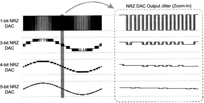
1-bit NRZ and RZ feedback DAC. ... . 28
1-5 reducing the amount of charge modulation by clock jitter by increasing
the number of bits in a multibit NRZ DAC. . ... 29
1-6 the VCO voltage-to-frequency and voltage-to-phase relationships. . . 31
1-7 multibit quantization with a ring oscillator structure. . ... 33
1-8 multibit quantization using a conventional voltage flash architecture. 34 1-9 (a) single-phase and (b) multiple-phase counting ADC architectures.. 35 1-10 a multi-phase VCO ADC that eliminates the counter by oversampling
the VCO phase. ... ... ... 36
1-11 analytical model of the voltage-to-frequency VCO ADC, and the
equiv-alent frequency domain block diagram. ... 37
1-12 VCO-based ADC that achieved third-order shaping with feedback and
an additional passive and active integrator [55]. . ... . 39
1-13 (a) prior voltage-to-frequency VCO-based ADC architecture that suf-fered from distortion due to K, non-linearity, and (b) proposed voltage-to-phase VCO-based ADC that is immune to distortion caused by Kv
non-linearity. . ... ... 40
1-14 FFT's generated from the behavioral simulation of the 5-bit (31-stage) VCO-based quantizer assuming (a) the prior voltage-to-frequency and (b) the proposed voltage-to-phase architectures. SNDR is calculated over a 20 MHz bandwidth, a -1 dBFS input signal, and a sample rate
of 1 GHz. ... ... ... 42
1-15 loop delay compensation using a second feedback DAC (DACB) around the quantizer to generate the desired filter impulse response [64]. . . . 44 1-16 loop delay compensation by differentiating the quantizer output and
then integrating the resulting DAC signal. . ... 44
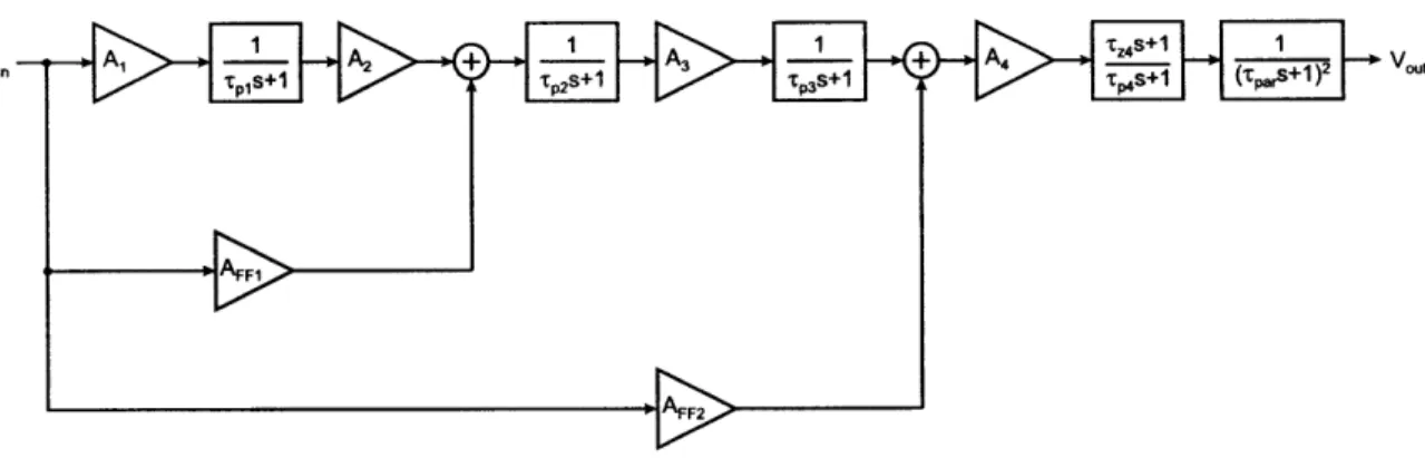
1-17 loop filter block diagram with VCO quantizer and feedback DAC's
indicated. ... ... ... 45
1-18 Bode plot of the (a) loop filter and (b) noise-transfer function (NTF)
assuming a clock frequency of 900 MHz (OSR=22.5). . ... 47
1-19 schematic of the proposed 4th-order CT AE ADC with VCO quantizer. 48 1-20 the direct implementation of the DWA algorithm and its linear cascade
of propagation delays. ... . ... .. 49
1-21 proposed parallel implementation of the DWA algorithm. ... . 50
2-1 block diagram behavioral model of the proposed 4th-order CT AE ADC
leveraging the voltage-to-phase VCO-based integrator and quantizer. 53
2-2 100,000 point FFT's generated from behavioral simulation of the pro-posed ADC architecture assuming a linear K, (dark) and non-linear
2-3 quantization noise appearing at the input of the first opamp-integrator, where the opamp is characterized as a linear transfer function A(s). One possible and very simple realization for A(s) consists of a linear
gain and a dominant pole. ... ... 55
2-4 the nested-Miller amplifier behavioral model that forms the linear opamp
transfer function A(s). .. ... ... 56
2-5 bode plot of the open loop characteristics of a 4-stage nested Miller amplifier (solid) and the standard 2-stage Miller amplifier (dashed). Both amplifiers are designed to have a DC gain of 60 dB and a unity
gain frequency of 4 GHz. ... ... ... 57
2-6 the integrator behavioral model with linear opamp transfer function
A(s) and linear feedback network transfer functions. . ... 58
2-7 behavioral simulated SNR/SNDR of the proposed ADC for various opamp DC gain and unity-gain bandwidths. Only quantization noise and finite gain-bandwidths are considered in these simulations. .... 59 2-8 100,000 point FFT's generated from behavioral simulation of the
pro-posed ADC architecture assuming amplifiers with 4 GHz unity-gain bandwidths, and DC gains of 80 dB (dark) and 40 dB (light) .... 60 2-9 quantization noise appearing at the input of the first opamp-integrator,
where the opamp is characterized as a non-linear transfer function A(s). 61 2-10 non-linear opamp model for the nested-Miller amplifier. ... . 62 2-11 the integrator behavioral model with non-linear opamp transfer
func-tion A(s) and linear feedback network transfer funcfunc-tions. ... . 63 2-12 behavioral simulated SNR/SNDR of the proposed ADC assuming
non-linear opamps with a DC gain of 60 dB, and various unity-gain band-widths. Only quantization noise and amplifier non-linearity and finite gain-bandwidth are considered in the behavioral simulations. ... 64 2-13 100,000 point FFT's generated from behavioral simulation of the
pro-posed ADC architecture assuming ideal amplifiers (dark) and
2-14 the main feedback DAC behavioral model, which includes the effect of
finite output resistance. .. ... ... 66
2-15 impact on SNR/SNDR due to the main feedback DAC's finite output resistance and amplifier non-linearity and finite gain-bandwidth. . .. . 67
2-16 100,000 point FFT's generated from behavioral simulation of the pro-posed ADC architecture assuming ideal DAC's with infinite output resistance (dark) and a main DAC with an output resistance of 70 kQ
(light) ... ... 68
2-17 histograms of the behavioral simulated SNR/SNDR of the proposed ADC architecture assuming a thermal noise density of 5 nV/vHz. Data obtained by running 50 Monte-Carlo simulations of the proposed architecture, and changing the seed of the random noise generator. .. 70
2-18 histogram of the behavioral simulated SNR/SNDR of the proposed ADC architecture assuming a 15-stage ring-VCO with delay stage mis-matches of la = 5%, 7.5%, and 10%. Data obtained by running 50 Monte-Carlo simulations of the proposed architecture for each
mis-match deviation. ... ... 72
2-19 histogram of the behavioral simulated SNR/SNDR of the proposed ADC architecture for DAC unit-element mismatches of la = 0.5%, 1.0%, and 1.5%. Data generated by running 50 Monte-Carlo simula-tions of the proposed architecture for each mismatch deviation. ... 73
2-20 behavioral simulated waveforms of an NRZ DAC with 8 unit elements driven by a DWA sequence and illustrating the signal dependancy of the transient mismatches and transition densities (ISI). . ... 75 2-21 ISI model for one unit element of an N-element NRZ DAC depicting a
2-22 histograms of the behavioral simulated SNR/SNDR of the proposed ADC architecture assuming a main NRZ DAC with transient mismatch (ISI) of la = 1%, 3%, and 5%. Data generated by running 50 Monte-Carlo simulations of the proposed ADC architecture for each mismatch
deviation. ... ... .. . . 77
2-23 histograms of the simulated SNR/SNDR assuming a minor-loop RZ and NRZ DAC's with unit-element and transient mismatches (ISI) of la = 3%, 4%, and 5%. Data generated by running 50 Monte-Carlo simulations of the proposed ADC architecture for each mismatch
de-viation. . ... ... 79
2-24 average and standard deviation SNR and SNDR for variable amounts of clock jitter, as determined from Monte Carlo behavioral simulations. 80 2-25 representative FFT of the simulated ADC output with quantization
noise only (dark) and all noise/mismatch sources included (light). .. 81
3-1 tunable integrating capacitor and associate 5-bit capacitor bank. ... 84 3-2 schematic of the 4-stage nested Miller opamp. Shaded devices are
1.5 x Lm rn... .. ... 85
3-3 simulated open-loop and closed-loop opamp integrator frequency
re-sponse ... ... ... ... ... 86
3-4 schematics of (a) a standard cascoded current-steering DAC, and (b) the implemented current-steering DAC with resistive degeneration to
minimize flicker noise. ... ... 89
3-5 the main NRZ DAC signal path and switching waveforms with key circuit blocks. For the sake of simplicity, the supply voltages for the
low-swing buffer (VDD,SW and Vss,sw) are provided off-chip. ... 91
3-6 transistor-level simulation of unit-element output current and low-swing buffer output voltage switching with strong pull-up and weak
3-7 transistor-level simulation of main NRZ DAC output current when
DWA is disabled (top) and enabled (bottom). . ... .. . . 93
3-8 schematic of the loop delay compensating RZ DAC... 94
3-9 transistor-level simulation of the RZ DAC output currents. ... . 95
3-10 schematic of the ring-VCO integrator and SAFF quantizer, phase
de-tector and frequency dede-tector (first-order difference). . ... . 96
3-11 K, tuning curves of the 15-stage ring-oscillator for different tuning
gains enabled. ... ... ... 97
3-12 simulated phase noise of the 15-stage ring-oscillator when oscillating
at approximately 225 MHz. ... .... 97
3-13 proposed DWA architecture, comprising a barrel shift and an
accumu-lator ... ... 99
3-14 schematic of the binary controlled barrel shift. For simplicity, a 3-bit version is shown. though a 4-bit version was actually implemented. . . 100 3-15 the thermometer to binary converter implemented by summing
indi-vidual thermometer bits with a cascade of half-adders. ... .. 102
3-16 psuedo NMOS logic with PMOS load implementation of the XOR/XNOR
operation with embedded NAND/NOR. . ... .. 102
3-17 CMOS clock buffering, reference generation, and distribution circuits. 103
3-18 CML buffer chain to drive output data onto PCB. . ... . . 104
4-1 test site for the evaluation of the prototype ADC. . ... . . 105
4-2 die photo of the prototype ADC fabricated in a 0.13]pm IBM CMOS process. The active area is 0.45mm2. . . . . . . . . . 106
4-3 measured SNR/SNDR versus input amplitude. . ... . 108
4-4 100,000 point FFT plot generated from the measured output data
stream of the prototype ADC. . ... ... 109
5-1 behavioral simulated waveforms of a 3-bit DRZ DAC. Note that since all switching devices experience a constant transition density, the DRZ
5-2 the DRZ DAC signal path and key circuit blocks. . ... 115 5-3 transistor-level simulated switching waveforms of 1 unit-element in the
DRZ DAC. ... ... 116
5-4 ISI model for one unit element of an N-element DRZ DAC depicting a "0" to "1" transition at the rising edge of clock. . ... 117 5-5 ISI model for one unit element of an N-element DRZ DAC depicting
the passing of the "1" value from the first switching pair (M1,M2) to
the second switching pair (M3,M4). ... 118
5-6 ISI model for one unit element of an N-element DRZ DAC depicting a "1" to "0" transition at the next rising edge of clock. . ... . 119
5-7 the proposed timing efficient DWA implementation. . ... 122
5-8 schematic of a 3-stage nested Miller opamp with PMOS input devices for lower flicker noise, and a class AB output stage for higher unity-gain
bandwidth ... ... . 125
5-9 amplifier power dissipation as a function of the aspect ratio of the input
List of Tables
1.1 brief survey of recently published CT anti-alias filters. ... . 26
1.2 coefficients of the proposed loop filter. ... 46
2.1 simulated performance of the proposed ADC architecture. . ... 82
3.1 performance summary of the first opamp in the loop filter. ... . 87
3.2 performance summary of the main feedback DAC ... . . 90
4.1 performance summary of the prototype ADC. . ... 107
4.2 comparison of recent CT AE ADC's with similar input bandwidths and technology. ... . ... .. 110
5.1 simulated SNR and SNDR average and standard deviation assuming an NRZ/DRZ DAC implementation with lmm,tran,,, = 3%, 4%, and 5%. 116 5.2 simulated SNR and SNDR average and standard deviation assuming a 4-bit and 5-bit quantizer and NRZ/DRZ DAC ... . 120
5.3 estimated propagation delay of the thermometer-to-binary converter and binary accumulator for different number of bits, assuming the im-plementation as proposed in the prototype ADC. A conservative esti-mate for the full-swing CMOS XOR/XNOR gate delays in the 65 nm, 90 nm, and 130 nm technologies are determined to be 30 ps, 40 ps, and 50 ps, respectively. . ... ... 121
5.4 device area and power needed to achieve desired noise performance of 3e- V2 in IBM's 130 nm, 90 nm, and 65 nm technologies (L = 1.5 x Lmin) for a multi-fingered PMOS with different aspect ratios,
(), . The corresponding gate capacitance and transistor intrinsic
gain for each of these points are also quoted. . ... . . 126
5.5 NMOS and PMOS device area and power needed to achieve parastic pole frequency of 8 GHz in IBM's 130 nm, 90 nm, and 65 nm technolo-gies (L = Lmin) assuming different input device aspect ratios (L) Note that the aspect ratios of the multi-finger output devices are fixed:
(IL) = 10 and (w) = 30 127
L N,o and P,o 30 ... ... 127
5.6 the bias current required for the input PMOS device (Ibias,znp), the output class AB NMOS/PMOS devices (bias,o), and the corresponding total (Ibias,tot). Note that these currents are for one side of a differential pair/path, and therefore, the total current will be at least twice the amount shown. Also note that the currents for the intermediate stages of the nested Miller amplifier are not included in this analysis. ... 129 5.7 simulated DAC unit-element output resistances, device area, and
mis-match in IBM's 65 nm, 90nm, and 130 nm nodes, assuming a gate
Chapter 1
Introduction
Thanks to the speed enhancements accompanying scaling in CMOS, as well as con-tinued innovations in mixed-signal circuit design, the past decade has seen dramatic changes in the applications of traditional analog-to-digital converter (ADC) topolo-gies. Figure 1-1 plots the resoluion versus input bandwidth of popular ADC topologies presented at ISSCC and VLSI from 1997-2008 [38]. As can be seen, the boundaries that had once distinctly separated specific architectures from each other has become
quite blurred.
One of the most notable examples of this trend is the AE ADC, which has evolved from primarily serving niche applications requiring very high resolution at low speeds (16-24 bits, < 500 kS/s [28, 58]), to becoming a formidable competitor to the pipeline ADC in high performance communication systems requiring high resolution and mod-erate bandwidths (10-12 ENOB, 10-100 MS/s) [36, 61, 52, 9, 65]. Interestingly, the scatter plot of Figure 1-1 also illustrates another major developing trend in the re-search of these AE ADC's -the move from discrete-time (DT) toward continuous-time (CT) architectures.
1.1
A Brief Overview of CT AE ADC's
The recent popularity of the CT AE ADC largely stems from its inherent anti-alias filtering ability [64, 41]. Such inherent anti-alias filtering is possible since the input
Comparison of Different ADC Topologies: ENOB vs. Input Bandwidth ... I~ .::: ... 8
:
io
0 i-... . . . . ... +.. .:. . . . I . . .. . . . . . . . ... + +... . . . . . . .. . . .. . . . . . ..::E :13
S.. . . . .. .... . .... .. ... .... .. . .... .... . ... . . .. . . ... . .. . ... . .. ... ... ... . .... ... ; ; ; : ; ; ; ; ; ; I ; ; ; 3 4"" 5 ~ 6" ~~ 7 8"" 10 10 105 106 10 108 Input Bandwidth (Hz) + DT A O CT A 0 SAR <1 Pipeline o Flash/Foldin 0 109 1010Figure 1-1: survey of the resolution and bandwidth of popular ADC topologies pre-sented at ISSCC and VLSI from 1997-2008 [38].
24 :: : : : :: : :::::: 16 14 12 10 . + 0 + + + .... ...i + . ...---... + : - ii 0: 0 • . -1011 _rc~j --- --- --
---Vin(t)
H(S) -
Q[n](a)
Vin(t)
-o
H(z)
Q[n]
(b)
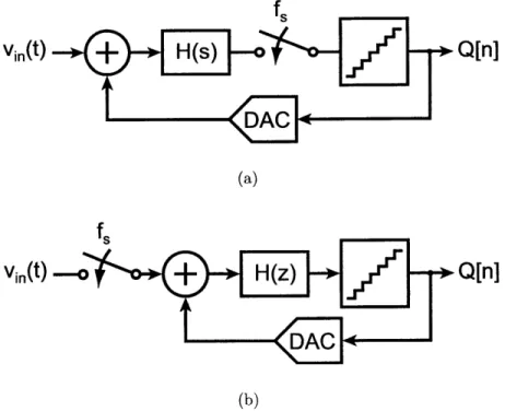
Figure 1-2: (a) inherent anti-alias filtering due to location of sampler after loop filter in a CT AE ADC, and (b) risk of aliasing due to sampling of input-signal without any filtering in a DT AE ADC.
analog signal is first processed by the CT loop filter before being sampled by the quantizer (see Figure 1-2(a)). In contrast, the DT AE samples the input analog signal before it is applied to the loop filter, and therefore requires an explicit anti-alias filter preceding the ADC (see Figure 1-2(b)) [41]. The same is also true for any other DT ADC architecture (SAR, pipeline, flash, etc.), as sampling always occurs prior to the ADC input.
The CT AE ADC's inherent anti-alias filtering ability has also been widely touted in the literature as an elegant architectural means to simplify baseband filtering and digitization in wireless systems [10, 30, 16]. As shown in Figure 1-3(a), a conventional RF receiver would require an explicit low-pass filter prior to the DT ADC (pipeline, DT AE, SAR, flash, etc.) to eliminate out-of-band interferers that would otherwise alias in-band. However, a properly designed CT AE ADC can leverage its inherent anti-aliasing ability to eliminate this low-pass filter, as shown Figure 1-3(b) [10]. Moreover, as scaling yields faster devices, there is even an effort to eliminate the IF
mixer and band-pass (BP) filter by leveraging a BP CT AE ADC to perform filtering and digitization, while performing the final down-conversion in the digital domain with a DSP [16, 30] (see Figure 1-3(c)).
While anti-alias filtering can be performed using off-chip passives, doing so in-creases the system cost and consumes precious real estate on the PCB-an unaccept-able tradeoff in many high volume, ultra-competitive commercial wireless applications where cost and form factor are paramount. Consequently, most recent wireless re-ceiver architectures employing DT ADC's with wide input bandwidths (100 kHz-100 MHz) have opted to perform filtering on chip using active filters [32, 15, 37, 60, 34].
Unfortunately, designing an anti-alias active filter that introduces minimal noise and distortion has the drawback of high power dissipation and area consumption [57]. Indeed, a survey of recently published CT filters (see Table 1.1) has found that the power dissipation can vary from 10 mW to more than 100 mW depending on the desired noise, linearity and bandwidth. At the same time, the active filter's area can vary widely (from 0.1 mm2 to more than 1 mm2) depending on the filter order (with greater than 5th order typical) and the amount of on-chip capacitance (> 100 pF common). Given the considerable power and area overhead involved with designing an explicit anti-alias filter, the inherent filtering ability of the CT AE is very attractive.
Reference Order Bandwidth (MHz) Power (mW) Area (mm2)
[46] 4 60-350 70 0.15 [20] 7 30-100 210 3 [62] 16 0.45 12 2.5 [33] 3 0.93 26 0.5 [44] 10 19 22.5 0.7 [66] 7 1.92 11.6 2.86 [27] 5 2.1 11.6 1.35 [6] 8 15 11.9 Not Reported [4] 6 0.005-5 6.1 1.25 [25] 5 2 10 Not Reported [31] 5 19.7 18 0.32
Table 1.1: brief survey of recently published CT anti-alias filters.
Quadrature IF Mixers
Anti-Alias Discrete-Time ADC Filters (PiDeline. Al. SAR)
Quadrature Continuous-Time
IF Mixers AZ ADC
I
Continuous-Time
BP A ADC
Figure 1-3: prototypical receiver architectures assuming (a) an arbitrary DT ADC preceded by an explicit alias filter (b) a CT AE ADC providing inherent anti-alias filtering, and (c) a bandpass CT AE ADC that eliminates the IF mixer, performs anti-alias filtering at the IF frequency, and downcoverters the IF signal in the digital domain using a DSP.
vin(t)
r--
H (s)
[-o!II
Q[n]
II
I El El 1 11111 IEEE
NRZ DAC Jitter
RZ DAC Jitter
1
Figure 1-4: clock jitter appearing at ADC input due to modulation of charge in a 1-bit NRZ and RZ feedback DAC.
high performance applications was initially met with some skepticism due to con-cerns over the architecture's sensitivity to clock jitter. Indeed, early work on a CT AE ADC's with single-bit quantizers and DAC's [13, 42, 63] showed that such CT architectures were highly sensitive to clock jitter due to the modulation of DAC sig-nal charge appearing directly at the ADC input (see Figure 1-4). In particular, the return-to-zero (RZ) DAC was demonstrated to have far greater jitter sensitivity com-pared to the non-return-to-zero (NRZ) DAC due to its modulation of more than twice the DAC charge at every sample [63]. Consequently, the SNR of these single-bit mod-ulators decreased steadily with increasing clock jitter, typically limiting the converter resolution to no more than 10-11 bits.
Fortunately, recent work has shown that the SNR degradation due to clock jitter can be significantly reduced by pursuing a multibit quantizer and NRZ feedback DAC implementation [64, 36, 50, 65]. As shown in Figure 1-5, jitter now only modulates the DAC charge of the LSB's that change from sample-to-sample. Increasing the number of DAC bits causes jitter to affect a smaller fraction of the DAC full-scale signal, significantly reducing the error charge it introduces. At the same time, improved phase-locked-loop (PLL) design techniques applied to more modern fine line-width technologies have enabled high output clock frequencies with low-jitter performance (< 1 ps,RMS). Indeed, simple PLL architectures achieving GHz output frequencies
3-bit NRZ DAC 4-bit NRZ P DAC 5-bit NRZ DAC
NRZ DAC Output Jitter (Zoom-In)
.. .. ... -4 4 .... .... .... . .. .... .... . . . .. . . . .... . -- -4 4 4 i 4 4 4 ''' '''' '' ' '''''''''''''''' 4'''
Figure 1-5: reducing the amount of charge modulation by clock jitter by increasing the number of bits in a multibit NRZ DAC.
with less than 1 ps,RMS jitter have become quite common in the recent literature [14, 56, 11, 21, 23].
Note, however, that the RZ DAC does have one advantage over its NRZ counter-part. As will be analyzed in greater detail later in this thesis, NRZ multibit DAC's have increased sensitivity to transient mismatches (ISI) but reduced sensitivity to clock jitter, while the opposite is true of RZ structures. It turns out that a dual RZ structure can also be employed to minimize sensitivity to both of these issues. While not implemented in the prototype, we will discuss the dual RZ structure in more detail in Chapter 5.
Given these advancements, modern multibit CT AE ADC implementations with dedicated on-chip PLL's have regularly achieved resolutions rivaling DT equivalents, while avoiding any significant performance limitation due to clock jitter [64, 36, 52, 65]. Indeed, as the industry's interests in CT AE ADC's and greater system in-tegration continues to grow, the emphasis in research has shifted toward exploring new architectures that can continue to deliver high resolution, bandwidth and power efficiency in some the of the latest, deeply submicron technologies [9, 59, 54, 43]. In these highly digital environments, mixed-signal designers of CT AE ADC's (or of
any ADC topology, for that matter) will face new challenges as they strive to build high performance analog circuits while attempting to fully leverage the speed benefits accompanying device scaling.
1.2
Motivations for Investigating VCO-Based ADC's
Voltage controlled oscillator (VCO) based analog-to-digital converters (ADC's) have recently become a topic of great interest in the mixed-signal community [22, 26, 39, 29, 55]. In addition to having a very digital structure that benefits from technology scaling, the VCO presents a host of unique signal processing properties that are especially attractive in the design of oversampling converters. However, certain non-idealities--namely, non-linearity in the VCO's voltage-to-frequency translation-have limited the resolution of the VCO-based ADC to less than 8 effective number of bits (ENOB), pigeon-holing the architecture to niche low-power applications where such resolution is adequate [22, 3]. Indeed, only recently has the mixed-signal community demonstrated that feedback techniques could linearize the VCO-based ADC further, with the work in [55] demonstrating an SNDR of 67 dB in a 20 MHz bandwidth.
To that end, this thesis proposes a new 4th order CT AE ADC architecture that leverages a VCO-based quantizer to achieve 78 dB SNDR in a 20 MHz in-put signal bandwidth. The ADC has an over-sampling ratio (OSR) of 22.5, a 4-bit
quantizer/DAC, consumes approximately 87 mW from a 1.5V supply (FOM = 330
fJ/conv), and is fabricated in a 0.13 pm CMOS process. The primary contributions of this thesis are (1) an architecture that overcomes the severe signal distortion caused by VCO Kv non-linearity, and (2) a methodology for performing first-order dynamic weighted averaging (DWA) on all feedback DAC's. Both of these contributions are essential in order to achieve a resolution > 12 ENOB in a 20 MHz bandwidth.
As a motivation for pursuing a multi-bit VCO-based ADC architecture, this chap-ter will begin by highlighting the unique signal processing properties of VCO's that can be exploited in CT AE ADC design. An overview of prior VCO-based ADC archi-tectures will then be provided, followed by a discussion of non-idealities that limited
VCO Faut
F t (t) = K Vtue (t) Oavtune
Oct(t)
=/
2-rKV,.(t)dt VVo
Figure 1-6: the VCO voltage-to-frequency and voltage-to-phase relationships.
performance. The proposed ADC architecture is then introduced through an example of a 1st order CT AE ADC, which illustrates the significant improvement in linearity
attained by directly leveraging the quantized VCO phase. The simple Ist order case is then expanded to the proposed 4th order CT AE ADC architecture. Finally, the high-speed digital architecture that performs dynamic element matching (DEM) us-ing the DWA technique on all feedback DAC's is presented, with the VCO's unique structure that enables this high-speed technique highlighted. The chapter closes with an outline for the remainder of this thesis.
1.3
Benefits of a VCO-based ADC architecture
While a VCO has a variety of unusual and interesting properties, it has two traits that are especially attractive and relevant in the design of CT AE ADC's. First, the VCO behaves as a CT voltage-to-phase integrator. As shown in Figure 1-6, the instantaneous VCO output frequency F,,t(t) is therefore proportional to the applied input voltage Vtune(t) according to the voltage-to-frequency gain K, [Hz/V]. The resulting VCO output phase Iout (t) is proportional to the time integral of the applied
input voltage. Note that as long as the VCO oscillates, the VCO output phase will accumulate endlessly, even for a DC input. This implies that the VCO behaves as a CT integrator with infinite DC gain.
The value of a simple integrator structure that provides infinite DC gain cannot be emphasized enough. Indeed, with transistor intrinsic gains dropping rapidly at
each technology node, even the ability to achieve modest gains (> 40 dB) with a conventional amplifier topology is far from a trivial exercise, as will be discussed later in this thesis. Note, however, that the VCO integrator is not an ideal integrator even though it has infinite DC gain. Figure 1-6 again illustrates this point by indicating that the VCO output frequency is a non-linear function of the applied input voltage. Consequently, an input voltage signal that modulates the VCO control node will incur potentially high harmonic distortion, degrading the effective dynamic range of the VCO-based integrator.
A second property of interest is the digital nature of a ring-VCO's outputs. Note that while the VCO output phase and frequency are continuously varying, the VCO output itself toggles between two discrete levels, VDD and GND, much like a CMOS digital gate (see Figure 1-7). Multi-phase (or equivalently, multi-bit) quantization can be accomplished by sampling the output phases of a ring oscillator with an array
of D-flip-flops. Note that since the VCO phases are full-swing logic signals, the quantizer is robust to voltage offsets in the flip-flops. At the same time, only one VCO edge transitions at a given sampling instant, while the rest of the VCO phases saturate to either VDD or GND. Consequently, the quantizer not only is less prone to generate metastable outputs, but also has guaranteed monotonicity without requiring any calibration.
The ease with which the VCO's digital output phases can be quantized can be better appreciated when the design of a conventional voltage flash ADC is considered. In the case of a voltage flash, the input signal applied to an array of comparators is typically restricted to be within an operating range, VHI to VLO. Typically, this range is less than the power supply range, VDD to Vss, and is further subdivided according to the number of quantization levels (see Figure 1-8) via a reference ladder. The voltage comparators must then sample and regenerate the resulting signal, which can be on the order of tens of millivolts, and therefore must not only be designed to have high gain and high bandwidth, but also must operate over a wide input common-mode range. To reduce the probability of generating metastable outputs, high-bandwidth preamplifiers typically precede the voltage comparators, consuming additional power.
DFF Array Sampling instant 0out0 Vout0 - -- -- -outO 4 out ---- --- 0 C1out2 >out2 . I out2 --- 1---4out3 4out3 --- --- 1"0 )out4 (*)out4 --- --- 0 0out5 (Iout5 --- 1
out6 Output Range
Vte out6 --- --- 0 (VDD-GND)
Vtune -CIk
Figure 1-7: multibit quantization with a ring oscillator structure.
Finally, since the comparators/preamplifiers can have offset voltages in excess of one or more LSB's, large device sizes must be used to reduce these random offsets to ensure monotonicity. This in turn will also require proportionately larger bias currents in order to maintain the circuit's speed, resulting in both an area and power penalty. While the aforementioned list of design considerations is by no means exhaustive, it is clear that the design of conventional voltage flash quantizers is far from trivial.
1.4
Prior VCO-Based ADC Architectures
The earliest VCO-based ADC was proposed more than thirty years ago for use in a digitally controlled switching regulator [7], and a similar topology was later redis-covered in the superconductivity community five years later [24]. While the exact implementation of the converters differed due to the choice of technology (i.e., semi-conductor vs. supersemi-conductor), the overall architecture for each was essentially the same, and is shown in Figure 1-9(a). Here, the ADC comprises a single-phase output VCO, a counter, and sampling register. As the analog input signal modulates the VCO frequency via the tuning node, the counter continuously accumulates the
-Comparator Preamps ArrayVDD Vref0 Sampling instant refl VHI VHI
Vref2 2refl Vref --...
---... Vref2 -- ---Vref3 Operating Vref4 (VHIVLO) Vref5 in Vref5 Vref6 --- ---VVLO Vref6 GND Vin CIk
Figure 1-8: multibit quantization using a conventional voltage flash architecture.
ber of transitioning edges during the sample period. At the end of the period, the resulting count is sampled by a register, the counter reset to zero, and the process repeated. As can be seen from the figure, the sampled count is proportional to the oscillation frequency of the VCO, and therefore the input signal level.
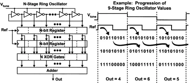
To improve the resolution of the ADC, a ring-oscillator structure was adopted in [22] to generate multiple VCO output phases (see Figure 1-9(b)). Here, each phase output from the ring-VCO drives a counter input, producing a total count with higher resolution than the single-phase VCO-based ADC of [7] and [24]. A serious drawback of this multi-phase approach, however, is that the counter becomes proportionately more complicated to design, and typically consumes greater power and area in order to meet timing and data throughput constraints. At the same time, both the single-phase and multi-single-phase VCO-based ADC must contend with error incurred when the counter misses a VCO edge during reset.
Fortunately, it is possible to eliminate the counters entirely under certain operating
---VCO Vtune Ref Ref Vtune Oscillator Phase I ( I I i a I I r L II/ I 'I i I I I out 5 10 4 7 (a) Ring Oscillator Vtune Ref (b)
Vtune N-Stage Ring Oscillator Example: Progression of
9-Stage Ring Oscillator Values
ReI I
Ref i -bit Registel T a ..
*.* 010110101 :110101010 :101010010 I-bit Registe I , ,101010101 010110101 :110101010: k XOR, Gates , *** $ 111100000 :100011111 011111000: Adder
Out Out=4 Out = 6 Out=5
Figure 1-10: a multi-phase VCO ADC that eliminates the counter by oversampling the VCO phase.
conditions [22]. In particular, when the sample rate is chosen such that the VCO elements do not transition more than once in a given sample period, the counters can be replaced with registers and XOR gates (see Figure 1-10). These gates process the sampled VCO phases, and generate a thermometer code that, when summed, is equivalent to the output count of the counter-based VCO ADC. This equivalence is possible because the register-XOR combination effectively performs a first-order difference, or discrete-time differentiation, of the sampled/quantized VCO phases. Since frequency is the derivative of phase, the resulting outputs will be proportional to the input voltage applied to the VCO control node. Note that the counter-based VCO
ADC's of Figures 1-9(a) and 1-9(b) also performs a first-order difference during reset by effectively subtracting out the previously quantized VCO phase. Consequently, the output count is also proportional to the VCO frequency and to the applied input voltage signal.
A general model for the counter-based and XOR-based VCO ADC architectures is shown in the top-half of Figure 1-11. A subtle benefit of this voltage-to-frequency ADC is that the quantization noise will be first-order noise shaped due to the post-quantization differentiation, as illustrated in Figure 1-11 [22]. Furthermore, the ar-chitecture precludes the feedback DAC needed in a classical first-order AE ADC,
First Order
VCO Quantizer Difference
NN1)mmu4 [n]
r Ref
5
First OrderVCO Sampler Difference
Vue(s) 004((z)) F)
VCO K?
Nonlinearity Quantization Output
Noise Noise
20 dBd
Figure 1-11: analytical model of the voltage-to-frequency VCO ADC, and the equiv-alent frequency domain block diagram.
greatly simplifying design. While the earlier works in [7] and [24] apparently did not recognize the inherent noise-shaping of the voltage-to-frequency VCO ADC, the architecture and its noise-shaping ability was analyzed and tested thoroughly in [22]. As will be discussed next, the non-linearity of the VCO's voltage-to-frequency gain,
K,, severely limits the resolution of this open loop architecture.
For an over-sampling ratio (OSR) of 2000, the AE ADC in [22] achieved a peak SNDR of 71 dB in a 500 Hz bandwidth when the input signal was approximately -36 dBFS. But when the input was increased to -2 dBFS, harmonic distortion arising from
K, non-linearity caused the SNDR to drop down to 44 dB. To mitigate the impact
of this non-linearity, the authors in [22] suggested reducing the maximum allowable input signal such that distortion arising from the K, non-linearity can be minimized. Unfortunately, this solution not only sacrifices a significant amount of DR, but also is not feasible when the desired bandwidth approaches the Megahertz range since such a high OSR is impractical.
Subsequent work sought to suppress the K, non-linearity by embedding the VCO ADC from [22] in the loop filter of a classical AE ADC. A CT AE architecture pro-posed in [26] achieved second-order noise-shaping by preceding the multi-phase VCO
quantizer with an opamp-based integrator, and using a multi-bit feedback DAC. The DT AE architecture in [39] tried to bypass a multi-bit DAC implementation and the required dynamic element matching (DEM) overhead by using a frequency difference detector that pulse-width modulated a one-bit DAC. However, this approach had additional complexities in the frequency difference detector design, and lost the in-herent first-order noise-shaping provided by the VCO quantizer. While both of these architectures intuitively should improve linearity, only behavioral simulation results that tended to downplay or ignore the impact of the K, non-linearity were presented. Consequently, a fair comparison to the work in [22] cannot be made.
Fortunately, a modified version of the ADC in [26] was actually implemented and provided measured results in [55]. As shown in Figure 1-12, this third-order CT AE ADC achieved an extra order of noise shaping without a second op-amp integrator by creating a passive pole with a large on-chip capacitor. At the same time, the architecture in [55] leveraged the algorithm patented in [35] to automatically shape the feedback DAC mismatch by directly connecting the VCO quantizer output bits to the unit elements. As illustrated in Figure 1-12, the scheme leveraged the periodic cycling of ring-VCO delay elements and the inherent VCO integration such that the first-order difference generated the equivalent dynamic weighted averaging (DWA) sequence.
The measured results presented in [55] demonstrated the benefits of using negative feedback with a high gain loop filter to reduce the impact of VCO K, non-linearity. For a signal bandwidth of 20 MHz and an OSR of 25, the CT AZ ADC was able to achieve a peak SNDR of 65.7 dB for a -15 dBFS input signal. This represents a 20 dB improvement compared to the open loop voltage-to-frequency VCO-based ADC from [22]. However, when the signal power was increased to -3 dBFS, distortion tones from K, non-linearity caused the SNDR to drop below 50 dB.
While the brute-force application of higher loop filter gain could help reduce the signal distortion further, a more elegant architecture that can directly address the source of non-linearity is desirable. As will be seen in the next section, simply chang-ing the output variable of interest-from frequency to phase-can effectively eliminate
* I g I Ref I1 01 111100000 100011111 * I )ased Dou -.... Izer& ... .... ....
-Shift V N-Stage Ring Oscillator
Ref -bit Register I
4 I I e-bitRegister SI : XOR Gates: 011111000 ** • " -, 1-Bit PACs
I
DAC OutFigure 1-12: VCO-based ADC that achieved third-order shaping with feedback and an additional passive and active integrator [55].
the impact of signal distortion arising from K, non-linearity.
1.5
Proposed Continuous-Time AE ADC
Archi-tecture
1.5.1
Voltage-to-phase quantization
The previous section revealed that the resolution of prior VCO-based ADC's was primarily limited by distortion arising from the VCO K, non-linearity. While negative feedback techniques did manage to suppress the distortion by more than an order of magnitude, non-linearity still prevented the ADC from achieving its full dynamic range. Consequently, it is clear that a more robust linearization technique is needed
in order to extend the performance and utility of VCO-based quantization.
To that end, this thesis proposes a new VCO-based ADC architecture that over-comes the SNDR limitation imposed by the VCO's non-linear K, characteristic. The
Prior Architectures: Voltage-to-Frequency Quantization
Ring VCO Quantizer
First Order Difference
vN, (t = Vi (t)
./\/"
VCO InputI N It VCO Quantizer
Range :Liv 1 j fOutput Range
I VCO K,
Vtune spans entire input range Nonlinearity Distorted frequency output
(a)
Proposed Architecture: Voltage-to-Phase Quantization
Ring VCO Quantizer Phase
VCO Kv
Vtune a fraction of input range Nonlinearity Undistorted phase output
(b)
Figure 1-13: (a) prior voltage-to-frequency VCO-based ADC architecture that suf-fered from distortion due to K non-linearity, and (b) proposed voltage-to-phase VCO-based ADC that is immune to distortion caused by K non-linearity.
basis for the architecture can be understood by first considering the example of the open-loop first-order CT AE from [22] (see Figure 1-13(a). Here, and in all subse-quently published architectures [26, 55, 3], the VCO output frequency is the desired output variable due to its proportional relationship with the input signal. Therefore, to exercise the full DR of the VCO quantizer, the input signal to the VCO must span the entire non-linear transfer characteristic, and incur harmonic distortion. However, if it were possible to leverage the VCO output phase, then it would not be necessary to span this non-linear transfer characteristic. Since the VCO behaves as an ideal voltage-to-phase integrator and typically has a large K,, small perturbations at the tuning node on the order of tens of mV are sufficient to shift the VCO phase by a substantial amount.
Of course, it is not feasible to use an open-loop integrator with infinite DC gain since frequency offsets, drifts, and temperature variations will cause the VCO output phase to saturate the phase detector that follows. At the same time, the input signal level is restricted to being no more than a few tens of mV, which is a severe restriction on the dynamic range of the ADC. Negative feedback offers a simple solution to this problem, as illustrated in Figure 1-13(b). Here, the VCO phase is sampled and quantized by registers, and compared to a reference phase via a phase detector. The output of the detector then drives a multibit DAC, which subtracts the previously quantized value from the input signal applied to the VCO. The resulting residue is then applied to the control node of the VCO, and integrated during the next cycle.
Note that the feedback loop shown in Figure 1-13(b) is in fact a first-order CT AE ADC loop, and will therefore first-order shape the VCO quantization noise. While this noise-shaping does require a feedback DAC (as opposed to the open-loop noise-shaping achieved in [22]), such a DAC would nonetheless be required in any architecture that embedded the VCO in a higher order AE loop filter, as was done in [26, 55]. As will be explained later in this section, the primary disadvantage of using the VCO output phase instead of frequency is the loss of automatic DWA sequence generation.
As shown in Figures 1-14(a) and 1-14(b), the VCO voltage-to-phase quantizer improves the SNDR of the converter significantly. Here, the ADC's of Figures
1-FFT PLOT on SNDR = 30.7 dB -SNR.=.65:.0dB . ENOB - 4.8 . . . . . . . . . . . . .
i . i
120 -108 107 108ANALOG INPUT FREQUENCY XMHz
FFT PLOT
ANALOG INPUT FREQUENCY XMHz
(b)
Figure 1-14: FFT's generated from the behavioral simulation of the 5-bit (31-stage) VCO-based quantizer assuming (a) the prior voltage-to-frequency and (b) the pro-posed voltage-to-phase architectures. SNDR is calculated over a 20 MHz bandwidth, a -1 dBFS input signal, and a sample rate of 1 GHz.
42 0 20 40 E 60 0 w 0 Z 80 < 100 " 60 0 3 80 -. < 100 120 140 160 180 j : i
I
13(a) and 1-13(b) are modeled and simulated using the CppSim behavioral simulator [48] (a tool that will be described in greater detail in the next chapter), and the corresponding FFT's plotted assuming a -1 dBFS input signal and 1 GHz sample rate. Note that in both cases, VCO non-linearity similar to that in [55] is included in the model by describing the voltage-to-frequency transfer characteristic with a fourth-order polynomial. All other circuit non-idealities are excluded. From Figure 1-14(a), it is obvious that the harmonic distortion in the voltage-to-frequency VCO quantizer of [22, 55] is also present here, limiting the SNDR to roughly 30 dB in a 20 MHz bandwidth. But for the voltage-to-phase VCO quantizer of Figure 1-14(b), the distortion tones are almost completely eliminated. Indeed, the SNDR is limited primarily by the quantization noise, to approximately 66 dB in a 20 MHz bandwidth.
1.5.2
Proposed 4th-order CT AE Loop Filter
The simulation results from the previous section clearly showed the improved linear-ity that can be obtained when using a VCO voltage-to-phase quantizer. In reallinear-ity, thermal noise, DAC mismatch, and other noise and error terms will add on top of the quantization noise floor, further degrading SNDR. To ensure high resolution, it is necessary to expand the loop filter and go beyond first-order noise shaping so that quantization noise can be further suppressed. Ultimately, the converter SNDR should be limited by thermal noise sources, and not by in-band quantization noise.
A fourth-order loop filter was chosen for this thesis due to its high quantization noise shaping ability (SQNR > 95 dB in 20 MHz BW). Traditionally, such a high-order loop filter would be implemented using a cascade of integrators and feed-forward paths, with summation of all signals occurring at the input of the quantizer (see Figure 1-15). This architecture also has the advantage of enabling easy compensation of feedback loop delay by using an additional feedback DAC (labeled DACB in Figure 1-15) around the quantizer to obtain the desired loop filter impulse response [64].
In the proposed architecture, the quantizer is preceded by the VCO voltage-to-phase integrator, precluding the implementation shown in Figure 1-15. Fortunately, the filter can still be realized by replacing one of the feedforward paths with an
![Figure 1-12: VCO-based ADC that achieved third-order shaping with feedback and an additional passive and active integrator [55].](https://thumb-eu.123doks.com/thumbv2/123doknet/13806594.441477/39.918.134.786.105.500/figure-achieved-shaping-feedback-additional-passive-active-integrator.webp)