HAL Id: tel-01862319
https://tel.archives-ouvertes.fr/tel-01862319
Submitted on 27 Aug 2018
HAL is a multi-disciplinary open access
archive for the deposit and dissemination of sci-entific research documents, whether they are pub-lished or not. The documents may come from teaching and research institutions in France or abroad, or from public or private research centers.
L’archive ouverte pluridisciplinaire HAL, est destinée au dépôt et à la diffusion de documents scientifiques de niveau recherche, publiés ou non, émanant des établissements d’enseignement et de recherche français ou étrangers, des laboratoires publics ou privés.
Cecile Nail
To cite this version:
Cecile Nail. Investigation of hybrid CBRAM/OXRAM non-volatile memories for low consumption and high reliability. Micro and nanotechnologies/Microelectronics. Université Grenoble Alpes, 2018. English. �NNT : 2018GREAT010�. �tel-01862319�
DOCTEUR DE LA
COMMUNAUTÉ UNIVERSITÉ GRENOBLE ALPES
Spécialité : NANO ELECTRONIQUE ET NANO TECHNOLOGIES
Arrêté ministériel : 25 mai 2016
Présentée par
Cécile NAIL
Thèse dirigée par Christophe VALLEE, UGA préparée au sein du Laboratoire CEA/LETI
dans l'École Doctorale Electronique, Electrotechnique,
Automatique, Traitement du Signal (EEATS)
Etude de mémoire non-volatile hybride
CBRAM OXRAM pour faible consommation
et forte fiabilité
Investigation of hybrid CBRAM/OXRAM
non-volatile memories for low consumption and
high reliability
Thèse soutenue publiquement le 30 janvier 2018, devant le jury composé de :
Monsieur Christophe VALLEE
Professeur, Université Grenoble Alpes, Directeur de thèse
Monsieur Damien DELERUYELLE
Professeur, INSA Lyon, Rapporteur
Madame Blanka MAGYARI-KOPE
Ingénieur de Recherche, Stanford University, Rapporteur
Monsieur Jeffrey CHILDRESS
Ingénieur, Crocus Technology, Examinateur
Monsieur Francis BALESTRA
Directeur de Recherche, CNRS Délégation Alpes, Président
Monsieur Gabriel MOLAS
As Information Technologies (IT) are still growing, memory devices need to evolve to answer IT market demands. Nowadays, new technologies are emerging and are entering the market. Resistive Random Access Memory (RRAM) are part of these emerging devices and offer great advantages in terms of power consumption, performances, density and the possibility to be integrated in the back end of line. However, to be competitive, some roadblocks still have to be overcome especially regarding technology vari-ability, reliability and thermal stability. Their place on memory market is then still undefined. Moreover, as RRAM working principle depends on stack materials and has to be observed at nanometer resolution, switching mechanism understanding is still challenging. This manuscript proposes an analysis of oxide-based CBRAM microscopic working principle based on electrical characterization results and atomistic simulation. Then, an interdependence between RRAM electrical performances as well as mate-rial parameters is studied to point out new parameters that can be taken into account to target specific memory applications.
This manuscript summarizes a 3 years work done in the CEA-Leti ad-vanced memory technologies laboratory. This Ph.D. thesis was focused on an emerging non–volatile memory technology: the oxide-based Con-ductive Bridge Random Access Memory (CBRAM). With electrical charac-terization and atomistic simulation work, working principle of this device is investigated and material indicator are studied to bring guidance on a material selection or engineering method to target the best material for a given application.
Chapter I will state the work research context, going through the
dif-ferent emerging memories and the current industrial market. As an in-troduction to the rest of the manuscript, this chapter will focus on RRAM potential in terms of performances to integrate stand-alone, or embedded or storage class memories. Moreover, as RRAM working principle under-standing is still challenging, a current state of switching mechanisms com-prehension will be done.
Chapter II will be focused on describing the studied samples and the
characterization methods that will be used to address RRAM behavior. This chapter, will serve as basis to all devices tested and experimental results presented in the following of the manuscript.
Chapter III, similarly to chapter II, will serve as a reference for the
follow-ing of the manuscript regardfollow-ing atomistic simulation to have more insights about oxide-based CBRAM switching mechanism at the microscopic level. It will describe the involved physics in first principle simulation and ex-plain how results will be used and extracted.
Chapter IV will deal with microscopic mechanism in Al2O3-based CBRAM combining electrical characterization and atomistic simulation presented in the two previous chapters. Electrical characterization will be used to study polarization impact on filament formation and atomistic simula-tions will give results on charged species that could be influenced by
elec-tion and simulaelec-tion to compare several RRAM, new parameters that can be taken into account to target specific applications will be pointed out.
Chapter VI will synthesize results presented in this manuscript. It will
focus on mechanisms involved in different oxide-based CBRAM devices and optimization will be discussed in terms of programming conditions and material parameters. Finally, to conclude this work, we will highlight some perspectives to pursue oxide-based CBRAM understanding and tar-get industrial market.
Contents v
List of Figures ix
List of Tables xv
1 RRAM potential in non-volatile memory market: storage class,
stand-alone or embedded product? 1
1.1 Context: Memory market . . . 1
1.1.1 Stand-alone memory: a mature technology . . . 1
1.1.2 Embedded memory: single specifications for each ap-plication . . . 3
1.1.3 Memory hierarchy in computing systems: storage class and working memory . . . 4
1.2 Resistive emerging memories: Principles and characteristics 5 1.2.1 FeRAM . . . 5
1.2.2 MRAM . . . 6
1.2.3 PCRAM . . . 6
1.2.4 RRAM . . . 7
1.2.5 Comparison with actual Flash technologies . . . 7
1.3 RRAM technologies: how does it work? . . . 9
1.3.1 Generalities . . . 9
1.3.2 Advanced understanding on filament formation and composition . . . 9
1.4 Towards RRAM Industrialization: RRAM potential in mem-ory market . . . 14
1.4.1 History . . . 14
1.4.2 RRAM for the actual memory market . . . 15
1.4.3 RRAM improvement: work in research for theoretical understanding. . . 17
2 Studied devices and electrical characterization set up 35 2.1 Introduction/Objectives . . . 35 2.2 Studied Devices . . . 35 2.2.1 Material stacks . . . 35 2.2.2 Integration . . . 36 2.3 Electrical characterization . . . 39 2.3.1 Quasi-static programming . . . 40 2.3.2 pulsed programming . . . 40
2.3.3 RRAM characteristics extraction: endurance, retention and window margin . . . 41
2.4 Chapter II synthesis. . . 44
3 Atomistic simulation 47 3.1 Introduction/Objectives . . . 47
3.2 Density functional theory . . . 48
3.2.1 History . . . 48
3.2.2 Solving Schrödinger equation. . . 49
3.2.3 Practical implementation . . . 51
3.2.4 Structures and defect calculations . . . 53
3.3 Method . . . 56
3.3.1 Thermodynamic of the defects . . . 56
3.3.2 Diffusion of defects . . . 58
3.4 Chapter III synthesis . . . 62
4 RRAM filament composition by atomistic study 65 4.1 Introduction/Objectives . . . 65
4.2 Basic review on RRAM working principle . . . 66
4.3 Experimental observations . . . 66 4.3.1 Studied samples . . . 66 4.3.2 Polarization effect . . . 67 4.4 Simulations . . . 70 4.4.1 Simulation framework . . . 70 4.4.2 Thermodynamic results . . . 72 4.4.3 Amorphous comparison . . . 75 4.4.4 Diffusion in Al2O3 . . . 76 4.5 Al2O3filament formation . . . 79 4.6 Chapter IV synthesis . . . 83
5 RRAM performances trade-off 89 5.1 Introduction/Objectives . . . 89
5.3 Optimizing programming conditions . . . 91
5.4 Endurance vs Window Margin Trade-off . . . 92
5.5 Endurance plus Window Margin improvement vs retention Trade-off . . . 93
5.6 RRAM Filament properties . . . 95
5.6.1 Simulation framework . . . 95
5.6.2 HfO2thermodynamic of defects . . . 96
5.6.3 HfO2defect diffusion. . . 99
5.6.4 Simulation results summary . . . 100
5.7 A link between RRAM performances and material microscopic properties . . . 100
5.7.1 Migration energy barrier correlated to RRAM perfor-mances . . . 100
5.7.2 Qualitative explanation . . . 102
5.7.3 Impact on RRAM material choice . . . 103
5.8 Chapter V synthesis . . . 105
6 Synthesis and perspectives 111 6.1 Objectives . . . 111
6.2 Synthesis and direct perspertives of this work . . . 111
6.2.1 HRRAM microscopic mechanism . . . 111
6.2.2 HRRAM performances linked to microscopic properties113 6.3 General perspertives . . . 115
6.3.1 RRAM understanding . . . 115
6.4 Industrial perspectives . . . 117
6.4.1 Targetting low consumption . . . 117
A Annexes I
A.1 Simulation framework . . . I
A.2 Figures annexes . . . I
1.2 Comparison of Flash memory and hard drive [5]. . . 3
1.3 Memory hierarchy in computers. . . 5
1.4 Current state of the memory technology [7]. . . 5
1.5 Schema of FRAM polarisations [11]. . . 6
1.6 Schema of MRAM two resistive states. . . 7
1.7 Schema of PCRAM working principle. . . 7
1.8 Storage capacity evolution for various non–volatile technolo-gies [17]. . . 8
1.9 schema of CBRAM working principle associated with its elec-trical response. . . 10
1.10 Schemas of electrochemical metallization steps for CBRAM working principle theory. . . 11
1.11 Schemas of oxygen vacancies (VO) displacement at the heart of OxRAM technologies: a) and b) oxygen vacancies redistri-bution in the resistive layer. a’), b’) and c’) oxygen vacancies recombination. . . 12
1.12 Schema of a dielectric current vs time response under con-stant bias. Zone 1: charge absorption, Zone 2: new traps cre-ation, Zone 3: breakdown. . . 14
1.13 RRAM maturity level [71] . . . 17
1.14 Observation of conducting filament dynamics in SiO2-based resistive memories [73]. . . 18
1.15 Activation energies (eV) of VO diffusion on four pathways at different charge states in Al2O3. Al in red, O in white and VO in yellow [77]. . . 20
1.16 Motivation to go from CBRAM/OxRRAM to HRRAM. . . 21
2.1 Stacks variation example studied in this work . . . 36
2.2 Schema of a VIA structure . . . 36
2.3 Schema of a MESA structure . . . 37
2.4 Typical SET and RESET I(V) curve of a) 1R and b) 1T1R W/Al2O3/CuTex device . . . 38
2.5 Schema of 1 Transistor - 1 Resistor (1T1R) configuration . . . 38
2.6 Schema of 1R matrix showing leakage current issue. Cell to program at V in green. Note: V/2 should not affect the cells. . 39
2.7 Schema of 4kb matrix tested in this work . . . 39
2.8 Typical Quasi-static I(V) curves with VForming, VSETand VRESET extraction (W/Al2O3(5nm)/CuTex) [9] . . . 41
2.9 Typical endurance curves up to 108 cycles with 100 read ev-ery decades a) all reading points b) Standard deviation on 100 reading points. Ncycles max represents the maximum num-ber of cycle the device reached (W/HfO2 (5nm)/CuTex with Ic=1mA and tpulse=1µs) . . . 42
2.10 Typical retention curves at a) 130◦C with tfailextraction (stan-dard deviation on 15 devices) b) comparison at 130◦C, 170◦C, 200◦C and c) Arrhenius extrapolation at ten years with acti-vation energy extraction [13] . . . 43
2.11 RON and ROFFdistribution associated with Figure 2.9. Mean value and minimum Window Margin can be extracted . . . . 44
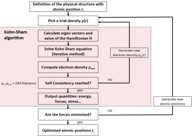
3.1 solving Kohn-Sham equation combined with Force minimiza-tion algorithm. . . 52
3.2 Schema of Al2O3 spinel defective structure. Al in orange, O in pink, vacancies in white. . . 54
3.3 Al2O3 supercell used for calculations. O in red, Al in dark green a) cristaline structure with a densiy of 3.45g.cm–1 b) amorphous structure with a density of 3.1g.cm–1. . . 55
3.4 Illustration of initial and final states calculated to extract de-fect formation energy
∆
H. D+q the defect introduced in the oxide, D the complementary defect introduced in TE, q the charges exchanged. . . 573.5 Example of defect, D, formation energy results with a metal as TE. TE Fermi level is represented and placed on a) with a band alignment shown in b). In a), D+1is the most favorable state if the oxide is in contact with the chosen TE. . . 58
3.6 NEB illustrations. . . 61
3.7 Example of migration barrier with associated path screen shots for a defect D1going to D2. . . 61 4.1 Schematic working principle and I(V) curve Al2O3/CuTexGey
-4.2 Comparison between direct forming F (VTE> 0) and reverse forming F (VTE< 0) for different BE / Al2O3/ CuTexGey struc-tures. . . 68
4.3 I(V) curve and interpretation of a W/Al2O3(3.5nm ALD)/CuTexGey cell being formed by a) reverse forming and then b) 1streset and c) formed again positively before d) and e) standard cycling 69
4.4 Retention comparison between direct F and reverse F
form-ing at 200◦C with ISET=100µA for W/Al2O3ALD 3.5nm/CuTexGey 69 4.5 a) Resistance measurement from 25◦C to 80◦C to extract b)
Energy of electronic transport for different resistances after F and F (W/Al2O3ALD 3.5nm/CuTexGey). . . 70 4.6 γ – Al2O3and a – Al2O3 structure with different copper
inter-stitial positions circled in orange. O in purple, Al in green black, Cu in orange. Cui1 and Cui2 are mentioned and used for migration barrier calculation . . . 71
4.7 Formation enthalpy calculation of intrinsic Al2O3defects. W Fermi level is considered. Yellow zone highlights stoichio-metric Al2O3process conditions. . . 72
4.8 Formation enthalpy calculation of defects in Al2O3/CuTexGey system. Fermi level of 3 types of metal (Pt, W-Cu, Ti-Al) are represented (dashed vertical lines). . . 74
4.9 First principle calculations to compute barrier height to dif-fuse from Cui1 to Cui2 sites (see Figure 4.6) a) Cu+1i in stoi-chiometric or defective Al2O3systems and b) Teiin V–3
Al -rich Al2O3 . . . 77
4.10 Migration barrier in Al2O3 with associated path screen shots of a) VO in red and O–2i in blue by concerted movement, b) Al+3i in red by concerted movements and V–3
Al in blue . . . 78 4.11 Formation enthalpy for different oxides . . . 80
4.12 I(V) curve and interpretation of a W/Al2O3(3.5nm ALD)/CuTexGey cell being formed by a) reverse forming and then b) 1streset and c) formed again positively before d) and e) standard cycling 81
4.13 Illustration of the most energetically favorable exchanges be-tween Al2O3 and CuTexGey during forming and schematic movements happening during forming . . . 83
5.1 Window margin (mean value) as a function of RRAM max-imum achieved cycles reported in literature depending on maximum temperature stability for retention after 24h. . . . 90
5.2 Schematic of the RRAM technologies studied in this work with TEM cross sections of W/HfO2/CuTexbased CBRAM, and EDX (Hf, W, Cu) images. . . 91
5.3 (a) Summary of WM behavior depending on SET current Ic and programming time tprog. Low Ic offers low window mar-gin while high Ic (150µA) degrades ROFF b) Long tprog im-proves the window margin at the expense of lower speed and degraded consumption c) and d) Endurance characteristics of TiN / Al2O3 / CuTex RRAM at 100µA with cycle to cycle Resistance distribution (tSET=tRESET=1µs). Error bars corre-spond to standard deviation measured on 100 subsequent cycles. . . 92
5.4 a) Typical endurance curves with different VRESET to extract b) and c). Impact of VRESET on TiN/Al2O3/CuTexsample on b) ROFF, error bars corresponds to standard deviation on 10 cells and c) endurance (maximum number of achieved cycles). 93
5.5 Endurance and retention performances for a) W/HfO2/CuTex, b) TiN/Al2O3/CuTexand c) TiN/GdOx/CuTex memory tech-nologies. . . 94
5.6 a) Window Margin as function of maximum endurance. For each RRAM technology, various WM were achieved chang-ing the RESET conditions. Gray line is used to extract b) for a constant WM. b) Maximum stable retention temperature af-ter 24h baking time as function of maximum endurance for a given WM (ROFF/RON∼400). . . . 95
5.7 HfO2and a – HfO2structure with different copper interstitial positions. O in red, Hf in blue, Cu in orange. Cui1 and Cui2 are used for migration barrier calculation. . . 96
5.8 Formation enthalpy calculation of defects in HfO2/CuTexGey system. Fermi level of 3 types of metal (Pt, W-Cu, Ti-Al) is represented (dashed vertical lines). . . 97
5.9 Formation enthalpy calculation of defects in HfO2/CuTexGey system. Fermi level of 3 types of metal (Pt, W-Cu, Ti-Al) are represented (dashed vertical lines). . . 98
5.10 First principle calculations to compute the barrier height to diffuse from Cui1to Cui2sites (see Figure 5.7): Cu+1i diffusion barrier in stoichiometric or defective HfO2systems. . . 99
5.11 Emigration impact study on a) endurance with typical curves to extract endurance at diffrent WM and b) retention. Schema
5.12
∆
H impact study on a) endurance and b) retention. . . 1015.13 Migration energy barrier experimental and simulated as a func-tion of maximum endurance. . . 104
5.14 Extraction example of Eexperimentalfor W/HfO2). . . 104
5.15 Radar plot of the performance trade-off for the various RRAM classes reported in this work, and critical key parameters (ma-terial microscopic properties and operating conditions).. . . 106
6.1 a) Window Margin as function of maximum endurance. For each RRAM technology, various WM were achieved chang-ing the RESET conditions. Gray line is used to extract b) for a constant WM. b) Maximum stable retention temperature af-ter 24h baking time as function of maximum endurance for a given WM (ROFF/RON∼400). . . . 113
6.2 Radar plot of the performance trade-off for the various RRAM classes reported in this work, and critical key parameters (ma-terial microscopic properties and operating conditions).. . . 115
6.3 Schematic picture showing the generation of defects and break-down triggering condition in (a) the percolation approach and (b) the new analytic framework presented in [5]. . . 116
6.4 Schema of filament disruption during RESET for WSi and TiN bottom electrode illustrating disruption point and residual filament after RESET . . . 116
1.1 Main differences between stand-alone and embedded flash specifications . . . 4
1.2 Comparison between Flash and emerging memories [7].. . . 8
1.3 RRAM specifications for Storage class applications . . . 16
1.4 RRAM specifications for working memory . . . 16
4.1 Calculated lattice parameters and angles for crytallineγ–Al2O3 and amorphous a – Al2O3structures . . . 71
4.2 Exchange energy
∆
H (eV) between TE and γ-Al2O3. Al2O3 is either stoichiometric or includes oxygen vacancies or alu-minum Frenkel pairs or alualu-minum vacancies . . . 754.3 Formation energies (
∆
H) in stoichiometric or VO-rich a-Al2O3 calculated in GGA considering exchanges with a Cu2Te3Ge Top Electrode . . . 764.4 Summary of DFT calculations, indicating enthalpy formation energy
∆
H, migration energy barrier height Edand hopping distance dh. . . 825.1 Formation enthalpy
∆
H (eV) between the TE and HfO2 ei-ther stoichiometric or including oxygen vacancies . . . 985.2 Formation enthalpy(
∆
H) in a-HfO2stoichiometric or VO-rich calculated in GGA considering exchanges with a Cu2Te3Ge Top Electrode . . . 995.3 Migration energy barrier, Ea, and formation enthalpy,
∆
H, between the TE and different oxides either stoichiometric or including oxygen vacancies (CuiVOdefect). . . 1006.1 Migration energy barrier, Ea, and formation enthalpy,
∆
H, between TE and different oxides either stoichiometric or in-cluding oxygen vacancies (CuiVOdefect). . . 112RRAM potential in non-volatile
memory market: storage class,
stand-alone or embedded
product?
1.1 Context: Memory market
In a world where Information Technologies (IT) are still growing, mem-ory devices need to evolve to answer IT market demands: more data to store, higher speed to access data, less consumption. Resistive Random Access Memories (RRAM) are part of these evaluated technologies to an-swer tomorrow challenges and integrate memory chips. For more clarity, this manuscript starts by presenting the market context and the limitation of the actual technologies. There are three types of memories that can be distinguished in the actual memory market: stand-alone memory to store data with high density and low cost, embedded memories used for embed-ded systems and memory in computing systems hierarchy used to increase speed with a reasonable cost.
1.1.1 Stand-alone memory: a mature technology
Since computers entered our life, the technics used to store information have been shaken up. People want to keep, exchange, data whatever the size: pictures, videos, documents... To answer this demand, a big data storage market has been created and does not stop evolving. Figure1.1a
shows the evolution of data storage since 1986. Although, digital market increase illustrates new technics to store data, offer is still behind customer demands. Due to a strong change in mentality regarding the “Connected
Life [1]" and a great rise in cloud computing [2], the demand of data storage is still exploding today. Figure 1.1billustrates the evolution of digital data created and exchanged over ten years which shows an exponential growth over time.
(a) Evolution of Data storage since 1986
[3]. (b) Evolution of digital data created
and shared from documents to pic-tures to tweets [4]. 2005 2007 2009 2011 2013 2015 0 2 4 6 8 D i g i t a l i n f o r m a t i o n c r e a t e d & s h a r e d ( z e t t a b y t e s ) Year
Dealing with the technologies created to answer storage demands, dig-ital storage (including magnetic hard disk drives (HDD) and optical disc such as CD, DVD, Blu-Ray. . . ) is preeminent. The main requirements for this technology is to be non-volatile memories and to allow reliability and safety of the data for more than 10 years even at the expense of degraded speed. In the 2000’s, stand-alone memory emerged: non-volatile semi-conductor memories called Floating Gate Flash memory. Faster than Hard Drive, it first appeared in USB-keys and then in Solid State Drive (SSD) card because of its high density on a restricted area. Today, complete HDD replacement start to be questioned with SSD introduction in computers, tablet and smartphones. Indeed, with the cost reduction of Flash memory due to its high integration density coupled to similar performances, Flash memory becomes competitive (see Figure1.2).
However, in order to access market demands, this technology follows the Moore law consisting in the doubling of the number of transistors in a dense integrated circuit every two years thanks to a transistor downscal-ing. This constant size reduction of Flash memory cells faces key techno-logical and physical issues including high operation voltage, high power consumption, lithography limitations, tunnel oxide thickness reduction, reduction of the space between cells and diminution of the number of stored electrons [6]. All these technological issues having more and more
Hard Disk Drives (today) flash drives (today) flash drives (tomorrow) Raw capacity 1.72x 1x 1x Access time ~ 1ms ~ 0.3ms ~ 0.1ms Floor space 1.33x 1x 0.66x Energy Usage 13.9kW 5.7kW ~ 5.0kW price 1x 1x <1x
Figure 1.2: Comparison of Flash memory and hard drive [5].
technologies started to grow. Yet, this Flash technology is cheap and ma-ture. A new device will require aggressive specifications especially in terms of density and cost to integrate stand-alone market.
1.1.2 Embedded memory: single specifications for each application
Embedded memory is used for embedded systems which require high speed, wide bus-width capability and low consumption. In order to access this demand, this technology has a dedicated architecture to support the logic core and accomplish intended functions. Compare to stand-alone memory, inter-chip communication are eliminated and the memory ca-pacity is specific for an application. The main disadvantages of embed-ded memories are that they are generally larger in size and are more com-plex to design and manufacture. Additionally, a trade-off must often be found between design and technology since the optimized technology for a memory cell is not the same as that for embedded logic devices. Fur-thermore, processing becomes even more complex when the designer in-tegrates different types of memory on the same chip. Table1.1summarizes the main differences between stand-alone and embedded flash technolo-gies. It can be noted that an embedded memory technoloy requirement is always given for a specific target that could go from automobile to IoT applications. New technologies are welcomed to enlarge possibilities for novel applications.
Table 1.1: Main differences between stand-alone and embedded flash specifications
Embedded stand-alone Main application Code execution File Storage
Storage Capacity Low High
Cost per bit High Low
Active Power High Low
Standby Power Low High
Write Speed Low High
Read Speed High Low
1.1.3 Memory hierarchy in computing systems: storage class and work-ing memory
Going back to the technologies used to answer storage demand, mag-netic hard disk drives (HDD) are preeminents in terms of storage in com-puting systems. HDD allows reliability and safety of the data for more than 10 years. However, this kind of storage class memory is quite slow regarding to processor capabilities (CPU). They have an access time be-tween 0.1ms and 1ms depending on the technology while CPU requires data to be accessible in less than 1ns. In order not to be limited by the speed of these kind of memories, volatile semiconductor devices (based on transistor technology) are used as intermediate between processors and hard disk drives. These working memories need to be fast even at the ex-pense of data retention. Only Static Random Access Memory (SRAM) are fast enough to overcome speed issue but is expensive. Therefore, Dynamic Random Access Memory (DRAM) which is cheaper and with intermediate speed has been introduced in computer memory hierarchy. Compared to non-volatile memory, these two technologies are faster but they lose their information when power supply is shut down. One of the challenges today consists in filling the gap between working memories (DRAM) and storage memories (HDD, SSD) with intermediate density. Indeed, Flash memory has an access time of 100µs and Gigabits can be stored while DRAM has an access time of 10ns and Megabits can be stored (see Figure1.3).
cost ? CPU SRAM DRAM Storage (HDD/SSD) 1ms 1ns Access time 10ns Large gap
Figure 1.3: Memory hierarchy in computers.
1.2 Resistive emerging memories: Principles and
charac-teristics
Figure 1.4 summarizes the current state of semiconductor memory de-vices divided between volatile and non-volatile technologies. We will fo-cus on emerging non-volatile resistive memories. Their working princi-ple relies on having two distinguished resistive states electrically measur-able and commutmeasur-able establishing the so called "0 state" and "1 state" of a memory. Memory state is measured by sensing the current flowing through the device leading to two distinguished electrical responses. These two states need to be repeatable, reversible and reading should be non destructive. Resistive emerging memories show different maturity levels. Some products already exist but they are still considered as emerging mem-ories, as their potential to replace Flash or DRAM has not been clearly demonstrated yet.
Figure 1.4: Current state of the memory technology [7].
1.2.1 FeRAM
The oldest one is the Ferroelectric RAM (FeRAM), which is produced by Fujitsu [8] and Texas Instrument [9] and already on the market. The
working principle of this technology relies on two stable polarization states proper to ferroelectric material. They have an intrinsic electric dipole able to switch depending on an applied electric field allowing to obtain dis-tinguished resistances [10] (see Figure1.5). Therefore, they belong to the switching resistance memory family.
Figure 1.5: Schema of FRAM polarisations [11].
1.2.2 MRAM
Magnetoresistive memory (MRAM) is another emerging technology whose data storage is based this time on the magnetization change of a material layer associated with another layer having a fixed magnetization [12]. If the two layers have the same magnetization, a high current can flow through these two layers. On the contrary if the two layers have an opposite mag-netization the resistance of the device is high (see Figure1.6). The magne-tization change is obtained thanks to an applied magnetic field which can be created by a current. Today, this technology is mainly commercialized by Everspin and a product is announced by Samsung for 2018.
1.2.3 PCRAM
The Phase Change memory (PCRAM) relies on a possible phase change by applying a voltage on the cell. Chalcogenides are the material used
hav-Figure 1.6: Schema of MRAM two resistive states.
resistances [13] (see Figure1.7). Intel associated with Micron announced a a high density product for 2018 based on this technology [14].
Figure 1.7: Schema of PCRAM working principle.
1.2.4 RRAM
Resitive memories are divided in two kinds of technologies: Oxide RAM (OxRAM) and Conductive Bridge RAM (CBRAM). They rely on the forma-tion and disrupforma-tion of a conductive path in a resistive layer. As they are the subject of this manuscript, these technologies will be described in the following.
1.2.5 Comparison with actual Flash technologies
All these technologies show promising performances and may be poten-tial candidate for memory market. Figure1.8 shows the improving matu-rity of emerging technologies compared to Flash in terms of storage
ca-pacity. Table 1.2 summarizes and compare in more details these emerg-ing technologies with Flash memory [7]. RRAM are good competitors and present a great potential especially in terms of high speed, low consump-tion and ease of integraconsump-tion in the Back End Of Line [15, 16]. Compare to DRAM technologies they present a higher density of integration at the expense of speed. A more precise state of the art of the current RRAM per-formances and devices will be given in the following of the chapter.
Figure 1.8: Storage capacity evolution for various non–volatile technologies [17].
Table 1.2: Comparison between Flash and emerging memories [7].
Flash FeRAM PCRAM MRAM RRAM
2013 16 180 45 65 5 Integration F (nm) Projected < 10 65 8 16 < 5 2013 4 22 4 20 4 Cell surface F2 Projected 4 12 4 8 4 2013 15-20 1.3-3.3 3 1.8 0.6 Programming Voltages (V) Projected 15 0.7-1.5 < 3 < 1 < 0.5 2013 1 / 0.1ms 65ns 100ns 35ns < 1ns Programming/Erasing time Projected 1 / 0.1ms < 10ns < 50ns < 1ns < 1ns 2013 4*10–16 3*10–14 6*10–12 2.5*10–12 1*10–12 Programming power (J/bit)
Projected 1*10–16 7*10–15 1*10–15 1.5*10–13 1*10–16 2013 4.5 1.3-3.3 1.2 1.8 0.2 Read Voltage (V) Projected 4.5 0.7-1.5 < 1 < 1 0.1 2013 0.1ms 40ns 12ns 35ns 50ns Read time (ns) Projected 0.1ms < 20ns < 10ns < 20ns < 10ns 2013 10 10 > 10 > 10 < 10
Data retention (year)
Projected 10 10 > 10 > 10 > 10
2013 105 1014 109 1012 1012
Endurance (Cycle)
1.3 RRAM technologies: how does it work?
1.3.1 Generalities
RRAM technologies are based on a Metal/Insulator/Metal (MIM) struc-ture: a thin resistive layer is sandwiched between two metallic electrodes; the Top electrode (TE) and the Bottom electrode (BE) [18] (see Figure1.9a). By applying a voltage between TE and BE, a conductive path, called fila-ment, can be formed linking both electrodes, allowing current to flow and leading to a low resistive state. This phenomenon is stable and reversible by applying another voltage drop on the cell coming back to a high resistive state. Depending on TE nature, this filament can be composed of different species. In CBRAM, filament is composed of metal ions coming from the TE; TE is called "active". In OxRRAM technology, filament is composed of oxygen vacancies created in the oxide resistive layer. In this manuscript we will talk as well about Hybrid Resistive RAM (HRRAM) where filament could be composed of oxygen vacancies and TE metal ions [19–22].
Figure1.9bpresents an electrical response of a typical RRAM with a sim-ple description of CBRAM princisim-ple Figure1.9a. First the cell is in a Pris-tine state; no current has been applied yet. Forming process is the first step the cell sees. Typically, forming voltage is higher than subsequent switch-ing voltage and cell switches from a Pristine state to a Low Resistive State. Then a reverse voltage is applied to the cell which will disrupt the conduc-tive path and lead to a High Resisconduc-tive State. This step is called RESET. A new voltage drop is applied to create the conductive path again and leads to Low Resistive State. This last step is called SET. Switching between SET and RESET is possible as many time as the technology permits it and is called cycling. It can be noted here that in some technologies it is possible to RESET at the same polarity than SET. This process is then called unipo-lar instead of bipounipo-lar in the other case. Switching voltage and time depend on technology (typically ∼2V). The current during SET is limited by an ex-terior device (transistor or diode) to avoid a weariness of the resistive layer which would lead to an early breakdown.
1.3.2 Advanced understanding on filament formation and composition
Conductive path formation is actually more complex than the previous simple description. To describe in more details a conductive path forma-tion, several physical phenomena need to be taken into account. The
fol-(a) CBRAM working principle with fil-ament creation and disruption in or-ange. Top Electrode Bottom Electrode ions On state Top Electrode Bottom Electrode ions Off state Top Electrode Bottom Electrode Resistive layer Pristine state 5nm 20nm Forming Cycling SET RESET I V
(b) Typical IV curve of a bipolar behav-ior for Al2O3(5nm)/Cu CBRAM.
-2 -1 0 1 2 3 4 5 6 10 -14 10 -12 10 -10 10 -8 10 -6 10 -4 V f SET V SET Forming I [ A ] Voltage [V] RESET tool limit
Figure 1.9: schema of CBRAM working principle associated with its electrical response.
lowing descriptions are theoretical and subject to modification as a com-plete physical understanding is still missing.
Metal ion filament
For CBRAM, the switching mechanism is based on the formation and disruption of a metallic filament. This section is deduced to the two main approaches which are currently considered to describe its working princi-ple.
The first approach is the electrochemical metallization (ECM) which is composed of three steps: Oxidation, Migration and Reduction [19,23].
Oxidation consists in ion creation at one of the electrode/resistive layer interface. This electrode has to be electrochemically active and is usually placed as a TE (Silver [24], Copper [25]). Some theory has been supporting this idea based on [23,26].
The second step is an ion migration driven by electric field (created by the voltage drop applied on the cell) towards the second electrode (usually BE). The resistive layer has to be well chosen to allow this migration (for example: GeS2 for Ag [27] or Al2O3 for Cu [28]).
Finally, the ions are reduced and accumulate at the second electrode starting a filament. When enough ions are reduced, the conductive path is created linking top and bottom electrodes. This phenomenon is reversible, with this time, ion creation at the second electrode interface and reduction at the first one. It is essential here that the second electrode is composed
operation what would lead to a non-proper filament erasing. This opera-tion is enhanced by heating due to high current density flowing before the destruction of the conductive path.
Figure 1.10: Schemas of electrochemical metallization steps for CBRAM working principle theory.
In a second approach, atoms are not ionized at electrode/resistive layer interface but there is an electromigration event. The commutation process is based on a momentum transfer between the electrons and the diffusing metal atoms [29,30]. This phenomenon needs a sufficient amount of cur-rent and the feasibility of a non-volatile memory relying on such switching mechanism has been proved [31]. This theory is not accepted as much as the previous one.
Oxygen vacancies filament
For OxRAM, filament creation and disruption are due to oxygen vacan-cies movement. This section is deduced to the two main approaches which are currently considered to describe its working principle.
Oxygen vacancies displacement takes place in transition metal oxide (HfO2, Ta2O5, NiO [32–34]) surrounded by two electrodes. The cells require an oxygen vacancies supplier which can be a particular oxidizable electrode (transition metal such as Hf, Ta, Ti) or a particular resistive layer depleted in oxygen [33, 35, 36]. Today there are two main approaches to explain a switching mechanism based on oxygen vacancies displacements.
A first approach consists in the redistribution of oxygen vacancies al-ready existing in the resistive layer. Enough oxygen vacancies to create
a conductive path are considered already present in the oxide or created during the first writing operation: Forming. These vacancies are charged and migrate under the electric field induced by the applied voltage, creat-ing a filament. The current flowcreat-ing through this path also generates heat enhancing the vacancies migration and filament destruction. In this ap-proach, oxygen vacancies are responsible for the electrical conduction and their migration induced by the electric field explains the bipolar switching.
Figure 1.11: Schemas of oxygen vacancies (VO) displacement at the heart of OxRAM technologies:
a) and b) oxygen vacancies redistribution in the resistive layer. a’), b’) and c’) oxygen vacancies recombination.
Another approach is based on the creation and destruction of oxygen vacancies [37] at each cycle and not only during Forming. Local redox re-actions of the resistive layer can modify the vacancies concentration ing SET or RESET. Thus, this metal oxide is reduced at its metal state dur-ing SET creatdur-ing a conductive path rich in metal. Durdur-ing RESET, the same atoms are oxidized decreasing the metal concentration. Both processes are accelerated by the thermal heating induced by the high current density. In this approach, the conductive path is formed by a decrease of oxygen con-centration and increase of metal content. The bipolarity of the switching mechanism is explained by the difference of voltage favoring either the ox-ide reduction or metal oxidation. A unipolar switching is also possible if the RESET operation is only thermally driven.
Oxygen vacancies displacement is at the heart of OxRAM technologies also called as valence change memory (VCM). Figure 11 shows a schematic
Resistance change
RRAM working principle is based on cell resistance change depending on the amount of current flowing. There are several hypotheses to explain oxygen vacancies and metal ions electrical conduction. Depending on re-sistive state (high or low) different mechanism are invoked.
In the case of metal ion conductive path, standard Ohm conduction is generally employed [37,38]. This conduction form is also used to simplify the HRS electrical conduction but with a strongly reduced conductivity. It is important to note that it exists a continuum [39] of states between a fully formed filament in LRS and a fully dissolved in HRS. During the early stages of RESET, the filament thickness is greatly reduced at a constriction point. Once the constriction is small enough (few atoms), the electrical conduction can be tied to a Quantum Point Contact conduction [40–42]. This conduction is attributed to the very low amount of atoms allowing the current to flow, resulting in a quantum conduction in one dimension. Fol-lowing the filament dissolution, shortly after it breaks and a gap appears between both top and bottom side of the filament, in this case the conduc-tion can be explained by Fowler–Nordheim tunneling [43, 44]. With the RESET progression, the gap increases and charge trap might appear in the gap during the process. The last conduction model, bonded to theses traps relies on Trap Assisted Tunneling (TAT) [45–47]. It can be noted as well that some study has been performed on oxide dealing with filament formation due to sub-oxides [48].
Dielectric breakdown
OxRAM technology is based on the reversible creation of oxygen vacan-cies in a dielectric such as HfO2, Al2O3... A parallel can be made with oxide breakdown. For a dielectric, one of its main property is to not conduct the current. When a potential difference is applied to a dielectric, a leakage current is observed. This is due do charge traps already present post pro-cess and allow a small current path. For a good insulator, this current is of the order of 10–12A. Figure 1.12presents a dielectric current evolution over time when this one is under a constant bias. This curve can be cut in 3 different zones.
In zone 1, the current is decreasing over time representing the absorp-tion of charges that the dielectric can sustain due to its own charge traps.
In zone 2, current is increasing demonstrating a creation of new traps, defects, to allow current flow.
This phenomenon gets out of control zone 3, where an avalanche of defect creation happens and leads to breakdown meaning the dielectric becomes conductor [20]. This breakdown can be controlled if a limited amount of current is permitted by an exterior device. In this case, some of the traps can be annihilated. RRAM forming step can be correlated to this description (see Figure 1.9b). Some device models use this knowledge to put in equation RRAM behavior especially using a percolation model [49].
Figure 1.12: Schema of a dielectric current vs time response under constant bias. Zone 1: charge absorption, Zone 2: new traps creation, Zone 3: breakdown.
1.4 Towards RRAM Industrialization: RRAM potential in
mem-ory market
1.4.1 History
The first migration of silver ion in a porous material has been published in 1954 [50]. Putting a potential difference on a material sandwiched by two Ag electrodes, Ag migration is observed. But a memory device is not
yet in the idea. In 1964, memory effect is demonstrated in a metal/insulator/metal (MIM) structure, namely Au/SiO/Au [51]. At the time it was hypothesized
that such a structure could have been used as a memory device which could be accessed non-destructively. In the ensuing years similar phe-nomena were found in an Al/SiOx/Au system [52,53]. Due to stability is-sues and the successful development of Si based memories [54], resistive
In 2002, W.W. Zhuang et al. demonstrated an RRAM device based on PCMO which could have greater performances than Flash devices [55]. In 2004, Samsung Electronics demonstrated resistive switching behavior in various transition metal oxides (TMO) such as NiO, TiO2, HfO2 and ZrO2 with promising characteristics such as an operating voltage below 3V, a programming current around 2mA and an endurance of 106 cycles [56]. In parallel, memory effect are published using metal ion migration.
For CBRAM, the first researches were mostly devoted to a large screen-ing of the material combinations offerscreen-ing the switchscreen-ing mechanisms by metal migration in a resistive layer. For this matter, a great interest on the use of chalcogenide has grown and a lot of researches were presented on various resistive layers and electrodes combinations. For example GeTe [57], GST [58], ZnxCd1–xS [59,60] or Cu2S [61,62]. GexSy and GexSey were the two most studied components mainly coupled with silver top electrode but various bottom electrodes such as Tungsten, Platinium or Nickel [63]. This technology was growing in interest but limitations appeared. Tem-perature stability was one of the most important as it can limit CBRAM integration in CMOS integrated circuits due to the high temperatures used in standard back-end-of-line processing. More research intend to improve its stability using different chalcogenide stoichiometry or doping [64] but a big change appeared when the resistive layer was replaced by an oxide.
Oxide offers a higher thermal stability and is a well-known material in microelectronic which will help process integration. The materials screen-ing researches has thus been conducted on oxides such as Al2O3, Ta2O5, HfO2, mainly coupled with copper top electrode.
1.4.2 RRAM for the actual memory market
To emerge in memory market, one need to think about the place of RRAM and its specifications depending on the target. Several memory architec-tures could be considered depending on technology performances and cost.
RRAM for Stand-alone application
As flash devices start to face key technological issues, alternative mem-ory is envisaged. However, as this technology is cheap and mature, ag-gressive specifications in terms of cost and density are required. RRAM advancement for stand-alone applications were presented in [16, 65] but
RRAM technologies face difficulties to reach flash maturity. Moreover, al-though 2D flash topological method is expected to reach its practical limit by 2020, 3D flash technology starts to emerged and will lead the semi-conductor industry towards the next revolution in transistor density [14]. RRAM technology is not expected anymore for stand-alone application unless a major breakthrough occurs.
RRAM for Embedded application
Another idea is to target embedded market. As presented in the begin-ning of the chapter, each application will need specific criteria. RRAM technology already prove its potential for this market. For automotive ap-plication, high temperature stability is required and is demonstrated in [15,66,67]. For low power application, [28,68] can be cited.
RRAM for computing systems hierarchy
The last market RRAM could integrate would be in computing systems hierarchy as a storage class memory (like HDD) or as a working memory (like DRAM). In terms of storage, there are two possibilities: placing RRAM between hard disk and DRAM or replacing hard disk (see Table 1.3). To access this market, RRAM would need to reach a retention stability over 10 years at 85◦C, a latency below 5µs and an endurance superior to 106 with high density product. RRAM advancement for storage class applications were presented in [16,65].
Table 1.3: RRAM specifications for Storage class applications
class memory type latency Endurance Retention Cost Power consumption storage replacing hard disk < 5µs > 106 10years 85◦C < 2 ∗ flash < flash storage between hard disk and DRAM < 5µs > 106 10years 85◦C ∼ flash < flash
In a second case, RRAM could replace or support DRAM. It would then need a latency lower than 50ns as demonstrated in [28,69], retention around few days is enough and a great endurance as demonstrated in [33,70] (see Table1.4).
Table 1.4: RRAM specifications for working memory
class memory type latency Endurance Retention Cost Power consumption working memory replacing DRAM < 50ns > 109 > 5days 85◦C <12DRAM < DRAM working memory between hard disk and DRAM < 200ns > 109 > 5days 85◦C <1
Nowadays, RRAM show some limitations before being able to integrate this market. Four issues remain challenging: window margin variability, forming operation, programming current and trade-off between endurance and retention. Today, the main research efforts have been focused on im-proving device performances, dimensions and physical understanding, plac-ing RRAM technology after the peak of its interest (see Figure 1.13). Re-search is now waiting for an industrial to challenge the technology.
expectations time On the Rise At the Peak Sliding Into The Trough Climbing The Slope Entering The Plateau R&D Startup companies first round of venture
capital funding First-generation products, high price, lots of customization needed Early adopters investigate Mass media hype begins Supplier proliferation Activity beyond Early adopters Negative press begins Supplier consolidation and failures Second/third rounds of venture capital funding Less than 5% of the potential audience
has adopted fully
Second-generation products, some services
Methodologies and best practices developing
Third-generation products, out of the box, product
suites
High-growth adoption phase starts: 20% to 30%
of the potential audience has adopted
the innovation Technology Trigger Peak of Inflated Expectations Trough of Disillusionment Slope of Enlightenment Plateau of Productivity
RRAM
Figure 1.13: RRAM maturity level [71]
1.4.3 RRAM improvement: work in research for theoretical understand-ing
Microscopic observation
Following CMOS development tracks, RRAM presents a lack of theoret-ical bases. The working principle is not yet fully understood and some re-searches are devoted to physically observe RRAM switching mechanism. However, as conductive paths width is supposed to be in nanometer range, literature does not give entire satisfaction. Research is still devoted to RRAM observation, dreaming of a device real-time switch movie with in-situ trans-mission electron microscopy (TEM).
For example in 2011, B. Cho showed a bistable switching mechanism behavior related to the formation and rupture of highly conductive paths in a Ag/polymerstructure using TEM and energy-dispersive X-ray spec-troscopy [72] following in 2012 by Y. Yang et al who published a direct TEM imaging of metal ion/oxide structures showing a metallic conductive path [73]. These results comforted CBRAM principle with a filament composed of metal ions coming from an active electrode which can be formed and disrupted with a bipolar behavior.
In parallel, Q.Liu et al observed in real time a growth and dissolution of conductive filaments in Oxide-Electrolyte-Based RRAM supporting its working principle description: there was no silver in the Pristine state while after forming, Ag is highly detected. After Reset, there is still some Ag de-tected but in lower concentration showing that the initial state is not recov-ered. There is a multifilamentary observation. Conductive filaments are found to start growing from the TE rather than having to reach the BE and grow backwards and have a conical base at the TE interface [74]. This re-sult allows to give a filament shape closer to reality for simulation although it is still in debate.
More recently, in 2014, U. Celano et al used conductive atomic force mi-croscopy to observe the conductive zones in a switched device. They ex-trapolated the results in a 3D image showing a conical filament with its base at the TE. They showed as well, using scanning probe microscopy (SPM), that the constriction of the CFs is below 10 x 10 nm2 indicating a strong scalability potential for OxRAM devices [75,76].
Simulation and Modelling
To support microscopic observation, simulation works are carried out. Among these researches, a lot of effort are put into first principles cal-culations which allow the computation of various properties (electronic, mechanical, energetic. . . ) of a material. However, these calculations are strongly limited by the number of atoms it can simulate. Only few atoms can be simulated in a relative short time duration (few days to weeks), which makes it impossible to simulate a whole RRAM cell. However, it can give insights on defects creation and behavior in one of the layer. For ex-ample, defect energy levels and defect energy migration barriers can be extracted. To give an example of the impact of these works, we can focus on Al2O3as a resistive layer.
To study a possible filament composed of oxygen vacancies, VOdiffusion has been studied for different charge state [77] with a description of defect levels [78,79] giving an idea on the energy cost of creating this filament.
On the other hand, K. Sankaran et al studied in an amorphous Al2O3 the diffusion barrier of different defects such as Cu and Te showing a very low Cu diffusion barrier in the case of porous Al2O3[80] accentuating on a CBRAM behavior study and support a Cu filament.
To go further, J. A. Dawson and J.Robertson use three different filament models in Al2O3, showing that the strong binding between Cu interstitials drives filament formation, resulting in Al ions being driven out of the Cu-rich environment [81]. This result gives insight on a copper based filament formation.
In the same idea, X. Xu et al compared different Cu filament density (3 to 7 atoms of Cu) and show that small changes in the filament structure can lead to large changes in the current-voltage characteristic in atomic scale filaments which can explain a multi-level resistances in RRAM [82].
Staying in electrical characteristics, T.V. Perevalov et al show that elec-tron and hole capture on oxygen vacancy in γ – Al2O3 is an energetically favorable process [83].
Figure 1.15: Activation energies (eV) of VOdiffusion on four pathways at different charge states in
Al2O3. Al in red, O in white and VOin yellow [77].
These studies can be done on other material such as HfO2[84–87], Ta2O5 [88–90]... to comfort or refute some hypothesis following a microscopic observation or an electrical behavior. Moreover, using these calculation results and experimental inputs, device models have been developed fol-lowing various electrical conduction hypothesis such as Ohmic current through highly resistive layer [37,38,91], Fowler-Nordheim tunneling [43,
44], Trap Assisted Tunneling [45–47] or Quantum-Point-Contact [40–42].
From CBRAM/OxRRAM to Hybrid RAM
Most of the results presented in this manuscript were obtained on oxide-based CBRAM. This technology has been motivated by the complementary advantages of chalcogenide CBRAM and OxRRAM. Chalcogenide CBRAM technology is well known for having a high ROFF/RONratio and a low power consumption while OxRRAM has a high temperature stability and high cy-cling. By combining both technologies, having an oxide as resistive layer and an active Top Electrode, this new device may allow to obtain all advan-tages in one technology. However, understanding the working principle of this oxide-based CBRAM is even more challenging. They may combine oxygen vacancy and metal ion movements if TE/oxide are well chosen. In this case, we will talk about Hybrid RRAM (HRRAM) in this manuscript.
Figure 1.16: Motivation to go from CBRAM/OxRRAM to HRRAM.
1.5 Chapter I synthesis
RRAM technologies present great advantages to enter the memory mar-ket thanks to ease of integration in the Back end of Line and high density. They could integrate three different kinds of market: storage class, stand-alone applications and embedded systems. For each target, different spec-ifications are needed. Some of them were demonstrated in literature but RRAM still present some technological issues which place RRAM after its peak of interest, waiting for an industrial to challenge the technology.
Today, various physical mechanisms can explain CBRAM and OxRRAM switching behavior. They rely on a conductive path formation and disrup-tion, called filament, in a resistive layer. In the case of CBRAM, filament is composed of metallic elements coming from the active top electrode while in OxRRAM, it is composed of oxygen vacancies created in the ox-ide resistive layer. At the beginning of CBRAM technology, chalcogenox-ides such as GeS2was chosen with mainly Ag as active top electrode. However, due to high temperature stability issues and hoping to improve window margin and power consumption compare to OxRRAM technology, oxide-based CBRAM were tested. In this case, filament can be composed of oxy-gen vacancies and top electrode metallic element. Our laboratory baptized this technology, combining both type of filament, Hybrid RRAM (HRRAM). This transition to HRRAM brought new challenges to overcome such as higher voltages and higher forming step than CBRAM and endurance can be degraded compare to OxRRAM. Optimization of this technology is still on going and in the same time, as physical understanding is lacking,
mi-croscopic observation and simulations bring more and more knowledge concerning switching mechanism and material properties impact for each stack layer.
In order to optimize HRRAM materials, simulation and electrical char-acterization are carried out in parallel in CEA-Leti. Simulations support or refute hypothesis brought by experimental results to clarify RRAM work-ing principle and evaluate material properties impact on the stacks. In this manuscript, both skills has been developed to combine atomistic simula-tion and electrical characterizasimula-tion. Various RRAM performances are eval-uated to target different types of market from storage to embedded. OxR-RAM and HROxR-RAM are characterized considering several oxygen density. Then, material properties are investigated by atomistic simulation giving microscopic parameters to link RRAM performances and chosen materi-als.
To introduce this work, next chapter will describe the studied samples and the characterization methods that has been used to evaluate RRAM performances. Then, third chapter will explain atomistic simulation the-ory basis and used methods to extract RRAM microscopic properties. These two chapters will serve as basis to the results presented in the following of the manuscript. Then, in the fourth chapter we will present the result on filament microscopic understanding combining experimental and simula-tion results. Chaper five will fully developed microscopic properties effect on HRRAM performances and present some technological key to choose materials for a given application. Finally, chapter six will synthesis and give the perspectives of this work.
[1] T. Global. Connected Life, connectedlife.tnsglobal.com, 2016. 2
[2] M. Armbrust, A. Fox, R. Griffith, A. D. Joseph, R. Katz, A. Konwinski, G. Lee, D. Patterson, A. Rabkin, I. Stoica, and M. Zaharia. A View of Cloud Computing. Commun. ACM, 53(4):50–58, April 2010. doi: 10.1145/1721654.1721672. 2
[3] M. Hilbert. The World’s Technological Capacity to Store, Communi-cate, and Compute Information, 2011. 2
[4] KPCB. Internet Trends Report, http://www.kpcb.com/blog/2016-internet-trends-report, 2016. 2
[5] A. Osys. Flash Storage Trends, https://www.slideshare.net/OsysAG/flash-storage-werner-eggli-osys-tech-talk. ix,3
[6] Y.-H. Shih. 3d Charge Trapping (CT) NAND Flash, http://www.sematech.org/meetings/archives/symposia/10187/, 2011. 2
[7] ITRS. Emerging research devices, 2013. ix,xv,2,5,8
[8] Fujitsu. Fujitsu and Tokyo Institute of Technology Announce the De-velopment of New Material for 256mbit FeRAM Using 65-nanometer Technology - Fujitsu United States, 2006. 5
[9] T. Instrument. FRAM – New Generation of Non-Volatile Memory, 2008. 5
[10] C. Muller. Mémoires ferroélectriques FRAM : principe, limitations, innovations, applications. Hermès science, pages 425–451, 2011. 6
[11] FRAM | Ferroelectric RAM Technology | Theory & Operation. ix,6
[12] M. Julliere. Tunneling between ferromagnetic films. Physics Letters A, 54(3):225–226, September 1975. doi: 10.1016/0375-9601(75)90174-7.
[13] M. Wuttig and N. Yamada. Phase-change materials for rewriteable data storage. Nature Materials, 6(11):824–832, November 2007. doi: 10.1038/nmat2009. 7
[14] ITRS. Executive Report, 2015. 7,16
[15] J. R. Jameson, P. Blanchard, C. Cheng, J. Dinh, A. Gallo, V. Gopalakr-ishnan, C. Gopalan, B. Guichet, S. Hsu, D. Kamalanathan, D. Kim, F. Koushan, M. Kwan, K. Law, D. Lewis, Y. Ma, V. McCaffrey, S. Park, S. Puthenthermadam, E. Runnion, J. Sanchez, J. Shields, K. Tsai, A. Tysdal, D. Wang, R. Williams, M. N. Kozicki, J. Wang, V. Gopinath, S. Hollmer, and M. V. Buskirk. Conductive-bridge memory (CBRAM) with excellent high-temperature retention. In 2013 IEEE International
Electron Devices Meeting, pages 30.1.1–30.1.4, December 2013. doi:
10.1109/IEDM.2013.6724721. 8,16
[16] S. Sills, S. Yasuda, J. Strand, A. Calderoni, K. Aratani, A. Johnson, and N. Ramaswamy. A copper ReRAM cell for Storage Class Mem-ory applications. In 2014 Symposium on VLSI Technology
(VLSI-Technology): Digest of Technical Papers, pages 1–2, June 2014. doi:
10.1109/VLSIT.2014.6894368. 8,15,16
[17] ISSCC. MEMORY – 2013 Trends. International Solid-State Circuits
Conference, February 2013. ix,8
[18] S. Menzel, U. Böttger, M. Wimmer, and M. Salinga. Physics of the Switching Kinetics in Resistive Memories. Advanced
Func-tional Materials, 25(40):6306–6325, October 2015. doi: http:
//onlinelibrary.wiley.com/doi/10.1002/adfm.201500825/abstract. 9
[19] R. Waser, R. Dittmann, G. Staikov, and K. Szot. Redox-Based Resistive Switching Memories – Nanoionic Mechanisms, Prospects, and Chal-lenges. Advanced Materials, 21(25-26):2632–2663, July 2009. doi: http: //onlinelibrary.wiley.com/doi/10.1002/adma.200900375/abstract. 9,
10
[20] M. Saadi, P. Gonon, C. Vallée, C. Mannequin, H. Grampeix, E. Jalaguier, F. Jomni, and A. Bsiesy. On the mechanisms of cation injection in conducting bridge memories: The case of HfO2 in contact with noble metal anodes (Au, Cu, Ag).
Jour-nal of Applied Physics, 119(11):114501, March 2016. doi: http:
[21] G. Molas, E. Vianello, F. Dahmani, M. Barci, P. Blaise, J. Guy, A. Tof-foli, M. Bernard, A. Roule, F. Pierre, C. Licitra, B. D. Salvo, and L. Perniola. Controlling oxygen vacancies in doped oxide based CBRAM for improved memory performances. In 2014 IEEE
Interna-tional Electron Devices Meeting, pages 6.1.1–6.1.4, December 2014.
doi: 10.1109/IEDM.2014.7046993.
[22] C. Nail, G. Molas, P. Blaise, G. Piccolboni, B. Sklenard, C. Cagli, M. Bernard, A. Roule, M. Azzaz, E. Vianello, C. Carabasse, R. Berthier, D. Cooper, C. Pelissier, T. Magis, G. Ghibaudo, C. Vallée, D. Be-deau, O. Mosendz, B. D. Salvo, and L. Perniola. Understanding RRAM endurance, retention and window margin trade-off using ex-perimental results and simulations. In 2016 IEEE International
Elec-tron Devices Meeting (IEDM), pages 4.5.1–4.5.4, December 2016. doi:
10.1109/IEDM.2016.7838346. 9
[23] I. Valov, I. Sapezanskaia, A. Nayak, T. Tsuruoka, T. Bredow, T. Hasegawa, G. Staikov, M. Aono, and R. Waser. Atomically controlled electrochemical nucleation at superionic solid electrolyte surfaces.
Nature Materials, 11(6):530–535, June 2012. doi: 10.1038/nmat3307. 10
[24] S. Z. Rahaman, S. Maikap, W. S. Chen, H. Y. Lee, F. T. Chen, T. C. Tien, and M. J. Tsai. Impact of TaOx nanolayer at the GeSex/W interface on resistive switching memory performance and investigation of Cu nanofilament. Journal of Applied Physics, 111(6):063710, March 2012. doi: 10.1063/1.3696972. 10
[25] S. Maikap, S. Z. Rahaman, T. Y. Wu, F. Chen, M. J. Kao, and M. J. Tsai. Low current (5 pA) resistive switching memory using high-k Ta2o5 solid electrolyte. In 2009 Proceedings of the European Solid State
Device Research Conference, pages 217–220, September 2009. doi:
10.1109/ESSDERC.2009.5331517. 10
[26] A. Chen, J. Hutchby, V. Zhirnov, G. Bourianoff, and J. . S. Wiley. Emerg-ing Nanoelectronic Devices, 2015. 10
[27] J. R. Jameson, N. Gilbert, F. Koushan, J. Saenz, J. Wang, S. Hollmer, M. Kozicki, and N. Derhacobian. Quantized Con-ductance in Ag/GeS_2/W Conductive-Bridge Memory Cells.
IEEE Electron Device Letters, 33(2):257–259, February 2012. doi:
[28] A. Belmonte, W. Kim, B. Chan, N. Heylen, A. Fantini, M. Houssa, M. Jurczak, and L. Goux. 90nm WAl2o3tiwcu 1t1r CBRAM cell showing low-power, fast and disturb-free operation. In 2013 5th
IEEE International Memory Workshop, pages 26–29, May 2013. doi:
10.1109/IMW.2013.6582089. 10,16
[29] H. Suga, T. Sumiya, M. Horikawa, S. Kumaragurubaran, T. Shimizu, and Y. Naitoh. Threshold Current Density of the Resistance Switching in Pt Nanogap Electrode. Japanese Journal of Applied Physics, 50(6S): 06GF11, June 2011. doi: 10.1143/JJAP.50.06GF11. 11
[30] D. O. Bellisario, Z. Ulissi, and M. S. Strano. A Quantitative and Predictive Model of Electromigration-Induced Breakdown of Metal Nanowires. The Journal of Physical Chemistry C, 117(23):12373–12378, June 2013. doi: 10.1021/jp4035776. 11
[31] T. Takahashi, S. Furuta, Y. Masuda, S. Kumaragurubaran, T. Sumiya, M. Ono, Y. Hayashi, T. Shimizu, H. Suga, M. Horikawa, and Y. Naitoh. 4kb nonvolatile nanogap memory (NGpM) with 1 ns programming capability. In 2012 IEEE Silicon Nanoelectronics Workshop (SNW), pages 1–2, June 2012. doi: 10.1109/SNW.2012.6243334. 11
[32] B. Govoreanu, G. S. Kar, Y. Y. Chen, V. Paraschiv, S. Kubicek, A. Fantini, I. P. Radu, L. Goux, S. Clima, R. Degraeve, N. Jossart, O. Richard, T. Van-deweyer, K. Seo, P. Hendrickx, G. Pourtois, H. Bender, L. Altimime, D. J. Wouters, J. A. Kittl, and M. Jurczak. 10x10nm2 Hf/HfOx crossbar resis-tive RAM with excellent performance, reliability and low-energy op-eration. In 2011 International Electron Devices Meeting, pages 31.6.1– 31.6.4, December 2011. doi: 10.1109/IEDM.2011.6131652. 11
[33] M.-J. Lee, C. B. Lee, D. Lee, S. R. Lee, M. Chang, J. H. Hur, Y.-B. Kim, C.-J. Kim, D. H. Seo, S. Seo, U.-I. Chung, I.-K. Yoo, and K. Kim. A fast, high-endurance and scalable non-volatile memory device made from asymmetric Ta2o(5-x)/TaO(2-x) bilayer structures. Nature Materials, 10(8):625–630, July 2011. doi: 10.1038/nmat3070. 11,16
[34] L. Courtade, C. Turquat, C. Muller, J. G. Lisoni, L. Goux, D. J. Wouters, D. Goguenheim, P. Roussel, and L. Ortega. Oxidation ki-netics of Ni metallic films: Formation of NiO-based resistive switch-ing structures. Thin Solid Films, 516(12):4083–4092, April 2008. doi: 10.1016/j.tsf.2007.09.050. 11
Kwong. The Role of Ti Capping Layer in HfOx-Based RRAM Devices.
IEEE Electron Device Letters, 35(9):912–914, September 2014. doi:
10.1109/LED.2014.2334311. 11
[36] Y. Y. Chen, L. Goux, S. Clima, B. Govoreanu, R. Degraeve, G. S. Kar, A. Fantini, G. Groeseneken, D. J. Wouters, and M. Jurczak. En-durance/Retention Trade-off on HfO2/Metal Cap 1t1r Bipolar RRAM.
IEEE Transactions on Electron Devices, 60(3):1114–1121, March 2013.
doi: 10.1109/TED.2013.2241064. 11
[37] M. Bocquet, D. Deleruyelle, H. Aziza, C. Muller, J. M. Portal, T. Cabout, and E. Jalaguier. Robust Compact Model for Bipolar Oxide-Based Re-sistive Switching Memories. IEEE Transactions on Electron Devices, 61 (3):674–681, March 2014. doi: 10.1109/TED.2013.2296793. 12,13,20
[38] S. Larentis, F. Nardi, S. Balatti, D. C. Gilmer, and D. Ielmini. Resis-tive Switching by Voltage-Driven Ion Migration in Bipolar RRAM-Part II: Modeling. IEEE Transactions on Electron Devices, 59(9):2468–2475, September 2012. doi: 10.1109/TED.2012.2202320. 13,20
[39] L. Goux, K. Sankaran, G. Kar, N. Jossart, K. Opsomer, R. Degraeve, G. Pourtois, G. M. Rignanese, C. Detavernier, S. Clima, Y. Y. Chen, A. Fantini, B. Govoreanu, D. J. Wouters, M. Jurczak, L. Altimime, and J. A. Kittl. Field-driven ultrafast sub-ns programming in WAl2o3ticute-based 1t1r CBRAM system. In 2012 Symposium on VLSI Technology
(VLSIT), pages 69–70, June 2012. doi: 10.1109/VLSIT.2012.6242465. 13
[40] J. Suñé, S. Long, C. Cagli, L. Perniola, X. Lian, X. Cartoixà, R. Rurali, E. Miranda, D. Jiménez, and M. Liu. Electrical evidence of atomic-size effects in the conduction filament of RRAM. In 2012 IEEE 11th
Inter-national Conference on Solid-State and Integrated Circuit Technology,
pages 1–4, October 2012. doi: 10.1109/ICSICT.2012.6467649. 13,20
[41] R. Degraeve, A. Fantini, S. Clima, B. Govoreanu, L. Goux, Y. Y. Chen, D. J. Wouters, P. Roussel, G. S. Kar, G. Pourtois, S. Cosemans, J. A. Kittl, G. Groeseneken, M. Jurczak, and L. Altimime. Dynamic hour glass model for SET and RESET in HfO2 RRAM. In 2012
Sympo-sium on VLSI Technology (VLSIT), pages 75–76, June 2012. doi:
10.1109/VLSIT.2012.6242468.
[42] S. Long, X. Lian, C. Cagli, X. Cartoixà, R. Rurali, E. Miranda, D. Jiménez, L. Perniola, M. Liu, and J. Suñé. Quantum-size effects in


![Figure 1.14: Observation of conducting filament dynamics in SiO 2 -based resistive memories [73].](https://thumb-eu.123doks.com/thumbv2/123doknet/12844438.367437/37.892.203.672.882.1113/figure-observation-conducting-filament-dynamics-based-resistive-memories.webp)