HAL Id: hal-00843632
https://hal.archives-ouvertes.fr/hal-00843632
Submitted on 12 Jul 2013
HAL is a multi-disciplinary open access archive for the deposit and dissemination of sci-entific research documents, whether they are pub-lished or not. The documents may come from teaching and research institutions in France or abroad, or from public or private research centers.
L’archive ouverte pluridisciplinaire HAL, est destinée au dépôt et à la diffusion de documents scientifiques de niveau recherche, publiés ou non, émanant des établissements d’enseignement et de recherche français ou étrangers, des laboratoires publics ou privés.
High conductivity in Si-doped GaN wires
Pierre Tchoulfian, Fabrice Donatini, François Levy, Benoît Amstatt, Pierre
Ferret, Julien Pernot
To cite this version:
Pierre Tchoulfian, Fabrice Donatini, François Levy, Benoît Amstatt, Pierre Ferret, et al.. High con-ductivity in Si-doped GaN wires. Applied Physics Letters, American Institute of Physics, 2013, 102, pp.122116. �10.1063/1.4799167�. �hal-00843632�
High conductivity in Si-doped GaN wires
P. Tchoulfian,1,2,a)F. Donatini,2F. Levy,1B. Amstatt,1P. Ferret,1and J. Pernot2,3,b)
1
CEA-LETI, MINATEC Campus, 17 rue des Martyrs, F-38054 Grenoble Cedex 9, France
2
Institut N!eel, CNRS and Universit!e Joseph Fourier, 25 rue des Martyrs, BP 166, F-38042 Grenoble Cedex 9, France
3
Institut Universitaire de France, 103 boulevard Saint-Michel, F-75005 Paris, France
(Received 21 February 2013; accepted 19 March 2013; published online 29 March 2013)
Temperature-dependent resistivity measurements have been performed on single Si-doped GaN microwires grown by catalyst-free metal-organic vapour phase epitaxy. Metal-like conduction is observed from four-probe measurements without any temperature dependence between 10 K and 300 K. Radius-dependent resistivity measurements yield resistivity values as low as 0.37 mX cm. This is in agreement with the full width at half maximum (170 meV) of the near band edge luminescence obtained from low temperature cathodoluminescence study. Higher dopant incorporation during wire growth as compared to conventional epitaxial planar case is suggested to be responsible for the unique conductivity.VC 2013 American Institute of Physics.
[http://dx.doi.org/10.1063/1.4799167]
GaN is a wide band gap III-V semiconductor (!3.4 eV) currently used as the basic material for planar UV and visible commercial optoelectronic devices. Nanowire-based devices are a promising route towards improved electronics and opto-electronics applications. In recent years, GaN-based nanowires have, therefore, attracted considerable interest due to their desirable intrinsic properties, such as small foot-print, increased active region area in core-shell structures, and improved strain relaxation.1–3
Heavily n-doped GaN material is today obtained mostly, thanks to silicon doping using silane as a low-cost precursor. As in planar epitaxial case, large carrier concentration is nec-essary in wire-based devices to decrease series resistance and to improve current injection schemes into the wires. Consequently, control of doping and understanding of electrical conduction are also essential to realize high-performance wire-based devices. The large surface to vol-ume ratio of wires induces different optical and electrical properties and offers design possibilities that are not avail-able in films. In this framework, specific phenomena have to be considered. Fermi-level pinning at nanowire surface has been reported to prevent ohmic conduction in thin GaN wires,4 whereas surface conduction has been evidenced in other nanowires.5 From a device point of view, microwires can thus be a promising intermediate solution providing the potential advantages of wires but still avoiding an excessive surface sensitivity.
In this Letter, we report on the effect of silicon doping on the electrical properties of single GaN microwires grown by catalyst-free metal-organic vapour phase epitaxy (MOVPE). Numerous Si-doped GaN wires were studied by means of optical and electrical measurements. In a first part, an estimation of carrier concentration in the wires is reported using a low-temperature cathodoluminescence (CL) study. In a second part, temperature-dependent four-probe resistiv-ity measurements are presented and resistivresistiv-ity dependence
on wire radius is then discussed. Finally, resistivity as low as 0.37 mX cm is discussed in terms of an improved silicon incorporation during this wire growth and/or an increased mobility of the wires compared to thin film counterpart.
Si-doped wurtzite GaN wires with “radius” r ranging from 650 nm to 1.3lm (defined as hexagon side length) and length l !20 lm were grown in the same reactor using catalyst-free MOVPE3,6,7on N-polar GaN free standing sub-strate. Wires were grown along [000"1] (N-polarity)6 at 1000"C using trimethylgallium and ammonia precursors while silane flux was used as precursor to achieve n doping.
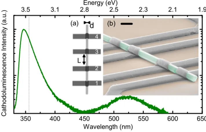
First, low temperature CL was used to structurally char-acterize the GaN material and evaluate the carrier concentra-tion. CL is produced by the radiative recombination of the excess electron hole pairs created during e-beam exposure. It is a suitable technique to probe microstructures, thanks to its nanometer resolution. Low temperature (10 K) CL spectra were taken with a 20 keV electron beam with spot size of 50 nm and current around 100 pA. A representative spectrum for the Si-doped GaN wires is reported in Figure 1. Near
FIG. 1. Low temperature (10 K) cathodoluminescence spectrum for a Si-doped GaN wire. Near-band edge for relaxed non-intentionally Si-doped bulk GaN (dashed line). Inset: (a) schematic view of a microwire in a four-probe configuration and (b) FESEM image of a connected microwire after comple-tion of the contacting process steps (scale bar 2lm).
a)
Electronic mail: [email protected]
b)Electronic mail: [email protected]
0003-6951/2013/102(12)/122116/4/$30.00 102, 122116-1 VC2013 American Institute of Physics
band edge (NBE) luminescence energy (E ! 3.57 eV) is revealed on the spectrum. The wire exhibits a weak defect-related band (“yellow band”) centered at 525 nm. The latter is generally assigned to gallium vacancies or oxygen com-plexes.8The asymmetric and broad NBE emission is blue-shifted compared to relaxed non-intentionally doped bulk GaN (E¼ 3.472 eV (Ref. 9)). The NBE peaks at 3.57 eV with full width at half maximum (FWHM) of 170 meV. This blue shift is consistent with band filling (Burstein Moss) effect resulting from high carrier concentration in the con-duction band and has been reported in the case of films10and recently GaN nanowires.11 Based on photoluminescence studies of peak position12 and FWHM13 in Si-doped GaN thin films, both the NBE peak position and the FWHM sug-gest carrier concentration above 1020 cm$3. The estimated carrier concentrations at 10 K are consistent with the observed metallic conduction (discussed later).
In the case of wire-shaped devices, one cannot easily access the important electrical transport parameters such as mobility and carrier concentration as generally measured by Hall measurements in thin films. Field-effect transistor is a helpful device generally used to evaluate the carrier concen-tration. However, it cannot be applied here due to the micro-scale of the wires and the too highly doped material. In any case, accuracy relies on the difficult estimation of the gate capacitance and interface charges. To strengthen the results from cathodoluminescence, resistivity measurements have, therefore, been performed. A specific e-beam lithography setup has been used to connect single microwires in a single-step electron beam lithography using CL mapping.14 First, wires were mechanically dispersed on 100 nm (thermally grown) SiO2/Si (p-type,q ¼ 1 X cm) and buried under 2
lm-thick PMMA resist. Then, wires were located under the resist using CL signal, and the resist was exposed according to the lithography pattern. Finally, evaporation of Ti/Al (60 nm/ 300 nm) and subsequent lift-off were carried out. Room tem-perature electrical measurements were performed using a standard probe station, whereas low temperature ones use a liquid helium stage and an electrical probing system setup inside a SEM.
Inset of Figure 1shows a field-emission scanning elec-tron microscope (FESEM) picture of a wire after completion of the process steps (b) and a sketch of the electrodes pattern to perform four-probe measurements (a). A current (I14) is
forced through the outer metallic electrodes (1 and 4) while the voltage drop between the inner electrodes (2 and 3) is measured. The resistivity q is then calculated using the equation
q ¼ V23=I14% S=L;
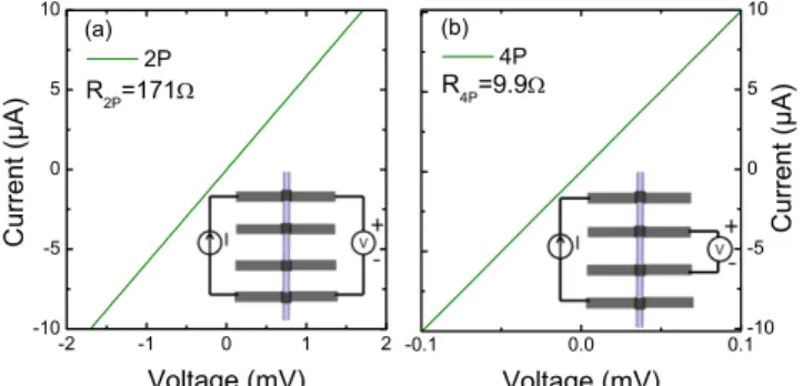
where L is the distance between the two inner electrodes and S¼ 3pffiffiffi3=2% ðd=2Þ2 is the section of a regular hexagon with side length d/2. Figure2shows the I-V characteristics in two-probe (2P) (a) and four-probe (4P) (b) configurations. The linear characteristics reveal the ohmic behavior of the contacts and the satisfactory contacting of microwires using standard electron-beam lithography techniques. Current den-sity was limited to 600 A/cm2to avoid Joule heating related effect. Reverse polarity measurements were performed to get rid of potential offsets.
Using the 4P configuration, measurements of eight wires yield resistivities in the range (0.37–0.75) mX cm. Figure
3(a) shows the room-temperature resistivity versus wire ra-dius. A nearly constant resistivity is observed for radii vary-ing between 650 nm and 1.3lm. This is consistent with a homogeneous radial carrier concentration within the wires where surface-related effects on conduction are negligible. Using a reported model for the Fermi-level pinning15 with value of surface potential barrier for air-exposed wires16 /B¼ 0:2 eV, one obtains a high estimation of the depletion
region close the surface. This value is found to be lower than 4 nm for Si-doped GaN wires assuming a carrier concentra-tion n¼ 1020 cm$3, in agreement with negligible surface
effects.17
Once the resistivity is known, one can deduce the resist-ance due to contacts Rc;i (i is the contact number) in a 2P
configuration assuming a symmetrical contact resistance (Rc¼ Rc;2¼ Rc;3) :R2P¼ q % L=S þ 2 % Rc.
Rccan be as high as 80X in comparison with wire
re-sistance (typically!10 X). Contrary to nanowires where the resistance obtained from 2P measurements could be a good approximation for the intrinsic wire resistance, 4P measure-ments are mandatory for conductive microwires. Using the method described by Mohneyet al.,18one can calculate spe-cific contact resistancesqc¼ Rc% ScwhereSc¼ 5/2 % d % w
is the contact area and w is the metal-microwire contact length. qc was found to be in the range (5) 10$6$ 10$5)
X cm2
. Specific contact resistances reported here are
FIG. 2. (a) Two-probe (2P) and (b) four-probe (4P) ohmic I-V characteris-tics of a Si-doped GaN microwire with diameter d¼ 1.72 lm and inner-electrodes distance L¼ 5 lm.
FIG. 3. (a) Room-temperature resistivity versus wire radius and (b) temperature-dependent resistivities for Si-doped GaN wires.
consistent with the literature on n-GaN films19 with (Ti/Al) metallization. The quality of our contacting technique is thus confirmed even on microscale devices and allows reliable 4P resistivity measurements.
Room-temperature resistivity measurements however do not provide information about the conduction regime occur-ring in a semiconductor. For this purpose, temperature-dependent resistivity measurements have been performed in order either to determine ionization energies or to evidence a metal-like conduction depending on the doping level. It is well known that the activation energy decreases with increasing silicon doping.20The latter has actually the effect to broaden the donor band D0from an isolated donor level
up to a degeneracy regime21where the carrier concentration is constant versus temperature. Experimental work for the metal-nonmetal transition gives doping density of NMNM
¼ 1:6 % 1018 cm$3.20
Figure 3(b) shows that the resistivity of the wires is not temperature dependent over the studied temperature range 10 K-300 K. The electrical conduction is therefore, purely metal-like with carrier concentration well above NMNM.
Due to the microscale of the studied wires, one can use the resistivity dependence on carrier concentration from GaN films in order to estimate the carrier concentration in the wires. The room temperature carrier concentration de-pendence of mobility in n-type GaN films has been reported in the literature. Chin et al.22 calculated electron mobility using a variational approach taking into account dominant scattering mechanisms (ionized impurity, piezoelectric, acoustic deformation potential, and polar-mode optical pho-non). Resistivityq can be deduced from calculated mobility l (Ref.22) usingq ¼ 1=ðl % q % n), where n is the electron carrier concentration and q is the electronic charge.
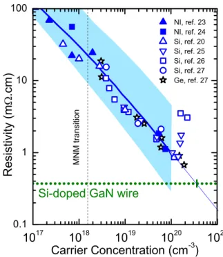
Resistivity versus carrier concentration for a range of compensation ratios K (defined as the acceptor concentration divided by the donor concentration) is illustrated by the blue area in Figure4. This blue area is limited by a bottom border (K¼ 0) and a top border (K ¼ 0.9) and illustrates the com-bined effect of compensation and doping on mobility. Experimental data for n-doping with different dopants (non-intentional, Si, Ge) are also reported. Figure4illustrates how the modeling with K¼ 0.6 (thick line) is consistent with ex-perimental data from the literature. Silicon doping (open symbols20,25–27) is shown to be effective for carrier concentra-tion up to n! 1020 cm$3 in decreasing the resistivity with the lowest resistivity value of 0.9 mX cm. However, for higher doping levels, self-compensation dominates26resulting in a drastic increase of K and a higher resistivity. Germanium-doped sample with n¼ 1:9 % 1020 cm$3 (star27) follows the modeling trend with K¼ 0.6.
Although it has been recently reported,28 direct mea-surement of the carrier concentration through Hall effect measurements are difficult on wires. In this work, resistivity for a Si-doped GaN wire is thus compared as a horizontal line in order to evaluate the carrier concentration in the wires. This graph allows one to gain a direct insight into the link between measured resistivity of samples and carrier concentration.
The resistivities measured here for Si-doped wires are lower than reported in Figure4 for other wurtzite n-doped
GaN material grown by MOVPE. In order to explain the high conductivity measured in Si-doped wires, one can first consider ideally no compensation (K¼ 0). Following this hypothesis, the lower bound in carrier concentration would be n¼ 8 %1019 cm$3for the wire reported in Figure4. Corresponding
mobilities would be larger than 200 cm2V$1s$1 (twice the
reported values in GaN films in Figure4). On the contrary, con-sidering K¼ 0.9 would lead to dopant incorporation above 1021 cm$3corresponding to an alloy Ga(Si)N.
The actual situation lies somewhere between these two extreme cases. The high conductivity in the Si-doped wires suggests, therefore, either an improved incorporation of sili-con atoms compared to bulk case and/or a higher mobility in GaN microwire in comparison to bulk material. However, the large wire diameter (more than 1lm) does not allow to consider any quantum improvement effect on the mobility. It is not straightforward either how compensation in heavily doped semiconductors could be weakened due to the micro-wire geometry. The real compensation ratio being between the two extrema, effective carrier concentration is more likely to be close to 4% 1020cm$3 assuming K¼ 0.6 and using Figure4.
An improved silicon incorporation in substitutional Ga site could then be responsible for the large carrier concentra-tion. Silicon incorporation in GaN films is well-controlled but limited to typical value of 5% 1019–1020 cm$3. For sili-con doping level larger than 2% 1019 cm$3, some cracks have been reported in wurtzite GaN29and the surface rough-ens on a micrometer scale in order to relax strain in the
FIG. 4. Room temperature resistivity as a function of electron concentration in n-doped GaN. Calculated resistivities22versus carrier concentration from
1017 cm$3to 1020 cm$3are reported by the blue area illustrating different
compensation levels K from 0 (bottom border) to 0.9 (top border). The thick solid line represents K¼ 0.6 for carrier concentration from 1017 cm$3to
1020 cm$3while the thin line is a guide to the eye linear extrapolation up to
1021 cm$3. Experimental resistivities are reported for films grown by
MOVPE with non intentional (NI),23,24 silicon,20,25–27 and germanium27 doping. Resistivity for the most conductive Si-doped GaN microwire is plot-ted as a horizontal line.
layer.27 On the contrary, Fritze et al.27 reported growth of Ge-doped GaN films (star in Figure 4) with n¼ 1:9 %1020 cm$3 and resistivities of 0.7 mX cm. They
demon-strated that incorporation of germanium was not resulting in additional stress in the layer, hence the ability to characterize electrically such highly doped material. In the case of wire growth, the use of heavily Si-doped GaN material is not hampered by the appearance of cracks. Additionally, the wire growth along [000"1] (N-polarity) should favor the incorporation of silicon dopants compared to growth along [0001] (Ga-polarity) as shown in Ref.12 on homoepitaxial GaN layers. This result points out the crucial role of polarity and supports the interest for research in this field.30
To summarize, carrier concentration in numerous Si-doped GaN microwires grown by catalyst-free MOVPE has been electrically investigated by 4P resistivity measurements and optically by cathodoluminescence. Single microwires are contacted and exhibit metal-like conduction without any temperature dependence between 10 K and 300 K. Measurements yield room-temperature resistivity never reported with values as low as 0.37 mX cm. Near band edge luminescence was found to be asymmetric and broad, with full width half maximum of 170 meV, suggesting band filling effect. From these two results, a carrier concentration around 4% 1020 cm$3 is likely to be achieved assuming a compen-sation ratio of 0.6. An improved silicon incorporation in GaN wires compared to film case is suggested to be responsi-ble for the high conductivity. The improved silicon incorpo-ration has been discussed in terms of N-polarity. Such a high conductivity demonstrates the interest of microwires and paves the way to more efficient current injection schemes and improved series resistances in wire-based devices.
The authors acknowledge G. Feuillet for fruitful discus-sions and the Nanofab team at Institut N!eel for the use of their facilities and their technical assistance. Research was partially supported by the French National Research Agency within the FIDEL Project (ANR-11-NANO-27).
1Y. Huang, X. Duan, Y. Cui, and C. M. Lieber, Nano Lett.
2, 101 (2002).
2
A. L. Bavencove, D. Salomon, M. Lafossas, B. Martin, A. Dussaigne, F. Levy, B. Andre, P. Ferret, C. Durand, J. Eymery, L. S. Dang, and P. Gilet,
Electron. Lett.47, 765 (2011).
3R. Koester, J. J.-S. Hwang, D. Salomon, X. Chen, C. Bougerol, J.-P.
Barnes, L. S. Dang, L. Rigutti, A. de Luna Bugallo, G. Jacopin, M. Tchernycheva, C. Durand, and J. Eymery, Nano Lett. 11, 4839–4845 (2011).
4
R. Calarco, M. Marso, T. Richter, A. I. Aykanat, R. Meijers, A. V. D. Hart, T. Stoica, and H. L€uth,Nano Lett.5, 981 (2005).
5F. Werner, F. Limbach, M. Carsten, C. Denker, J. Malindretos, and
A. Rizzi,Nano Lett.9, 1567 (2009).
6X. J. Chen, G. Perillat-Merceroz, D. Sam-Giao, C. Durand, and J. Eymery,
Appl. Phys. Lett.97, 151909 (2010).
7R. Koester, J. S. Hwang, C. Durand, L. S. Dang, and J. Eymery,
Nanotechnology21, 015602 (2010).
8L. Polenta, A. Castaldini, and A. Cavallini,J. Appl. Phys.
102, 063702 (2007).
9K. Kornitzer, T. Ebner, K. Thonke, R. Sauer, C. Kirchner, V. Schwegler,
M. Kamp, M. Leszczynski, I. Grzegory, and S. Porowski,Phys. Rev. B60, 1471 (1999).
10
B. Beaumont, G. Nataf, J. C. Guillaume, and C. V!eri!e,J. Appl. Phys.54, 5363 (1983).
11
E. Oh, B. W. Lee, S.-J. Shim, H.-J. Choi, B. H. Son, Y. H. Ahn, and L. S. Dang,Appl. Phys. Lett.100, 153110 (2012).
12P. Prystawko, M. Leszczynski, B. Beaumont, P. Gibart, E. Frayssinet, W.
Knap, P. Wisniewski, M. Bockowski, T. Suski, and S. Porowski,Phys. Status Solidi B210, 437 (1998).
13M. Leroux, B. Beaumont, N. Grandjean, P. Lorenzini, S. Haffouz, P.
Vennegues, J. Massies, and P. Gibart, Mater. Sci. Eng. B 50, 97 (1997).
14
F. Donatini and L. S. Dang,Nanotechnology21, 375303 (2010).
15
T. Richter, H. Luth, R. Meijers, R. Calarco, and M. Marso,Nano Lett.8, 3056 (2008).
16
M. Kocˇan, A. Rizzi, H. L€uth, S. Keller, and U. Mishra,Phys. Status Solidi B234, 773 (2002).
17
It must be noticed that the resistivity is determined assuming an homoge-neous carrier concentration (in both axial and radial directions) and con-duction through the entire wire section. In the case where a gradient exists, there will be regions in the wire with resistivity even lower than reported here.
18S. Mohney, Y. Wang, M. Cabassi, K. Lew, S. Dey, J. Redwing, and T.
Mayer,Solid-State Electron.49, 227 (2005).
19
M. E. Lin, Z. Ma, F. Y. Huang, Z. F. Fan, L. H. Allen, and H. Morko,
Appl. Phys. Lett.64, 1003 (1994).
20A. Wolos, Z. Wilamowski, M. Piersa, W. Strupinski, B. Lucznik, I.
Grzegory, and S. Porowski,Phys. Rev. B83, 165206 (2011).
21
A. Ghazali and J. Serre,Phys. Rev. Lett.48, 886 (1982).
22
V. W. L. Chin, T. L. Tansley, and T. Osotchan,J. Appl. Phys.75, 7365 (1994).
23M. Asif Khan, J. N. Kuznia, J. M. Van Hove, D. T. Olson, S.
Krishnankutty, and R. M. Kolbas,Appl. Phys. Lett.58, 526 (1991).
24
S. Strite,J. Vac. Sci. Technol. B10, 1237 (1992).
25X. Liu, L. Wang, D.-C. Lu, D. Wang, X. Wang, and L. Lin, J. Cryst.
Growth189–190, 287 (1998).
26
I. Halidou, Z. Benzarti, Z. Chine, T. Boufaden, and B. El Jani,
Microelectron. J.32, 137 (2001).
27
S. Fritze, A. Dadgar, H. Witte, M. B€ugler, A. Rohrbeck, J. Bl€asing, A. Hoffmann, and A. Krost,Appl. Phys. Lett.100, 122104 (2012).
28
K. Storm, F. Halvardsson, M. Heurlin, D. Lindgren, A. Gustafsson, P. M. Wu, B. Monemar, and L. Samuelson, Nat. Nanotechnol. 7, 718–722 (2012).
29
L. T. Romano, C. G. Van de Walle, J. W. Ager, W. G€otz, and R. S. Kern,
J. Appl. Phys.87, 7745 (2000).
30
S. Fern!andez-Garrido, X. Kong, T. Gotschke, R. Calarco, L. Geelhaar, A. Trampert, and O. Brandt,Nano Lett.12, 6119 (2012).