All-Optical Switching Using Semiconductor
Amplifiers Biased at Transparency
by
Bryan S. Robinson
Submitted to the Department of Electrical Engineering and Computer
Science
in partial fulfillment of the requirements for the degree of
Master of Engineering in Electrical Engineering and Computer Science
at the
MASSACHUSETTS INSTITUTE OF TECHNOLOGY
June 1998
( Bryan S. Robinson, MCMXCVIII. All rights reserved.
The author hereby grants to MIT permission to reproduce and
distribute publicly paper and electronic copies of this thesis document
in whole or in part, and to grant others the right to do so.
A
uthor
...
- . . ./...
Department of Electrical Engineering and Computer Science
May 13, 1998Certified by ... tN...
Hermann A. Haus
Institute Professor
",,ri*s Supervisor
Accepted
by
.
...
Arthur C. Smith
Chairman, Department Committee on Graduate Students
u
! ;
J
All-Optical Switching Using Semiconductor Amplifiers
Biased at Transparency
by
Bryan S. Robinson
Submitted to the Department of Electrical Engineering and Computer Science on May 13, 1998, in partial fulfillment of the
requirements for the degree of
Master of Engineering in Electrical Engineering and Computer Science
Abstract
In this thesis, we discuss how the nonlinear refractive index, linear and nonlinear loss, and dispersion of a waveguide affect interferometric all-optical switching devices. We perform simulations to demonstrate the detrimental effects of long-lived gain and refractive index changes in interferometric switches. The effects of long-lived index changes are reduced in a single arm interferometer, such as the ultrafast nonlinear interferometer. However, the effects of long-lived gain changes remain a problem. We suggest the use of semiconductor optical amplifiers biased at the transparency point as a means of reducing the long-lived effects of carrier population dynamics in semiconductor waveguides.
We demonstrate a spectral interferometric technique for measuring the nonlinear phase shift in optical pulses due to self-phase modulation in a nonlinear material. This technique, which has previously been used for dispersion measurements, is based on observation of the spectral interference of two temporally separated pulses before and after propagation through the nonlinear material. Using this technique, we measure the nonlinear phase shift induced in optical pulses propagating through semiconductor optical aplifiers biased at transparency. Our results suggest that switching at the transparency point is possible.
We use semiconductor optical amplifiers biased at the transparency point in var-ious switching demonstrations. We show the effects of long-lived gain changes as-sociated with carrier populations dynamics in the absorption and gain regime of a semiconductor waveguide. We show amplitude modulation in the output pulses of a switch arising from gain saturation. We demonstrate 10 Gbits/s all-optical switching using a semiconductor optical amplifier biased at the transparency current.
Research Supervisor: K. L. Hall Title: Senior Staff, Lincoln Laboratory Thesis Supervisor: Hermann A. Haus
Acknowledgments
It has been a great privilege to have Professor Haus as my thesis and academic advisor. His enthusiastic lectures in 6.013 are largely responsible for my decision to pursue a degree in electrical engineering. As an academic advisor, Professor Haus has shown a genuine interest in my success at MIT. In spite of his busy schedule, Professor Haus always made time for me when I needed it (usually on short notice).
I have really enjoyed working with Katie Hall at Lincoln Laboratory. I especially thank Katie for giving me the opportunity to work in her lab, despite my inexperience. She has been a great resource. Her technical knowledge is remarkable and her skills in the lab are unmatched. Whenever I was stumped, I knew she had a solution. I look forward to doing more work with Katie during the coming years.
I thank all the Lincoln staff members who generously offered advice and equip-ment for my research: Steve Chinn, Joe Donnelly, Jeff Korn, John Moores, Kristin Rauschenbach. Many students in the Advanced Networks group have made my ex-periences at Lincoln enjoyable: Victor Lum, Naimish Patel, Serena Chan, Tengo Saengudomlert, Dedric Carter, David Jones, and Erik Thoen. I am especially grate-ful for Claudia Fennelly and Kirk VanBrocklyn for keeping the labs organized and running smoothly, in spite of my best efforts.
Many friends at MIT have contributed to my success. Sara Ransom has been a constant source of support and motivation. I thank my roommate, Cayce Ramey, for his encouragement over the past four years. Thanks also to my friend, Jonathan Goldman, for general technical support and ISTFX advice. I am grateful for all my friends on the squash team and in the United Christian Fellowship for helping me keep my sanity throughout my time at MIT.
I have been blessed with a trully wonderful family. Thanks to Mom, Dad, Tom, Arnette for all the love and support. I hope you guys can share the joy that I have in finishing this work.
Finally, I thank God for changing my perspective at MIT and making this all possible.
Contents
1 Introduction 11
2 All-Optical Switching Background
2.1 Third-Order Nonlinearities ...
2.2 Nonlinear Mach-Zehnder Interferometer . 2.3 Mach-Zehnder Interferometer Problems 2.4 Ultrafast Nonlinear Interferometer . 2.5 Material Properties. 2.5.1 Nonlinearity. 2.5.2 Loss . . . . 2.5.3 Dispersion . . . . 2.5.4 Birefringence ... 3 Semiconductor Devices 3.1 Semiconductor Waveguides . 3.2 Carrier Population Dynamics 3.3 Nonlinear Gain Mechanisms . 3.4 Refractive Index ... 3.5 Dispersion ... 3.6 Discussion ... 3.6.1 Passive Devices . . 3.6.2 Transparency Point . 15 .. .. ... .. .. .. . . . .. 15 . . . 18 . . . 21 ... ... . .. .. ... . . .22 . . . 26 . . . 26 . . . 27 . . . 30 . . . 34 38 .. . 38 . .. 40 . .. .48 . .. . 51 .. . 55 * .. 56 . .. 57 . .. 58
4 Device Characterization
4.1 Measurement of Transparency 4.2 Spectral Interferometry . 4.3 Pulse Source .
4.4 Nonlinear Refractive Index . . 4.4.1 Other Effects. 4.5 Other Measurements. Current .. . . . .. .. I . . . . . . . 5 Switching Experiments 5.1 Experimental Setup . 5.2 Pulse Sources ... 5.2.1 Gain-switched Laser . . . . 5.2.2 PriTel Soliton Source.
5.2.3 Soliton Compression Source 5.3 Switching Results.
5.3.1 Interband Effects.
5.3.2 Patterning in Gain Regime . 5.3.3 Transparency ... 5.4 Discussion ... 6 Conclusions 6.1 Future Work . Bibliography 5 61 62 64 65 68 74 80 82 82 84 84 85 86 87 87 90 91 93 95 96 99
...
...
...
...
...
...
...
...
...
...
...
...
...
...
...
...
List of Figures
2-1 A Nonlinear Mach-Zehnder Interferometer ... 19
2-2 Output intensity versus total phase difference between the arms of a
nonlinear Mach-Zehnder interferometer ... 20
2-3 Simulation of effects of long-lived index changes in an unbalanced
in-terferometric all-optical switch ... 22
2-4 Block diagram of a single-arm interferometer. ... 23 2-5 Ultrafast-nonlinear interferometer implementation ... 23 2-6 Simulation of effects of long-lived index changes in an ultrafast
nonlin-ear interferometer. ... 24
2-7 Simulation of the effects of long-lived gain changes on the output pulses from the UNI. Here, the output is shown for the signal and control inputs shown in Figure 2-6 with carrier recovery times of 2.5 ps, 25 ps,
250 ps, and 2.5 ns. ... 25
2-8 Intensity required to achieve a r phase shift as a function of the
figure-of-merit, T . ... 30
2-9 Dispersion-induced broadening of a Gaussian pulse. ... 33 2-10 Inverse contrast ratio, R = Eoff/Eon of the UNI as a function of timing
offset of the two signal pulses normalized by the pulse width ... 36 2-11 Interference of two Gaussian pulses for various values of L/LD =
A/P2L/To2 where Ap32 = 32 - 2y. Initial Gaussian pulse width is
To. Initial intensitiy is Io. ... 37
2-12 Inverse contrast ratio of the UNI as a function of the difference in
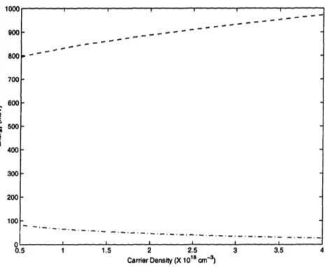
3-1 An index-guided semiconductor optical amplifier. ... 39 3-2 Dispersion relationship for a direct bandgap semiconductor. ... 40 3-3 The Fermi-Dirac distribution fuction for various temperatures .... 42 3-4 Quasi-Fermi energies as a function of the injected carrier density, N.
The dashed line is the quasi-Fermi energy for electrons in the conduc-tion band. The dot-dashed line is the quasi-Fermi energy for holes in
the valence band ... ... 44
3-5 Schematic of absorption process for a photon with energy hv ... 46 3-6 Gain coefficient, g, as a function of the excess photon energy, E - Eq. 4 8 3-7 Gain coefficient as a function of excess photon energy for various carrier
densities, N. The carrier densities are N x 10'8cm-3 = 0.7,1.8, and 3.0. 49 3-8 Gain coefficient as a function of excess photon energy for various carrier
temperatures. Here, the carrier temperature for the valence band is fixed at 300 K. The gain coefficient is shown for conduction carrier temperatures of 300 K (solid), 310 K (dashed), 320 K (dotted). .... 50 3-9 Changes in gain and refractive index due to carrier population density
changes. These changes correspond to carrier population changes of
AN(x 1018) = 0.02,0, -0.02, -0.05, -0.07 around N = 1.8 x 1018cm- 3. 53
3-10 Changes in refractive index for various gain changes, Ag(E), for carrier temperature changes of OK, +10K, +20K, +40K around 300K .... 54 3-11 Transparency wavelength as a function of the injected carrier
popula-tion density ... ... . 59
4-1 Experimental apparatus for measuring transparency current in a semi-condcutor laser amplifier. . . . ... 62 4-2 Measured differential voltage due to stimulated absorption and
emis-sion in a semiconductor optical amplifier as a function of the bias
cur-rent in the amplifier ... 63
4-3 Generic Mach-Zehnder Interferometer. ... 64
4-5 Spectrum from output port of stretched pulse laser. The solid line is the unfiltered output spectrum. The dashed line is the output spectrum
when a 4.93 nm filter is used. ... 67
4-6 Autocorrelation of a 640 fs pulse from the stretched-pulse laser with a
4.93 nm filter at the output ... 68
4-7 Method for measuring the nonlinear refractive index of a material using
spectral interferometry ... 69
4-8 Frequency domain interference for two Gaussian pulses. The FWHM for these pulses is 1 ps. The temporal spacing between the pulses is
T = 5 ps. The scaling factor is a = 0.25. ... 70 4-9 Frequency domain interference for two Gaussian pulses. The FWHM
for these pulses is 1 ps. The temporal spacing between the pulses is
T = 5 ps. The scaling factor is a = 0.25. The pump pulse has acquired
a uniform phase shift of r relative to the reference pulse. ... 72 4-10 Setup for creating two temporally separated pulses used in spectral
interferometry experiments. ... ... 73
4-11 Spectral interference and autocorrelation of two pulses used in
experi-ment ... .. 75
4-12 Measurements of phase shift in frequency domain versus average power
from pulse source ... 76
4-13 Spectral broadening due to self-phase modulation in a Gaussian pulse. 76 4-14 Spectral broadening due to self-phase modulation in a Gaussian pulse.
Here, the nonlinear refractive index change is assumed to have a
re-covery time of 600 fs ... 77
4-15 Simulation of interference of two Gaussian pulses. The pulse width is ips and the temporal separation is 5 ps. The scaling factor is a = 0.1. Interference patterns are plotted for peak phase shifts of 0, pi/2, and ir. 78 4-16 Simulation of observed phase shift in spectral modulation versus peak
phase shift due to self-phase modulation for two 1 ps Gaussian pulses. The pulses are separated by 5 ps and have scaling factor, a = 0.1. . . 79
4-17 Michelson interferometer used for directly observing the propagation
constant, /3(w) in a semiconductor optical amplifier ... 81 5-1 Experimental setup for swiching demonstrations. Optical paths are
indicated by solid lines. Electrical paths are indicated by dashed lines. 83 5-2 Autocorrelation of pulse from DFB laser modulated at 10 GHz before
and after compression in 400 m of dispersion compensating fiber. The FWHM is 32 ps before compression and 10 ps after compression . . . 85 5-3 Autocorrelation of 3.6 ps pulse from PriTel Soliton source operating at
12.5 GHz ... 86
5-4 Soliton compression source schematic. . . . ... 87 5-5 Autocorrelation of a 2 ps pulse from the 100 GHz soliton compression
source ... 88
5-6 Switching demonstration showing effects of carrier population changes
in various operation regimes ... 89
5-7 Amplitude modulatik. in the output signal due to gain suppression.. 90
List of Tables
3.1 Energy bandgap, and effective carrier masses for lattice-matched In-GaAsP/InP. mo is the effective mass of an electron in free space. .... 42 3.2 Group velocity dispersion measurements in InGaAsP semiconductor
Chapter
1
Introduction
In recent years, much research effort has been directed toward fully utilizing the information transmission capacity of optical fibers. Optical fibers transmit with low loss over a bandwidth of more than 200 nm. This corresponds to more than 25 THz of usable bandwidth for information transmission[2]. Taking advantage of this enormous capacity requires high-speed processing in network receivers and transmitters. For these types of simple processing applications, all-optical switches have a number of advantages over their electronic counterparts. For example, all-optical switches based on ultrafast nonlinearities can be used for switching at rates beyond 100 Gbits/s. All-optical- switches also have the advantage that signals may be propagated from one switch to another without upto-electronic conversion.
Ultrafast all-optical switches have many applications in the development of ultra-high speed multi-access time-division multiplexing (TDM) networks. For instance, bitwise logic is required in receivers in the network for tasks such as address recogni-tion, rate conversion, and demultiplexing [3]. All-optical switches can also be used for specific applications such as ultrafast data-encryption [4], analog-to-digital conversion [5], and wavelength conversion [6].
To date, many different switch designs have been proposed (for example, see [7]). These switches are often based on an interferometric design employing an intensity-dependent refractive index in a waveguide. A key design issue in an optical switch is the choice of nonlinear material. Numerous nonlinear materials have been employed
in optical switches to date.
The nonlinearities in optical fiber have been used in many all-optical switches [2]. The nonlinear response of optical fiber is composed primarily of bound-electron pro-cesses. The response time of these processes is virtually instantaneous with relaxation times that are typically less than 100 fs. This allows for switching at very high data rates. A nonlinear optical loop mirror using nonlinearities in fiber has been demon-strated for demultiplexing at rates up to 160 Gbits/s [8]. The main disadvantage of using optical fiber is that the nonlinear refractive index is very small. Thus, switching using fibers requires long interaction lengths (on the order of hundreds of meters) or high pulse intensities. Because very low loss fibers are available, these demands are not unreasonable. However, when using such long lengths of fiber, the accumulated effects of self-phase modulation and group velocity dispersion can lead to pulse dis-tortion [9, 10]. Pulse walk-through due to group-velocity dispersion can also reduce the effective length over which a signal pulse is affected by the fiber nonlinearity. In addition, long lengths of fiber make switches using optical fiber nonlinearities bulky and difficult to package.
As a result, semiconductor waveguides have become a very popular choice for nonlinear materials in all-optical switches. Semiconductors typically have a nonlinear refractive index that is more than four orders of magnitude larger than that of optical fibers. Hence, interaction lengths on the order of millimeters are suitable for obtaining a desirable phase shift. Semiconductors can also be reliably manufactured and easily integrated into a compact switch.
Logic gates employing nonlinearities in active semiconductors such as semicon-ductor optical amplifiers (SOA) have been demonstrated at rates up to 100 Gbits/s [11]. The SOA's in these switches are biased in the gain regime. Pulses propagating through these devices affect the carrier distributions within the semiconductor. The duration of these effects is governed by the carrier lifetimes of the device (typically > 100 ps). Consequently, gain saturation is observable at high data rates. The
re-sulting amplitude modulation in the output signal inhibits switching at higher rates
There are several alternatives to gain-biased SOA's which may avoid these com-plications without sacriiicig the convenience of using semiconductor waveguides for the nonlinear material. For instance, one may bias the semiconductor amplifier at the transparency point. At this point, net changes in the carrier populations of the device due to an incident optical pulse are eliminated. Thus, the nonlinear response of this material is potentially quite fast [12]. Recently, a low repetition rate, 2-ps switching window, was demonstrated in a switch using an amplifier biased at transparency [13].
Another approach is to use passive semiconductor waveguides. These waveguides are fabricated to have a bandgap energy slightly higher than the energies of the optical switching pulses. For these devices, at low optical pulse intensities, carrier populations remain relatively unchanged. Therefore, one expects a fast nonlinear response. Four wave mixing experiments in passive InGaAsP/InP semiconductors have confirmed the existence of a fast, relatively large, nonlinear refractive index in these devices [14].
In this thesis, we discuss methods for characterizing various nonlinear waveguides to determine their suitability for use in all-optical switches. A spectral interferometric technique is used to characterize the nonlinear refractive index in the devices. Suitable devices are demonstrated in all-optical switching experiments.
Chapter 2 presents background material on all-optical switching. We describe the operation of a nonlinear Mach-Zehnder interferometer, a common switch design used today. We discuss how third-order nonlinearities in optical materials can lead to a phase shift in an optical pulse traveling through the material. We describe the ultrafast nonlinear interferometer, the single-arm interferometer used for experiments in this thesis. We discuss the effects of non-instantaneous gain and index changes, loss, birefringence, and dispersion on all-optical switching in the UNI.
Chapter 3 contains a description of the semiconductor waveguides used in this the-sis. We begin with a discussion of the structure of active and passive semiconductor waveguides. A brief description of the carrier population dynamics of semiconductors is followed by a discussion of the third order nonlinearities of these devices. Re-suits of recent pump-probe studies of the nonlinear refractive index and dispersion
in semiconductors are presented. We discuss how passive waveguides and SOA bi-ased at transparency may be used to reduce the effects of long-lived gain changes in all-optical switches.
Chapter 4 describes the methods used for characterizing the nonlinearities in the semiconductor waveguides studied in this thesis. We show how observations of the interference between two optical pulses in the frequency domain allows direct obser-vation of the phase shift due to the nonlinear refractive index in a material. We use this spectral interferometric (SI) technique to measure the nonlinear refractive index in SOA biased at the transparency point. We discuss how SI may be used to measure dispersion and birefringence in waveguides.
Chapter 5 presents the results of various switching experiments performed using SOA's biased at transparency. We show the long-lived effects of gain changes in SOA's biased in the absorption and gain regimes. We demonstrate an all-optical AND gate operating at the transparency point. This is the first demonstration of ultrahigh speed all-optical switching in semiconductors biased at transparency.
Chapter 6 summarizes the results presented in this thesis. Suggestions for further study are presented.
Chapter 2
All-Optical Switching Background
In this section, I will present background material on the operation of all-optical switches. Most practical all-optical switches rely on a nonlinear phase shift accumu-lating in a signal pulse as it propagates through a nonlinear material. I will begin by discussing how such a phase shift arises due to third-order nonlinearities. Then, I will describe the basic operating principles of an interferometric switch. This is followed by a brief discussion of the ultrafast nonlinear interferometer (UNI), the all-optical switch used in this thesis. The chapter is concluded with remarks on how various material properities such as nonlinearity, loss, dispersion, and birefringence affect the operation of the UNI.2.1 Third-Order Nonlinearities
Third-order nonlinearities in an optical material can lead to an intensity dependent refractive index in the material. This nonlinear refractive index allows one to control the phase of a signal pulse using an intense control pulse. To better understand this interaction, we must consider the interaction of the two electric fields in the nonlinear material [15]. We write the signal pulse field as:
(t)
=
E + ) (21)where s is the carrier frequency of the pulse and Es(t) is the slowly-varying pulse envelope. For simplicity, we have assumed that the field is linearly polarized in the es direction. Similarly, we write the field of the control pulse as:
1
Ec(t) = c( Ec(t)e
- 3ct + c.c.).
(2.2)
The total field in the nonlinear material, E, is given by the sum of the signal and control fields.
In a third-order nonlinear material, a nonlinear polarization arises due to the interaction of the electric fields and the third-order nonlinear susceptibility tensor,
(3):.
pNL = EOX(3) :EEE (2.3)
Since the nonlinear susceptibility tensor is generally not instantaneous, the non-lineair polarization may be calculated by convolving the material impulse response, X(3)(tl, t2, t3) with the input field:
NL(3)
=
EJff
X(
3)(t - tl,t - t
2
,t - t
3)iE(t
1)E(t
2)E(t
3)dtldt
2dt
3.
(2.4) As a simple first approximation, let us assume that the signal and control pulses are copolarized in the x direction. Additionally, we shall assume that the nonlinear response of the material is instantaneous, X(3)(tl, t2, t3) = X(3)6(tl, t2, t3). The electric
field in the material may be written as: 1
E(t) = +k[(Es(t)eJws
t+ Ec(t)e-wc
t) ± c.c.].
(2.5)
2Substituting into equation 2.4 gives the nonlinear polarization [15]:
P()
=X{PPL(wS)e-js
+ PNL(c)e-jc
+ PNL(WS -2 W)e-j(2ws-w)t (2.6)
' PNL(
2C - ws)e
- j(2wc
-ws)t} + c.c.,
where
PNL(WS) = eff(IES 2+ 2jEc12)ES, (2.7)
PNL(WC) = Xeff(lEC2+ 2Es12)Ec, (2.8)
PNL(2WS - wc) = XeffEsEc, (2.9)
PNL(
2C
- WS) =
XeffECES,(2.10)
and the effective third order nonlinearity, Xeff = 3 'X3Z3)
We are interested in the change in the signal field due to the presence of the control field, so the relevant nonlinear polarization for our purposes is PNL(WS). We may rewrite the nonlinear contribution to the polarization as:
PNL(WS) = EOENLES (2.11)
where 6
NL = Xeff(lESI2 + 21EcI2). Thus, the total dielectric permittivity for the material is given by the sum of the linear and nonlinear parts[15]:
e = EL + ENL = (nL + An)2 (2.12)
where nL is the linear refractive index and An is the nonlinear contribution to the refractive index. If we assume An << nL we find:
where,
7n2 =: 83 Re(X3 (2.14)
Here, n2 is the so-called nonlinear refractive index coefficient. It is commonly used
to characterize the instantaneous nonlinear refractive index of a material.
From equation 2.13, we see that the index of refraction seen by the signal pulse is affected by both the intensity of the signal pulse and the intensity of the control pulse. The signal pulse therefore acquires a differential nonlinear phase shift as it propagates through a differential length dL:
d(nl = -r n2{lEsl2 + 2JEc 2}dL (2.15)
The contribution to the nonlinear phase shift from the signal pulse itself is known as self-phase modulation (SPM). The effects of SPM are discussed in more detail in Chapter 4. The contribution from the control pulse is known as cross-phase modula-tion (XPM). We shall show in the next secmodula-tion, (XPM) may be used in a nonlinear Mach-Zehnder interferometer to achieve all-optical switching.
2.2 Nonlinear Mach-Zehnder Interferometer
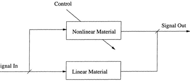
Many all-optical switch designs studied today are based on an interferometric ar-chitecture. A simple implementation of this design is the nonlinear Mach-Zehnder interferometer shown in Figure 2-1. Signal pulses with intensity in entering on the left are split into two pulses of equal intensity via a 50/50 beam splitter at the input. Pulses in the lower arm travel through a linear material with refractive index n = nt. Since the velocity of light traveling through this material is given by v = c/n, the phase change accumulated by the pulse while travelling through this material is given by:
Control
Signal In
Signal Out
Figure 2-1: A Nonlinear Mach-Zehnder Interferometer
where A is the freespace center wavelength of the optical pulse and L1 is the length
of the linear material.
Pulses in the upper arm travel through a nonlinear material. This material has an refractive index that is intensity dependent. That is, in the presence of an intense control pulse, the refractive index is given by: n = no +fn2Ic. The phase accumulated by the pulse as it propagates through this arm is given by:
>nonlinear L T(nt +- I n2lc)dz =- (n + n2Ic)Lnl (2.17)
where Ln1is the length of the nonlinear device.
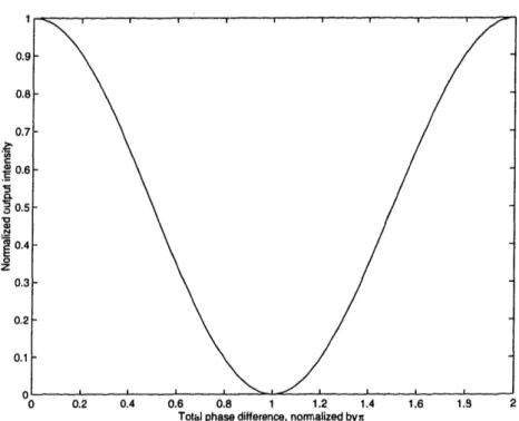
When the two pulses are interfered at the output, the output intensity is propor-tional to the relative phase shift in the two arms:
iout c I 11 + ei(liinear - nonlinear) 2
2
= I Cos2 (D Tbias -
)nl
2
Here, we have defined the bias phase shift, 4Dbias = 2, (nlL1 - n'Lnl1+ AL), where
AL is the difference in the freespace path lengths of the two arms. The bias phase
£.4 'S 0 a)1 z 0 0.2 0.4 0.6 0.8 1 1.2 1.4 1.6 1.9 z Total phase difference, nom',alized byn
Figure 2-2: Output intensity versus total phase difference between the arms of a nonlinear Mach-Zehnder interferometer.
lengths and linear refractive indices in the arms. Since the nonlinear phase shift term,
nl = - n2ICLn, (2.19)
is directly related to the intensity of the control pulse, we can control the output intensity of the signal pulses by adjusting the intensities of the control pulses. A plot of the output intensity as a function of the total phase difference between the arms is shown in Figure 2-2.
By appropriately setting the bias phase, we can switch the signal pulses ON or OFF using the control pulses. For instance, suppose that there is no bias phase, )bias = 0. Then, in the absence of a control pulse (Ic = 0), the signal pulse intensity at the output is equal to the signal pulse intensity at the input (neglecting losses in the system). If we introduce a control pulse into the second arm with sufficient intensity such that (nonlinear = 7r, the output signal pulses are completely switched
OFF (Iout = 0). In this case, the pulse energy has been redirected to the unused port on the output beam splitter. Alternatively, we can set the bias phase to r and use
the presence of a control pulse to switch the signal pulses ON, performing a logical AND function between the two pulse streams.
2.3 Mach-Zehnder Interferometer Problems
The nonlinear Mach-Zehnder interferometer described above, while attractive for its simplicity, is not a very practical design for an all-optical switch. Because signal pulses travel through separate paths in the interferometer, the switch may be imbalanced by thermal or acoustic variation between the two arms. These variations may affect the relative path lengths through which the signal pulses travel causing unintentional changes in the bias phase of the interferometer, (Ibias. This leads to unpredictable behavior from the switch. These problems can be reduced by using active path length stabilization. However, such a solution is generally difficult and unsatisfactory.
An additional problem with the nonlinear Mach-Zehnder interferometer arises when one considers that the response of the nonlinear material may not be instan-taneous. For example, semiconductor materials used in this thesis have nonlinear responses which have been observed to be well modeled by a sum of exponential decays with time responses ranging from a few femtoseconds to several nanoseconds [12]. If the refractive index changes from a single control pulse last more than one bit period, subsequent signal pulses may receive a nonlinear phase shift and be at least partially switched by the interferometer, even in the absence of a control pulse. These effects lead to undesirable patterning on the output pulses from the switch.
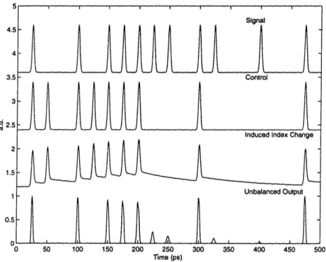
N. S. Patel has done simulations to demonstrate the effect of a long-lived nonlinear response in an unbalanced interferometer configured as an AND gate [16, 17]. In these simulations, the nonlinear phase response was assumed to have an instantaneous component, an ultrafast component with a relaxation time of 600 fs, and a long-lived component due to carrier with a relaxation time of 100 ps. The results of these simulations on a 40Gbps data stream are shown in Figure 2-3. The bits at the output suffer from amplitude modulation due to long-lived index changes. More significantly, output pulses are appearing in slots that should be zero. This reduces the contrast
0 50 100 150 200 250 300 350 400 450 500
Time (ps)
Figure 2-3: Simulation of effects of long-lived index changes in an unbalanced inter-ferometric all-optical switch.
ratio of the switch considerably.
2.4 Ultrafast Nonlinear Interferometer
Many of these problems can be remedied using a single-arm interferometer (SAI) switch design [18, 20]. The SAI works on the same principles as the nonlinear Mach-Zehnder interferometer, only signal pulses are separated temporally in a single arm. A block diagram of the SAI is shown in Figure 2-4. Signal pulses entering on the left are split into two equal-power, orthogonally-polarized pulses by a polarization sensitive delay (PSD). These pulses are separated by at least one pulse width. A copropagating control pulse is introduced after the PSD. This pulse is timed to overlap with precisely one of the signal pulses. All three pulses then travel through the nonlinear material
(NLM). Third order nonlinearities in the material cause a differential nonlinear phase shift in the overlapping signal pulse when a control pulse is present. The two signal pulses are then recombined temporally in a second PSD. Finally, the signal pulses are interfered in a polarizer and the control pulse is filtered out to give the output pulse.
Signal
Figure 2-4: Block diagram of a single-arm interferometer.
The ultrafast-nonlinear interferometer (UNI), shown in Figure 2-5, is a fiber im-plementation of the SAI. Entering signal pulses travel through a polarization sensitive isolator (PSI). At the output of the PSI, the signal pulses are linearly polarized at 45 degrees with respect to the fast and slow axes of a length of birefringent fiber (BRF) which acts as a polarization sensitive delay. After traversing the BRF, signal pulses pass through a 50/50 coupler where the control pulse is introduced. These pulses then travel through the nonlinear material (NLM). Signal pulses are temporally re-combined in a second length of BRF. The orthogonally polarized signal pulses are then interfered in a second PSI. Polarization paddles before the PSI allow adjustment of the bias phase of the interferometer. Finally, control pulses are filtered out using a fiber-coupled band-pass filter leaving the output signal pulse.
The UNI is a balanced interferometer. Both signal pulses in the UNI travel along the same path. So the problems encountered in the nonlinear Mach-Zehnder interfer-ometer due to thermal and acoustic variations between the two arms are eliminated. The UNI has been demonstrated at rates up to 100Gbps [11] with no active bias
stabilization.
The balanced interferometer design of the UNI also reduces the effects of
long-50/50 Coupler
Figure 2-5: Ultrafast-nonlinear interferometer implementation.
0 50 100 150 200 250 300 350 400 450 500
Time (ps)
Figure 2-6: Simulation of effects of long-lived index changes in an ultrafast nonlinear interferometer.
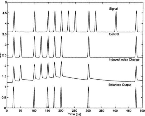
lived index changes. For example, if a control pulse induces a long-lived nonlinear refractive index change, subsequent signal pulse pairs sense these lingering changes equally and are not switched by the interferometer. Therefore, the UNI is insensitive to these long-lived index changes. Only ultrafast refractive index changes induced by a control pulse, introducing differential phase shifts between the two signal pulses, can cause the UNI to switch. N. S. Patel has performed other simulations of the effects of long-lived index changes in the UNI [16, 17]. The results of one these simulations are shown in Figure 2-6. This simulation used the same impulse response as the simulation of the unbalanced interferometer shown in Figure 2-3. The pulses in the UNI were temporally separated by 12.5ps. The effects of the long-lived index changes are negligible.
One reason the simulated results are so uniform is that they only take into account changes in the refractive index. There are also corresponding changes in the gain of the material. These gain changes may be related to the index changes through the Kramers-Kronig relations. In the UNI, gain changes that last more than one half of the bit period will be experienced by both signal pulses. We have performed
0 o 0. 0 z 0 t (ps)
Figure 2-7: Simulation of the effects of long-lived gain changes on the output pulses from the UNI. Here, the output is shown for the signal and control inputs shown in Figure 2-6 with carrier recovery times of 2.5 ps, 25 ps, 250 ps, and 2.5 ns.
simulations to show the effects of gain changes on signal pulses in the UNI using the analytical method described in [21]. For these simulations, we have used the same 40 GHz signal and control pulse patterns shown in Figure 2-6. We have assumed the energy in a single control pulse is 10 percent of the saturation energy for the nonlinear material and that the effects of the signal pulses are negligible compared to the effects of the high intensity control pulses. The small signal gain is assumed to be 20 dB. To isolate the gain effects, we have assumed that a uniform phase shift of r is obtained between the two orthogonal signal pulses when a control pulse is present. We have plotted the resulting output pulse stream for various values of the gain recovery time, Tc, in Figure 2-7. As is evident in the plot, when the gain recovery time becomes much longer than the bit period, significant patterning is observed on the output bits. This patterning limits achievable switching rates and prevents cascading of multiple switches.
2.5 Material Properties
In choosing a nonlinear material for use in the UNI, several characteristics of the material must be considered. The material must have a large, fast nonlinear response, low loss, small dispersion, and low birefringence. In this section, we discuss each of these properties and describe how they affect the operation of the UNI.
2.5.1 Nonlinearity
The ideal nonlinear material for an interferometric optical switch will have a very large third-order nonlinearity. As seen in Equation 2.19, the nonlinear phase shift induced in a signal pulse is directly related to the nonlinear refractive index, the in-tensity of the control pulse, and the length of the device. If n2 is small, large control
pulse intensities or device lengths are required to achieve a r phase shift. For ex-ample, optical fiber, a popular switching material has a relatively small nonlinearity (In21 3 x 10- 16 cm2/W). Optical switches have been demonstrated using fiber nonlinearities, but have required long lengths of fiber (100's of meters) to achieve reasonable switching intensities. Typically, one kilometer of fiber is needed to in-duce a 7r phase shift with peak pulse powers of 1 W. The third-order nonlinearity in semiconductor waveguides is typically 3-4 orders of magnitude larger than that of optical fiber. Additionally, because of the higher refractive index of semiconductors, the effective area of the guiding region in a single-mode semiconductor waveguide is typically smaller than the effective area of the core in an optical fiber. Thus, for the same optical power, optical intensities in a semiconductor waveguide are typically higher than they are in optical fibers. Hence, semiconductor device lengths on the order of a millimeter can be used for switching with reasonable signal intensities.
As we have already discussed, a fast third-order nonlinearity is desirable in ma-terials used in all-optical switches. However, many semiconductor mama-terials have a non-instantaneous third-order nonlinearity. The balanced interferometric design of the UNI reduces the effects of long-lived refractive index changes, but long-lived gain effects are still a problem. This is especially true in active semiconductor devices
where intense control pulses cause significant changes in the carrier populations. For example, when the device is biased for gain, above-band control pulses stimulate electron transitions from the conduction band into the valence band. These carrier-induced changes in the gain and refractive index may persist for tens of picoseconds to a few nanoseconds. Therefore, at high bit rates (> 10 Gbits/s) it takes several bit periods for these carriers to recover to their equilibrium state. This increases the linear loss of subsequent signal pulses and leads to undesirable amplitude modulation on the output.
In the past, most switching experiments using nonlinearities in semiconductors have been done with active devices biased in the gain regime (for example, [11, 22]). The problems with amplitude modulation were apparent in these demonstrations. Al-ternatively, one can use semiconductor optical amplifiers (SOA) biased at the trans-parency point or passive semiconductor waveguides. In SOA biased at transtrans-parency, the probability of a signal photon stimulating emission is equal to the probability of the photon stimulating absorption (see Chapter 3 for a more detailed discussion of transparency). A signal pulse travelling through the device causes no net changes in carrier populations. Thus, slow recovery times and gain dynamics are avoided. In passive waveguides, the signal and control wavelengths are below the bandgap of the material. Hence, linear absorption processes are nonexistent and carrier populations may remain relatively unchanged by low-power optical pulses propagating through the device. In both of these cases, however, ultrafast nonlineafities due to carrier heating, carrier scattering, and bound-electronic effects remain and may be utilized for all-optical switching. In this thesis, we will explore the properties of these devices in detail and determine their suitability for all-optical switching.
2.5.2
Loss
Consideration of waveguide losses is important since switching in the UNI is based on intensity dependent refractive index changes. In this section, we shall show that waveguide losses decrease the effective interaction length for signal and control pulses in the nonlinear material. This loss reduces the nonlinear phase shift accrued by the
signal pulses. As a result, higher control pulse intensities are required in waveguides with higher losses to achieve the desired phase shift. This necessitates the use of optical amplifiers and makes cascading of switches difficult.
The effect of losses on the pulse intensity, I(z), may be quantified as
= -a I-/312 +
(2.20)
Oz
The linear loss coefficient, ac, accounts for linear material losses, and linear absorption in materials. The nonlinear loss coefficient, f/, accounts for nonlinear losses such as two-photon absorption. In most cases p is quite small (on the order of 10 cm/GW in semiconductors), but its effects can become significant at high optical intensi-ties. Third-order and higher terms may be neglected for most practical applications. Equation 2.20 may be integrated to find the pulse intensity at a position z:
Io exp(-az)
I(z)
= 1 + o[ - exp(-az)]/a'
(2.21)
where Io is the intensity at z = 0.
In the limit of low nonlinear losses ( - 0), we have
1(z) = Io exp(-cz) (2.22)
Using this intensity profile, we find that the nonlinear phase shift induced in a signal pulse of wavelength A after propagating through a waveguide of length L with nonlin-ear refractive index n2 may be expressed as a function of the control pulse intensity,
I:
1
L2-
nI(z)dz
2r 1 - exp(-cL)\ (2.23)
-
2in2io (1- exp( L))
Note that this equation is identical to equation 2.19 if we define the effective interac-tion length Leff = [1 - exp(-aL)]/a. As ac becomes larger, the effective interaction
length approaches 1/a asymptotically. However, in this case, the losses are so large that switching is impractical.
Nonlinear losses also affect switching requirements. Including the effects of
/3,
we find that the nonlinear phase shift accrued over a length L is:(nl
=T
n2In + Io (1
- exp(-caL))(2.24)
To explore the individual effects of , set a = 0. Then, the nonlinear phase shift is
2ir 1
) = -nl 7 n2 In [1 + Io,3L]. (2.25)
We see that the initial intensity required to achieve a phase shift of 7r is
=f
3 L [exp1
n2) (2.26)In the absence of nonlinear losses (p = 0),
I°r= 2L (2.27)
2n2L'
Now, we find from equation 2.26,
I, exp(T) - 1
(2.28)
where
T= 3A (2.29)
2n2
The parameter T has been suggested as a figure of merit for switching using materials with nonlinear losses [23, 24]. Figure 2-8 shows the relationship between I/I ° and
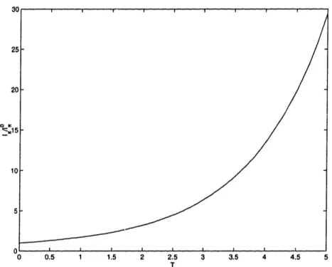
T. As T increases, the required control pulse intensities increase dramatically. To
0 0.5 1 1.5 2 2.5 3 3.5 4 4.5 5
T
Figure 2-8: Intensity required to achieve a r phase shift as a function of the figure-of-merit, T.
2.5.3 Dispersion
Dispersion in the nonlinear material also affects the operation of the UNI. In a dis-persive material, the propagation constant, , is a function of the frequency of light.
A short optical pulse contains many optical frequencies. In a dispersive waveguide, some of these frequencies propagate faster than others. This leads to pulse distortion as the faster frequencies move ahead of the slower frequencies.
Let us consider the effect of dispersion on a Gaussian pulse as an example. We write the propagation constant in the dispersive medium around a frequency wo as
1
$(w) =
3+ p3 (w
-)+
2,/3
2(w
-Wo)2+ . .,
(2.30)
where
fn
= , [25]. Now consider an initially unchirped Gaussian pulse with center frequency wo propagating in the z direction in the medium. We write theelectric field for the pulse at z = 0 as:
E(z = O, t) = Eoexp
-
2 exp(ijwot) (2.31)This pulse has a full-width at half-maximum (FWHM) of:
TFWHM = 2(ln 2) /2To (2.32)
The frequency content of the pulse is found by computing the Fourier transform of E(z = 0, t):
E(z = O,w) =
1 00 O, t) exp(-jwt)dtEoTo
r _7r
(2.33) exp ( (w - w) 2T2
Thus, the spectral content of the pulse is Gaussian, as well. The spectral FWHM is found to be:
2(ln 2)1/2
AWFWHM T
To
(2.34)
After propagating a distance L into the dispersive medium, the pulse spectrum becomes:
E(z = L, w) = E(z = O, w) exp (-j(w)L)
- EoTo
--
exp
2
2)(
°
- jlL( - o) -joL].
Note that the spectrum is still Gaussian with the same FWHM. However, there is now a frequency dependent phase shift in the spectrum, 4((z = L, w) = (w)L. Taking
the inverse Fourier transform of E(z = L, w), we find the time-domain equation for (2.35)
the pulse at z = L:
E(z = L, t) =
f
E(z = L, w) exp(jwt)dwEo exp [-j3oL - jwot] exp -2(To + L)
1
+
___,62L)xp
2(T&'
+ j
2
L)
(2.36)
The pulse is still Gaussian, although its shape has changed slightly. At this point, it is useful to define a few terms related to the frequency dependent propagation constant. The phase velocity of the pulse, vO= wo/3o, relates the speed at which the sinusoidal carrier frequency of the pulse is propagating through the material. Similarly, the group velocity, Vg = 1/,i, is the speed at which the pulse envelope is propagating through the material. Finally, 2 is the group velocity dispersion which relates to the rate at which the pulse is broadening in the dispersive r.edium. Defining the dispersion length, LD = To2/I32
l,
the pulse width at z = L is found to be [15]:TFWHM(Z = L) = 2(n 2)'12T0 1 + (L/LD) 2. (2.37)
The peak intensity is similarly found to be:
Ppeak 1 + (L/L) 2 (2.38)
Figure 2-9 shows the dispersion of a Gaussian pulse for various values of L/LD. This pulse distortion in the nonlinear material has important consequences for all-optical switching in the UNI. For materials with fast nonlinearities, the effect of the nonlinearity is reduced as the instantaneous peak intensity of the pulse lessens due to dispersion. The dispersion-induced reduction in peak intensity reduces the effective length of the nonlinear interaction between signal and control pulses. For slower nonlinear responses, this reduction in the peak intensity of the pulse is less of an issue as the effect of the nonlinearity is integrated over the entire pulse. That is, the nonlinearity is proportional to the pulse energy rather than the peak power.
A.
T/Tr
Figure 2-9: Dispersion-induced broadening of a Gaussian pulse.
that the signal pulses be separated temporally to isolate the nonlinear effects of the control pulse within the interferometer. If the control pulses become very wide, they may overlap both of the temporally separated signal pulses, reducing the differential effects of the nonlinearity in the interferometer and making switching difficult. Signal pulses are also affected by dispersion. In the extreme case, signal pulses may become so broad that they interfere with neighboring pulses. While this problem may not arise in a single switch, it may become a significant issue when cascading of multi-ple switches is considered. Hence, choosing a material with a small group velocity dispersion, P2, relative to the length of the device is important.
The problems associated with dispersion are a primary reason for using semicon-ductor waveguides for the nonlinear material in all-optical switches instead of optical fiber. Long lengths of fiber are required to achieve a 7r phase shift with reason-able pulse energies. This means that dispersion is a significant issue when fiber is used. Indeed, in these lengths of fiber, other issues such as pulse walk-through due to the different group velocities of signal and control pulses arise. Since semiconductor waveguides can achieve the same phase shift in a device that is less than a millimeter
in length, the effects of dispersion are reduced.
2.5.4
Birefringence
Birefringence occurs when the propagation constant for a material, (w) is
polariza-tion dependent. In ordinary optical fiber and bulk semiconductor waveguides, this effect is typically negligible. Some of the semiconductors tested in this thesis contain
quantum wells, however. In these quantum wells, the lattice structure of the
semicon-ductor is strained, inducing birefringence in the device. This birefringence affects the ope. ation of the UNI since the two signal pulses propagating through the nonlinear material have orthogonal polarizations. Different propagation constants between the two polarizations will affect the interference of the pulses at the output.
Suppose that the propagation constant for the x polarization is 3x(w) and the propagation constant for the y polarization is y(w). Then, define the difference between these two propagation constants
Ap(w) = PX(w) - fy(w)
(2.39)
= +A
0+ P
1(W
- wO)
+ ..
2(.
-WO)
2+
Each of the constants, A,3o, Aill, and A32, has a different affect on the operation of the UNI which must be considered.
The modal birefringence, l0, relates the difference in the phase velocities of the two polarizations. From equation 2.36, we see that this difference results in an overall phase difference between the two pulses. This phase contributes to the bias phase of the interferometer. The initial phase bias of the UNI is important because it determines its logical operation. However, the changes in bias phase due to modal birefringence can be easily compensated by adjusting the polarization paddles prior to the polarizer at the output of the switch.
A more serious problem arises when there is a difference in group velocities, ZAf. This is also referred to as the polarization mode dispersion (PMD). Birefringent fiber, for instance, typically has a PMD of - 1.5 ps/m [26]. When PMD exists in the UNI,
the two orthogonally polarized signal pulse envelopes propagate at different speeds. After propagating through a device of length L, the two envelopes will be offset by a time T- = A,31L. Hence, they may not overlap at the output. This reduced overlap
may affect the contrast ratio of the switch. To observe this effect, consider a Gaussian pulse at the input of the UNI,
E(t)
=Eoexp -2
exp(-jwot).
(2.40)
Suppose the UNI imparts d uniform r phase shift on one of the signal pulses in the nonlinear material. Additionally, suppose that the difference in the group velocities of the pulses in the material delays one of the signal pulse envelopes by time r. Then, the intensity of the pulse at the output of the interferometer will be:
Iout(t)
or E(t)
E(t - -r)
2 (2.41)Integrating this intensity with respect to time gives the energy of the pulse. Figure 2-10 shows the inverse contrast ratio of the UNI, defined as the energy of the switched OFF pulse divided by the energy of the switched ON pulse, as a function of /To. Note that a small inverse contrast ratio is desired for optimum switching performance. As the inverse contrast ratio approaches 1. it becomes more difficult to distinguish the ON pulse from the OFF pulses.' As r increases, we observe that the ability of the UNI to switch OFF pulses lessens. Differences in the group velocities of the signal pulses may be compensated for by adjusting the length of the polarization sensitive delays (PSD) in the UNI. However, this would only fix the problem for a single nonlinear material with signals at a particular wavelength. If the material or signal wavelength were changed later, one would have to recalibrate the length of the PSD accordingly. Clearly this is not a very desirable solution.
Differences in the group velocity dispersions of the two polarizations, A/P2 also affect the operation of the UNI. Such a difference leads to the signal pulses having different widths and intensities when they are interfered at the output of the UNI. This
C 'I I o re Ln W -5 -4 -3 -2 -1 0 1 2 3 4 5 Time offset r/To
Figure 2-10: Inverse contrast ratio, R = Eoff/Eo,, of the UNI as a function of timing offset of the two signal pulses normalized by the pulse width.
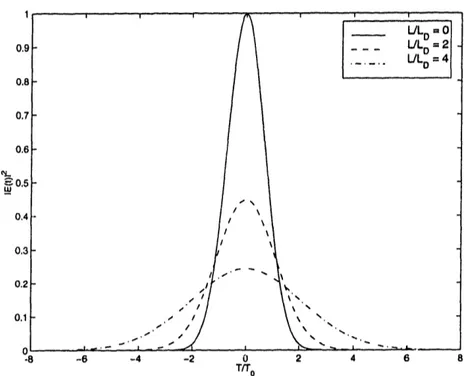
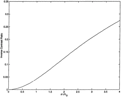
leads to nonuniform interference at the output. Figure 2-11 illustrates the effect of nonuniform interference on the output pulse shape. Here, one of the pulses experiences no dispersion and propagates through the device undistorted. The second pulse has a uniform r phase shift relative to the first pulse and experiences dispersion as it propagates through the device. The figure shows the interference of the two pulses for various dispersion lengths, LILD. When no dispersion occurs (LILD = 0), the output pulse is completely switched OFF, as expected. As the dispersion increases, the output is no longer completely switched OFF. When LILD = 4, the peak output pulse intensity is almost half of the original pulse intensity. Figure 2-12 shows a the inverse contrast ratio of the UNI as a function of the difference in GVD for the two polarizations.
C
S
Ai
-8 -6 -4 -2 0 2 4 6 8
Time VT
Figure 2-11: Interference of two Gaussian pulses for various values of L/LD =
A/ 2L/T 2 where A/32 = 2x - 32y. Initial Gaussian pulse width is To. Initial
in-tensitiy is Io.
0
a)
A LD
Figure 2-12: Inverse contrast ratio of the UNI as a function of the difference in dispersion, AL/LD = 32L/To2 where A/32 = p/2 -32y.
Chapter 3
Semiconductor Devices
In this chapter, we will describe the semiconductor waveguides used in this thesis. We begin with a description of a typical semiconductor waveguide. This is followed by a discussion of the carrier population dynamics in semiconductors. We describe how these interactions lead to linear gain. Then, we present the various mechanisms which cause nonlinear gain changes in semiconductor waveguides. Next, we show how the nonlinear gain changes of a semiconductor relate to nonlinear refractive index changes through a Kramers-Kronig transformation. Then, we discuss measurements of dis-persion in semiconductor waveguides. Finally, we discuss the use of semiconductors in all-optical switching.
3.1 Semiconductor Waveguides
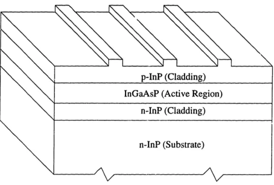
A typical index-guided semiconductor waveguide like those studied in this thesis is shown in Figure 3-1 [27]. The;device is a dielectric waveguide consisting of a layer of InGaAsP (the active region) between two layers of InP (the cladding regions). The higher refractive index of the InGaAsP region confines light in the vertical direction. The ridge etched in the top layer of InP provides an effective index change which confines light in the horizontal direction.
The device pictured is a diode, or p-n junction. When the diode is forward biased, carriers are injected into the active region of the waveguide. The bandgap of the
Figure 3-1: An index-guided semiconductor optical amplifier.
InGaAsP layer is engineered to be less than that of the surrounding InP laters. This potential barrier created by the layers serves to confine the injected carriers to the active region where most optical interactions occur. Such as device is commonly referred to as "active." A passive waveguide has a similar structure, only the cladding regions are not necesarily doped to create a p-n junction, and carriers are not injected electrically into the material.
The facets of the semiconductor waveguide are typically cleaved normal to the waveguide. However, since the refractive index of the semiconductor is relatively large, the reflectivity of these facets is quite high (typically - 0.3). This large reflectivity of the end facets causes coupling losses and creates Fabry-Perot cavity effects. For example, in an active device, these mirrors provide feedback and may enable laser activity. To reduce these effects, the facets may be cleaved at an angle or anti-reflection (AR) coated. In this case, the waveguide provides gain, but lasing is not achieved. Such a device is called a semiconductor optical amplifier (SOA).
E
n Band
k
Valence Band
I•
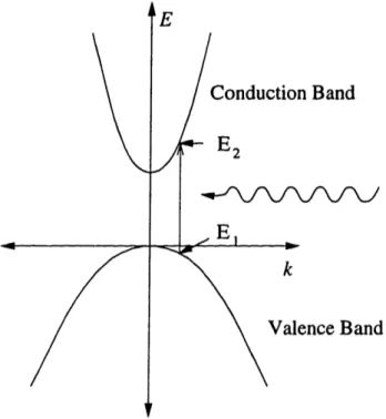
Figure 3-2: Dispersion relationship for a direct bandgap semiconductor.
3.2 Carrier Population Dynamics
Optical interactions with semiconductors are strongly influenced by carrier population dynamics within the semiconductor. Electrons in a semiconductor are distributed among the avaliable energy levels of the semiconductor. The highest filled energy level in a direct bandgap semiconductor at OK is known as the valence band. The
conduction band is separated from the valence band by an energy bandgap, Eg. No
electrons reside in the energy levels between the valence and conduction bands. In semiconductors, Eg is on the order of a few eV. Electrons in the valence band may be excited into the conduction band. These, excited electrons, known as free carriers, fill the bottom of the conduction band, leaving behind holes in the top of the valence
band.
Near the bottom of the conduction band, the band structure of a typical semicon-ductor is well approximated by a parabola [28]. If we define the top of the valence band as having 0 energy, the energy in the conduction band as a function of the wave
vector k is given by:
h2k2
EC(k) = Eg + 2m (3.1)
Here, me is the effective mass of electrons in the conduction band and k is the mag-nitude of k. Similarly, the energy structure in the valence band may be written as:
h2k2
E (k)
=-
2(3.2)
mh
where mh is the effective hole mass in the valence band. Figure 3-2 shows an example dispersion relation for electrons in a direct bandgap semiconductor. It is interesting to note the similarity between these dispersion equations and the dispersion relationship for a free electron. Indeed, negative-charged electrons in the conduction band and positive-charged holes in the valence act much like free carriers with masses me and
mh, respectively. Their movement in response to an applied voltage gives rise to current.
The devices studied in this thesis are fabricated using the quaternary semicon-ductor Inl_.GaAsyPl_,. The InGaAsP is grown on an InP substrate. In or-der to ensure that these two semiconductors are lattice matched, we must have
x = 0.4526y/(l - 0.031y) [29]. The energy bandgap and effective masses for
elec-trons in the conduction band and holes in the valence band in lattice-matched In-GaAsP/InP are given in Table 3.1 Note that the bandgap can be varied between 0.75eV and 1.35eV (0.92/Lm < AG < 1..65/um). This region of energies overlaps with the low loss energies in optical fiber, making InGaAsP devices very practical choices for integration in fiber-optic data networks.
Electrons in a semiconductor are subject to the Pauli-exclusion principle. This dictates that at most two electrons (with opposite spin states) can occupy the same energy state simultaneously. The distribution of electrons among the available energy states at thermal equilibrium is thus described by Fermi-Dirac statistics. The prob-ability that an electron occupies a state with energy E is given by the Fermi-Dirac
Parameter Value
Energy bandgap Eg = 1.35 - 0.72y + 0.12y2
Eff. electron mass me/mo = 0.080 - 0.039y
Eff. hole mass mh/mo = (1 - y)[0.79x + 0.45(1 - x)] + y[0.45x + 0.4(1 - x)]
Table 3.1: Energy bandgap, and effective carrier masses for lattice-matched In-GaAsP/InP. mo is the effective mass of an electron in free space.
\, \ N. I 0 0.2 0.4 0.6 0.8 1 E/EF T =0 T> 0
\\
I' \ \'. \ '\ \ 'x 1.2 1.4 1.6 1.8Figure 3-3: The Fermi-Dirac distribution fuction for various temperatures. distribution function:
1
fe(E) = e(E-EF)/kBT + 1
Here, T is temperature and kB is Boltzmann's constant. The energy EF is known as the Fermi energy. At the Fermi energy, the probability of occupation is precisely 1/2. The Fermi-Dirac distribution fuction is plotted in Figure 3-3 for several temperatures. When T = 0 the distribution is simply a step function with all states below the Fermi energy filled. As T increases, thermal energy excites electrons into higher energy states, smearing out the distribution and filling the conduction band.
When the semiconductor is not in thermal equilibrium, the distribution of
elec-0.9 0.8 0.7 0.6 -- 0.5 0.4 0.3 0.2 0.1 - .- = . L . ,,. , , . ... l 1 \ ____ ~ -- r, t I I
trons in the valence band and the conduction band cannot be written in terms of a
single Fermi energy. Minority carrier injection into the bands is one way that the thermal equilibrium may be disturbed. If the number of injected carriers is small, the distribution of electrons within a particular band may remain in equilibrium among themselves. In this case, the quasi-Fermi energies for the valence and conduction bands are distinct. We write these energies as EFt and EFV, respectively. The distri-bution of electrons is then:
1
f(E) e(E-EFc)/kBT + 1
in the conduction band, and
1
fd(E)
= e(E-EF)/kBT + 1in the valence band.
The density of states in the valence band, p(E), is defined so that p(E)dE quantifies the number of available energy states in the range (E, E + dE) for a semiconductor[28]. The number of states in a region of k-space enclosed by a spherical shell of thickness dk is:
1
nk = (2 47rk2dk. (3.6)
(27)3
Now, if we use the parabolic approximation for the dispersion relation between E and
k, we find for the valence band,
p (E)
=
r{2mh)
3/ (-E)1/2 (3.7)Similarly we find that the density of states in the conduction band is given by