Publisher’s version / Version de l'éditeur:
Applied Physics Letters, 90, 4, 2007-01-01
READ THESE TERMS AND CONDITIONS CAREFULLY BEFORE USING THIS WEBSITE. https://nrc-publications.canada.ca/eng/copyright
Vous avez des questions? Nous pouvons vous aider. Pour communiquer directement avec un auteur, consultez la
première page de la revue dans laquelle son article a été publié afin de trouver ses coordonnées. Si vous n’arrivez pas à les repérer, communiquez avec nous à PublicationsArchive-ArchivesPublications@nrc-cnrc.gc.ca.
Questions? Contact the NRC Publications Archive team at
PublicationsArchive-ArchivesPublications@nrc-cnrc.gc.ca. If you wish to email the authors directly, please see the first page of the publication for their contact information.
NRC Publications Archive
Archives des publications du CNRC
This publication could be one of several versions: author’s original, accepted manuscript or the publisher’s version. / La version de cette publication peut être l’une des suivantes : la version prépublication de l’auteur, la version acceptée du manuscrit ou la version de l’éditeur.
For the publisher’s version, please access the DOI link below./ Pour consulter la version de l’éditeur, utilisez le lien DOI ci-dessous.
https://doi.org/10.1063/1.2390652
Access and use of this website and the material on it are subject to the Terms and Conditions set forth at
Large Area 50 nm Period Grating by Multiple Nanoimprint Lithography
and Spatial Frequency Doubling
Cui, Bo; Yu, Zhaoning; Ge, Haixiong; Chyou, Stephen Y.
https://publications-cnrc.canada.ca/fra/droits
L’accès à ce site Web et l’utilisation de son contenu sont assujettis aux conditions présentées dans le site LISEZ CES CONDITIONS ATTENTIVEMENT AVANT D’UTILISER CE SITE WEB.
NRC Publications Record / Notice d'Archives des publications de CNRC:
https://nrc-publications.canada.ca/eng/view/object/?id=f1101659-6367-4ee6-ae6f-4100fbc55b7e https://publications-cnrc.canada.ca/fra/voir/objet/?id=f1101659-6367-4ee6-ae6f-4100fbc55b7e
Large area 50 nm period grating by multiple nanoimprint lithography
and spatial frequency doubling
Bo Cui, Zhaoning Yu, Haixiong Ge, and Stephen Y. Choua兲
NanoStructure Laboratory, Department of Electrical Engineering, Princeton University, Princeton, New Jersey 08544
共Received 15 August 2006; accepted 5 October 2006; published online 25 January 2007兲
The authors have developed an approach to fabricate large area 50 nm period gratings 共22 nm linewidth兲 with low cost. The method used a fabrication cycle twice, each combining nanoimprint lithography with a spatial frequency doubling based on electroless plating, lift-off, and reactive ion etching. Hence by frequency doubling twice, we started with a 200 nm period grating mold and finished with a 50 nm period grating with a uniform area of 3 cm2—the largest achieved today. This method is scalable for the fabrication of even smaller period gratings over a large area, and is a viable low-cost technique for making nanoimprint lithography molds for high-throughput fabrication of 50 nm period grating or grid devices. © 2007 American Institute of Physics. 关DOI:10.1063/1.2390652兴
Large area sub-200-nm period grating or grid structures have many applications, such as in deep-ultraviolet polarizers1and transmission or reflection filters,2,3broadband antireflection surfaces where the grating linewidth 共or grid pillar diameter兲 increases gradually with depth,4high density patterned magnetic data storage media5 or nonvolatile mag-netoresistive random access memory,6 nanofluidic channels to stretch, align, or sort genomic DNA,7array of field emit-ters for flat-panel display,8 and atom beam or x-ray diffraction.9,10They are also used for fundamental research.
Previous fabrication methods for sub-200-nm grating in-clude electron-beam lithography, electron holographic lithography,11 and extreme ultraviolet interferometry.12,13 However, besides being expensive, they all have limited field size and low throughput, and are difficult to extend to large areas. Achromatic interferometric lithography14is capable of producing large area 100 nm period gratings with high throughput, yet it is complex in tools and processes, and has not generated gratings of 50 nm period or smaller.
An alternative fabrication technique that can relax the lithography requirement is the “frequency doubling,” which doubles the number of lines of a grating fabricated by other methods.15–18 A frequency doubling has been reported for fabricating large area 100 nm period grating from a 200 nm period grating.19 However, the frequency doubling process can be lengthy, hence reducing the yield and increasing the cost. In this letter, we present an approach to double the grating frequency. Compared with previous frequency dou-bling method, the present one offers far better control of grating periodicity because of two innovations: 共a兲 the use of electroless plating to precisely control the line/gap width 关us-ing feedback from scann关us-ing electron microscopy 共SEM兲 measurements, one can easily adjust the line/gap width by removing plated materials and replating兴 and 共b兲 the use of nanoimprint lithography 共NIL兲 关which has shown pattern du-plication of 6 nm half pitch20兴 to achieve high fidelity and high-yield pattern duplication for multiple frequency dou-bling. The frequency doubling process was carried out twice
to achieve a 50 nm period grating from a 200 nm period grating.
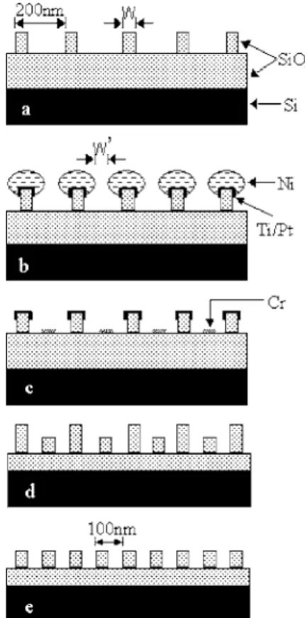
The details of the frequency doubling procedure are shown in Fig. 1. For making a 100 nm period grating, we started with a 200 nm period grating in SiO2 grown on 4 in.
Si wafer, generated by interference lithography or nanoim-print lithography. The grating was duplicated in the SiO2
layer of another Si wafer using NIL, lift-off, and reactive ion etching 共RIE兲. Then the 200 nm period grating lines were narrowed by HF wet etch to a width W, which is about half
a兲
Author to whom correspondence should be addressed; electronic mail: chou@princeton.edu
FIG. 1. Schematic of 100 nm period grating fabrication by spatial frequency doubling: 共a兲 200 nm period grating with narrow line by NIL; 共b兲 Ti/ Pt catalyst layer deposition and electroless Ni plating; 共c兲 Cr evaporation and lift-off by Ni in nitric acid; 共d兲 SiO2RIE and metal wet-etch removal; 共e兲
planarization by polymer spun-on and etch-back. APPLIED PHYSICS LETTERS 90, 043118 共2007兲
0003-6951/2007/90共4兲/043118/3/$23.00 90, 043118-1 © 2007 American Institute of Physics
of the final grating period 共50 nm in this case兲. Next, a thin Ti/ Pt 共adhesion/catalyst, total 3 nm兲 layer was angle evapo-rated from both sides of the grating to cover the upper part of the SiO2 line. Ni was deposited electrolessly at a rate of
30 nm/ min, which formed “mushrooms” on the grating line. The size of the mushroom was controlled so that the gap between the mushrooms, W
⬘
, is equal to W. With the assis-tance of SEM measurements, we have achieved near identi-cal W and W⬘
共within 5 nm兲. Thirdly, 10 nm Cr was evapo-rated at an incident angle normal to the wafer. The openings between adjacent mushrooms allowed the Cr to be deposited onto the bottom of the SiO2 trenches. Then Ni mushroomswere dissolved in diluted nitric acid 共Ti/ Pt not attacked兲 to lift off the Cr deposited on top of the mushroom. The Cr in SiO2 trenches interdigited with the original SiO2 grating to
form a new grating with half of the original period 共doubled frequency兲. The Cr grating and SiO2grating 共will be etched兲
served as a RIE mask in a CHF3/ O2 RIE to transfer the
pattern into the underneath SiO2. Then Cr, Ti, and Pt were
wet etched away using commercial Cr photomask etchant, 1:100 diluted HF 共etched negligible oxide兲, and hot HNO3: HCl: H2O = 1 : 7 : 10, respectively. Finally, the wafer
surface was planarized by the conventional polymer spun-on and plasma etch-back technique. The polymer was customer developed in house that could achieve the same RIE etching rate as SiO2by adjusting the partial gas pressure of O2and
CHF3. The polymer was completely removed by O2plasma
afterward.
The electroless plating solution formulation is shown in TableI. Both thickness uniformity and line edge smoothness are critical for the frequency doubling process. The plated Ni was found to be smooth. To achieve uniform deposition, the electroless plating must start simultaneously everywhere, and the deposition rate should be constant across the wafer. We chose dimethyl amine borane 共DMAB兲 as reducing agent because, with the same substrate preparation procedure, we found that the plating was easier to start simultaneously with DMAB than with other reducing agents. As for the deposi-tion rate, electroless plating 共as a chemical process兲 is intrin-sically much more uniform than electrical plating, especially when the deposition rate is limited by chemical reaction rate. Figure2 shows film thickness uniformity over 4 in. silicon wafer coated with Ti/ Pt. The plating was performed in an ultrasonic tank for improving film uniformity and a fast re-moval of generated H2 gas to eliminate pinholes. The film
thickness was within a 5% variation on area within 4 cm from the wafer center, but became thicker on the wafer edge. This indicates that mass diffusion rate, determined by reac-tant concentration and solution agitation, still played an im-portant role in determining the plating rate. By attaching the
sample to a larger sacrificial wafer, one can reduce the edge effect considerably.
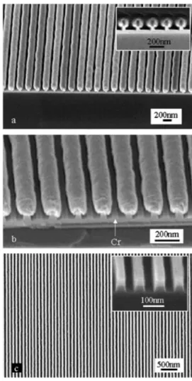
Figure 3 shows the fabricated 100 nm period grating from a 200 nm period NIL mold together with SEM images after two intermediate steps. Electroless Ni plating onto the 200 nm period grating is shown in Fig.3共a兲. As expected, the electroless Ni covered only the upper part of the grating lines where Ti/ Pt were coated, forming a mushroom profile. Cr was then evaporated onto this grating at normal incident angle. SEM image 关Fig. 3共b兲兴 shows that the Cr on trench bottom was disconnected from the Cr on top of Ni; hence the subsequent Cr lift-off in nitric acid was straightforward. Fig-ure 3共c兲 shows the completed 100 nm period grating with TABLE I. Electroless Ni plating solution formulation. It has been diluted to
40% that of designed strength to reduce the plating rate for better deposition control. NiSO2· 6H2O 16 g / l Na citrate 10 g / l DMAB 0.2 g / l Thiourea 0.8 mg/ l pH 共NH4OH兲 8.5 Temperature 65 ° C Boron in deposit ⬍0.7%
Plating rate ⬃30 nm/ min FIG. 2. Electroless Ni film uniformity over 4 in. Si wafer coated with Ti/ Pt. Thickness is measured by AFM.
FIG. 3. Fabrication of 100 nm period grating. 共a兲 SEM image after electro-less Ni plating. The inset shows the sideview, 共b兲 after Cr evaporation at normal incident angle, and 共c兲 the completed 100 nm period grating with 55 nm linewidth. The inset shows the cross section.
043118-2 Cui et al. Appl. Phys. Lett. 90, 043118 共2007兲
linewidth of 55 nm. The new set of grating lines could not be distinguished from the old set. The surface topology after planarization was measured by atomic force microscopy 共AFM兲 and showed a fluctuation of ⬍5 nm, which is small enough for the grating to be used as a NIL mold. The edges of each line appear a little rough due to the line edge rough-ness of the original 200 nm period master mold. The uniform area, defined here by 5 nm linewidth difference between the two sets of lines, and limited by the linewidth nonuniformity of the master mold, is ⬃10 cm2.
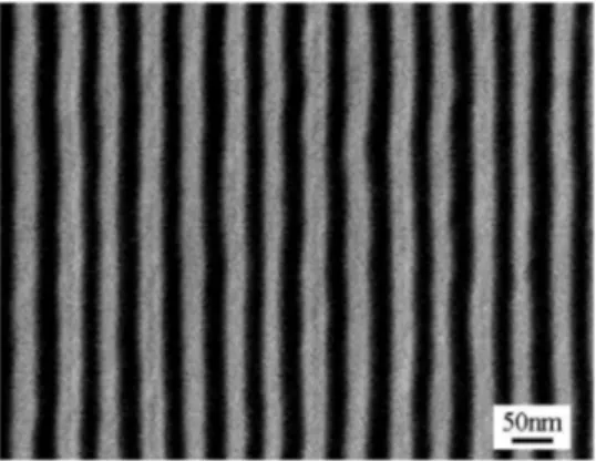
After having the 100 nm period grating, we used it to carry out another cycle of nanoimprint and frequency dou-bling process to achieve a 50 nm period grating. The com-pleted 50 nm period grating with about 22 nm linewidth is shown in Fig.4. The line roughness and irregularity of the master 200 nm period grating are further amplified in the 50 nm period case. The uniform area, due to process error and master grating nonuniformity, is reduced to about 3 cm2.
With better process control, the 50 nm period grating could have a uniform area over 10 cm2.
The current fabrication process involves only NIL, elec-troless plating, metal evaporation and lift-off, and RIE, which are all low-cost processes. In addition, unlike interfer-ence lithography, this process is scalable for even smaller
period gratings. Combined with NIL, one would find a num-ber of applications, particularly in the field of patterned mag-netic recording media or subwavelength optical devices.
This work was supported in part by ONR and DARPA. 1
E. E. Scime, E. A. Anderson, D. J. McComas, and M. L. Schattenburg, Appl. Opt. 34, 648 共1995兲.
2
M. Gruntman, Appl. Opt. 34, 5732 共1995兲.
3
T. M. van Beek, R. C. Fleming, P. S. Hindle, J. D. Prentiss, M. L. Schattenburg, and R. Ritzau, J. Vac. Sci. Technol. B 16, 3911 共1998兲.
4
Y. Ono, Y. Kimura, Y. Ohta, and N. Nishidan, Appl. Opt. 26, 1142 共1987兲.
5
S. Y. Chou, M. S. Wei, P. R. Krauss, and P. B. Fischer, J. Appl. Phys. 76, 6673 共1994兲; B. Cui, W. Wu, L. Kong, X. Sun, and S. Y. Chou, ibid. 85, 5534 共1999兲.
6
B. Vogeli, H. I. Smith, F. J. Castano, S. Haratani, Y. W. Hao, and C. A. Ross, J. Vac. Sci. Technol. B 19, 2753 共2001兲.
7
R. H. Austin, J. O. Tegenfeldt, H. Cao, S. Y. Chou, and E. C. Cox, IEEE Trans. Nanotechnol. 1, 12 共2002兲.
8
C. O. Bozler, C. T. Harris, S. Rabe, D. D. Rathman, M. A. Hollis, and H. I. Smith, J. Vac. Sci. Technol. B 12, 629 共1994兲.
9
R. E. Grisenti, W. Schöllkopf, J. P. Toennies, J. R. Manson, T. A. Savas, and H. I. Smith, Phys. Rev. A 61, 033608 共2000兲.
10
D. Hambach, G. Schneider, and E. M. Gullikson, Opt. Lett. 26, 1200 共2001兲.
11
K. Ogai, Y. Kirmura, R. Shimizu, J. Fujita, and S. Matsui, Appl. Phys. Lett. 66, 1560 共1995兲.
12
M. G. Capeluto, G. Vaschenko, M. Grisham, M. C. Marconi, S. Ludueña, L. Pietrasanta, Y. Lu, B. Parkinson, and C. S. Menoni, IEEE Trans. Nano-technol. 5, 3 共2006兲.
13
H. H. Solak, D. He, W. Li, S. S. Gasson, S. S. Cerrina, B. H. Sohn, X. M. Yang, and P. Nealey, Appl. Phys. Lett. 75, 2328 共1999兲.
14
T. A. Savas, M. L. Schattenburg, J. M. Carter, and H. I. Smith, J. Vac. Sci. Technol. B 14, 4167 共1996兲.
15
D. C. Flanders and N. N. Efremow, J. Vac. Sci. Technol. B 1, 1105 共1983兲.
16
L. F. Johnson and K. A. Ingersoll, Appl. Phys. Lett. 38, 532 共1981兲.
17
G. J. Sonek, D. K. Wagner, and J. M. Ballantyne, J. Vac. Sci. Technol. 19, 921 共1981兲.
18
D. C. Flanders and A. E. White, J. Vac. Sci. Technol. 19, 892 共1981兲.
19
Z. Yu, W. Wu, L. Chen, and S. Y. Chou, J. Vac. Sci. Technol. B 19, 2816 共2001兲.
20
M. D. Austin, H. Ge, W. Wu, M. Li, Z. Yu, D. Wasserman, S. A. Lyon, and S. Y. Chou, Appl. Phys. Lett. 84, 5299 共2004兲; M. D. Austin, W. Zhang, H. Ge, D. Wasserman, S. A. Lyon, and S. Y. Chou, Nanotechnology 16, 1058 共2005兲.
FIG. 4. 50 nm period grating with 22 nm linewidth over a large area fabri-cated by doubling twice from a 200 nm period grating.
043118-3 Cui et al. Appl. Phys. Lett. 90, 043118 共2007兲