Vol. 119 (2011) ACTA PHYSICA POLONICA A No. 2
Proceedings of the 14th International Symposium Ultrafast Phenomena in Semiconductors, Vilnius 2010
Voltage Controlled Terahertz Transmission Enhancement
through GaN Quantum Wells
T. Laurent
a,∗, R. Sharma
a, J. Torres
a, P. Nouvel
a, S. Blin
a, L. Chusseau
a,
C. Palermo
a, L. Varani
a, Y. Cordier
b, M. Chmielowska
b, J.-P. Faurie
c,
B. Beaumont
c, P. Shiktorov
d, E. Starikov
dand V. Gruzinskis
daInstitut d’Electronique du Sud, UMR 5214 — CNRS/Université Montpellier 2
Pl. E. Bataillon, 34095 Montpellier, France
bCentre de Recherche sur l’Hétéro-Epitaxie et ses Applications, UPR 10 — CNRS
R. Bernard Grégory, 06560 Valbonne, France
cLUMILOG, 2720, Ch. Saint Bernard Les Moulins I, 06220 Vallauris, France dSemiconductor Physics Institute, A. Gostauto 11, 2600 Vilnius, Lithuania
We report transmission measurements of GaN quantum well grown on sapphire substrate in the 220–325 GHz frequency band at low temperatures. A significant enhancement of the transmitted beam intensity with the applied voltage on the devices under test is found.
PACS: 78.20.–e, 78.67.De, 73.21.Fg
1. Introduction
In the last years, there has been a growing interest in using the terahertz (THz) radiations as a powerful tool to investigate materials/devices/structures in chem-istry, biology, physics, medicine and materials science [1]. Consequently, a significant effort has been devoted to the study and development of solid-state sources of tun-able THz radiations. Indeed, the THz domain repre-sents a border range of frequencies between microwaves and infrared where intrinsic scientific and technological difficulties appear, leading to several approaches in the realization of THz sources. In the low-frequency part of the THz domain (i.e. f 6 100 GHz), generation is usually obtained either by starting from various current instabilities appearing in Gunn-, IMPATT-, Schottky--diodes etc. [2], which are then placed in a waveguide resonant cavity or by the mixing of CW or pulsed in-frared lasers [3–5]. From the high-frequency side (i.e. f > 5 THz), generation is usually achieved by optical methods making use of the stimulated radiation coming from quantum cascade lasers [6–9], p-Ge lasers [10, 11] or gas lasers [12] etc. In each of these ways, the generation efficiency decreases significantly when trying to extend
∗corresponding author; e-mail:
the generation into the central part of the THz region (i.e. 100 GHz 6 f 6 5 THz) [13]. Therefore, to develop new and efficient THz sources, it becomes mandatory to investigate new solid-state structures able to amplify the THz radiation leading to efficient power generation in this frequency range.
In this letter we present experimental results showing the possibility to control the intensity of THz radiations transversally transmitted through GaN-quantum wells at room and cryogenic temperatures by applying a dc volt-age in the longitudinal direction.
2. Samples under study
As far as the fabrication process of the GaN devices is concerned, the different layers consist of a sapphire substrate, a GaN iron doped template, a GaN 1 µm thick buffer, a 1 nm AlN/21 nm Al0.28Ga0.72N/3 nm
GaN active layer covered with Ti/Al ohmic contacts (see Fig. 1a). The Schrödinger–Poisson simulations were per-formed to evaluate the total concentration of electrons as well as the concentration on the first energy sub-band in the 2D-channel of the designed structure (see Fig. 1c). Results are summarized in Tables I and II for 10 and 300 K temperatures, respectively. The layers are grown and processed as described in [14]. The devices are not passivated. An ohmic contact resistance of 1–3 W mm is obtained depending on the sample. Capacitance volt-age and Hall measurements attest the presence of a
108 T. Laurent et al. -dimensional electron gas (2DEG) with a carrier
concen-tration of 1013cm−2 (very near to the theoretical value)
and a mobility of 2000 cm2/(V s). Since the area needed
to couple THz waves with the device under test (DUT) has to be in accordance with the wavelength (≈ 1 mm in our study), the choice have been made to use inter-digitated fingers structure for the contacts, with a length between contacts of the order of 19 and 39 µm and a to-tal width of 500 µm, as sketched in Fig. 1b. A scanning electron microscopy (SEM) picture of a sample is shown in Fig. 2.
Fig. 1. Vertical structure of the studied samples (a), contacts’ pattern (b), and conduction band diagram (c). The distances between contacts are 39 and 19 µm in the longest and smallest zones, respectively. The horizontal lines of (c) correspond to the three first energy levels of the heterolayer.
Fig. 2. Large view of interdigitated fingers obtained by SEM studies.
3. Experimental setup
A scheme of the experimental configuration can be seen in Fig. 3. A commercial electronic source generates con-tinuous harmonic waves in the 220–325 GHz frequency range. The beam is focused in a He-free cryostat by a first spherical mirror. With the help of the simulation of Gaussian beams propagation in this particular frequency domain, we estimated the position of the source needed
TABLE I Calculated fundamental and first excited energy levels measured with respect to the Fermi level in the GaN quantum well at 10 K together with the corresponding carrier density and the percentage of carrier population on each sub-band.
Magnitude E1 E2
energy −116 meV −19.6 meV
carrier density 9.87 × 1012cm−2 1.65 × 1012cm−2
ratio 85.6% 14.3%
TABLE II Calculated fundamental and first excited energy levels measured with respect to the Fermi level in the GaN quantum well at 300 K together with the corresponding carrier density and the percentage of carrier population on each sub-band.
Magnitude E1 E2
energy −107 meV −2.15 meV
carrier density 9.14 × 1012cm−2 1.60 × 1012cm−2
ratio 79.7% 13.9%
to obtain the waist in the center of the cryostat where devices under investigation (DUT) are maintained. The transmitted beam through DUT is then extracted from the cryostat and focused with the help of a second spher-ical mirror on a Si-bolometer. A lock-in amplifier system is used to extract the part of the bolometer signal corre-sponding to the transmitted beam. The frequency band investigated is limited by the electronic source we are using (220–325 GHz). The frequency resolution as well as the reproducibility are limited by the resolution and reproducibility of the frequency synthesizer. The elec-tric field is applied with the help of a continuous source--meter able to generate voltages from 0 up to 15 V, while the cryostat cold plate temperatures can be maintained at 300, 77, and 7 K.
Fig. 3. Experimental configuration for measurements of transmission spectra in the THz frequency domain.
It is thus possible, with such an experiment, to measure the effect of different conditions such as biasing condi-tions, temperature or geometrical parameters of the DUT on the transmission spectrum.
Voltage Controlled Terahertz Transmission Enhancement . . . 109 The experimental protocol is the following: first the
DUT is placed into the cryostat at the position defined by the Gaussian beams simulation, and then thermalized. When the desired temperature is obtained, the passive transmission of the bench without an applied dc bias to the DUT is measured. Then the same transmission spec-trum is acquired applying a dc bias.
4. Results and discussion
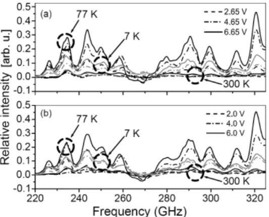
Several experiments have led to investigate the effect of different conditions such as frequency, electric field, and temperature on the transmission spectra of the GaN quantum wells. The main results are summarized in Fig. 4a and b showing the difference between the trans-mission spectra with and without bias (i.e. the relative in-tensity) as a function of the frequency for two DUT of 39 and 44 µm lengths respectively and for 7 K (top black), 77 K (gray) and room temperature (bottom black). The applied voltages of investigation vary between 0 and 7 V which correspond to average electric fields from 0 up to 1.5 kV/cm. From these results it is clearly shown that, at both 7 K and 77 K, the relative intensity is strongly de-pendent on the applied voltage whereas at room tempera-ture the signal exhibits only a weak dependence. Indeed, concerning the electric field dependence of the transmit-ted beam, we found that either at 77 or 7 K, the overall transmission intensity increases with the increase of the bias. If one looks closer, he would find that this pre-viously described enhancement is frequency dependent with an absorption of the beam that occurs for all stud-ied DUT near the 270 GHz frequency. The superimposed oscillations are mainly due to the used of the electronic source and do not reflect physical phenomena occurring inside the DUT such as interferences phenomenon.
Fig. 4. Subtraction of transmitted power — measured by Si-bolometer — with and without bias as a function of frequency, for two distances between contacts equal to 39 (a) and 44 µm (b) respectively, for three different biases and three different temperatures: from top to bottom, black corresponds to 77 K, gray to 7 K and bottom black to 300 K.
Focusing to the dependence with the temperature; as the electron mobility increases while the temperature is
decreasing, the intensity of the measured signal at room temperature is negligible in regard with the results ob-tained at cryogenic temperatures. Moreover, in opposi-tion to expected results, the enhancement of the intensity of the transmitted spectra is smaller at 7 K than at 77 K (Fig. 4). Indeed, at the lowest temperatures the electron mobility should improve the amplification. Two exper-imental reasons may explain this behavior. (i) For the 77 K measurements, the samples are directly cooled by a flow of liquid nitrogen into the cryostat whereas at 7 K the cryostat is cooled by a cryocooler system (helium cryogenic head and an associated compressor) and then by a flow of liquid helium into the vessel of the cryo-stat. The cryocooler system is running during all the ex-periment long and generates many mechanical vibrations on table where the focusing spherical mirrors are main-tained (Fig. 3). As a consequence, some misalignment of the incident beam may occur and globally involve a loss of power compared to measurements at other tempera-tures. (ii) From a physical point of view, one can involve the cooling of the sample at 7 K to explain the observed behavior. Indeed, cooling the DUT at 7 K may produce sample deformations that alter the electron transport, and as a consequence the electron mobility, through the contact and consequently decrease the transmitted THz signal intensity.
Fig. 5. Normalized to maximum transmitted power as a function of the applied bias for different frequencies for a 39 µm long device at 77 K.
Figure 5 shows for different frequencies, between 230 and 325 GHz, the evolution of the normalized transmit-ted spectra as a function of the applied bias at 77 K. Overall, the trend of the curves is to increase with the applied bias. In other words, this means that there is a positive effect of the applied bias on the transmitted power which may result in an amplification of the THz signal from the DUT. The real gain calculation of our devices is still pending and will be the object of an other publication. One can also see that there is, for the par-ticular frequency of 262 GHz, a “bell shape” dependence. Even if these experimental results have to be improved, specially regarding the frequency band studied in this letter, this dependence could be related to the optical phonon transit time resonance (OPTTR) phenomenon described in Ref. [15].
110 T. Laurent et al. 5. Conclusion
An original experimental configuration has allowed measurements of the transmitted THz signal intensity enhancement through specifically designed GaN 2-DEG. This enhancement can be controlled by the applied dc voltage. At the frequency of 262 GHz, a bell shape characteristic of the THz intensity versus applied volt-age allows to attribute this enhancement to the OPTTR phenomenon. If the amplification inside our devices is confirmed for a larger frequency domain, they could be considered as a part of an amplification system, which will provide efficient power amplification/generation into the THz frequency range.
Acknowledgments
The French National Research Agency (ANR) and the Lithuanian Science Council are sincerely acknowledged for funding the research work under contract AITHER no. ANR-07-BLAN-0321 and grant no. MIP-87/2010. This work was partially supported by GIS 053713 Tera-Lab Montpellier.
References
[1] D. Dragoman, M. Dragoman, Prog. Quant. Electron. 28, 1 (2004).
[2] G. Gallerane, S. Biedron, in: Proc. 2004 FEL Conf., Eds. R. Bakker, L. Giannessi, M. Marsi, R. Walker, Comitato Conferenze Elettra, Trieste 2004, p. 216.
[3] B. Ferguson, X. Zhang, Nature Mater. 1, 26 (2002). [4] N. Chimot, J. Mangeney, L. Joulaud, P. Crozat,
H. Bernas, K. Blary, J.F. Lampin, Appl. Phys. Lett. 87, 193510 (2005).
[5] J. Mangeney, L. Joulaud, P. Crozat, J.-M. Lourtioz, J. De-Cobert, Appl. Phys. Lett. 83, 5551 (2003). [6] J. Faist, F. Capasso, D.L. Sivco, C. Sirtori,
A.L. Hutchinson, A.Y. Cho, Science 264, 553 (1994). [7] R. Köler, A. Tredicucci, F. Beltram, H. Beere, E.H. Linfield, A. Davies, D. Ritchie, R. Iotti, F. Rossi,
Nature 417, 156 (2002).
[8] G. 8, C. Walther, J. Faist, H. Beere, D. Ritchie, Appl.
Phys. Lett. 88, 141102 (2006).
[9] B.S. Williams, S. Kumar, H. Callebaut, H. Qing, J.L. Reno, Appl. Phys. Lett. 83, 5142 (2003). [10] E. Brundermann, D. Chamberlin, E. Hallier, Infrared
Phys. Technol. 40, 141 (1999).
[11] M.A. Odnoblyudov, A.A. Prokofiev, I.N. Yassievich, K.A. Chao, Phys. Rev. B 70, 115209 (2004). [12] A. 12, H. Gebbie, M. Kimmitt, L. Mathias, Nature
201, 250 (1964).
[13] M. Tonouchi, Nature Photon. 1, 97 (2007).
[14] Y. Cordier, M. Azize, N. Baron, S. Chenot, O. Tot-tereau, J. Massies, J. Cryst. Growth 309, 1 (2007). [15] E. Starikov, P. Shiktorov, V. Gružinskis, L. Reggiani,
L. Varani, J.C. Vaissière, J.H. Zhao, J. Appl. Phys. 89, 1161 (2001).