HAL Id: hal-03184763
https://hal.archives-ouvertes.fr/hal-03184763
Submitted on 29 Mar 2021
HAL is a multi-disciplinary open access
archive for the deposit and dissemination of
sci-entific research documents, whether they are
pub-lished or not. The documents may come from
teaching and research institutions in France or
abroad, or from public or private research centers.
L’archive ouverte pluridisciplinaire HAL, est
destinée au dépôt et à la diffusion de documents
scientifiques de niveau recherche, publiés ou non,
émanant des établissements d’enseignement et de
recherche français ou étrangers, des laboratoires
publics ou privés.
Laura Monge-Bartolome, Bei Shi, Billy Lai, Guilhem Boissier, Laurent
Cerutti, Jean-Baptiste Rodriguez, Kei Lau, Eric Tournié
To cite this version:
Laura Monge-Bartolome, Bei Shi, Billy Lai, Guilhem Boissier, Laurent Cerutti, et al.. GaSb-based
laser diodes grown on MOCVD GaAsonSi templates. Optics Express, Optical Society of America
-OSA Publishing, 2021, 29 (7), pp.11268-11276. �10.1364/oe.419396�. �hal-03184763�
GaSb-based laser diodes grown on MOCVD
GaAs-on-Si templates
L
AURAM
ONGE-B
ARTOLOME,
1B
EIS
HI,
2B
ILLYL
AI,
2G
UILHEMB
OISSIER,
1L
AURENTC
ERUTTI,
1J
EAN-B
APTISTER
ODRIGUEZ,
1K
EIM
AYL
AU,
2 ANDE
RICT
OURNIÉ1,*1IES, Univ. Montpellier, CNRS, F-34000 Montpellier, France
2Department of Electronic and Computer Engineering, Hong Kong University of Science and Technology,
Clear Water Bay, Kowloon, Hong Kong
Abstract: We report GaSb-based laser diodes (LDs) grown on on-axis (001) Si substrates and emitting at 2.3 µm. Two series of LDs were studied and compared. For the first series, a GaAs-based buffer layer was first grown by metal organic chemical vapor deposition (MOCVD) before growing the laser heterostructure by molecular-beam epitaxy (MBE). For the second series, a MOCVD GaSb buffer layer was added between the MOCVD GaAs buffer layer and the MBE laser heterostructure. Both series of LDs exhibited threshold currents in the 50–100 mA range and several mW output power at room temperature. They demonstrated continuous wave operation (CW) up to 70°C (set-up limited) without thermal rollover. Broad area LDs exhibited record threshold-current densities in the 250–350 A.cm−2range for the second series of LDs, in spite of cracks that appeared during device processing. These results show that the design and fabrication steps of the buffer-layer stacks are critical issues in the epitaxial integration of GaSb-based optoelectronic devices on Si substrates and offer room for much performance improvement.
© 2021 Optical Society of America under the terms of theOSA Open Access Publishing Agreement
1. Introduction
There is an increasing interest for the integration of III-V semiconductor compounds on on-axis (001) silicon substrates. It is motivated by the excellent optical characteristics of III-V materials and the mature, low-cost and mass production capabilities of the silicon industry. Silicon photonics has indeed made great progress specially regarding the integration of passive devices, [1] e.g. (de)multiplexer [2] and splitter [3]. However, due to the indirect band gap of silicon, an efficient laser source is still missing, and integration of III-V material is required. Although impressive results were achieved with bonding techniques [4–7], the direct epitaxy of the III-V structures on silicon is the most promising approach for large scale integration [8,9]. Nevertheless, the direct growth of III-V materials on silicon is very challenging. The large lattice mismatch and the polarity mismatch existing between Si and the III-Vs lead to the generation of a large density of defects that degrades the material quality and consequently the devices performance [10–12]. Great efforts have been dedicated to address this issue [13,14] and lasers directly grown on silicon have been demonstrated. Most progress have been carried out on laser emitting at telecom wavelengths [15–19] driven by the increasing demand for data- and tele-communication, with the best performance reported to the date, achieved by GaAs quantum dot lasers (QDLs) grown on on-axis Si, thanks to a relative insensitivity to threading dislocations (TDs).
Another highly-demanded application which would benefit from photonic integrated circuits (PICs) is chemical sensing [20]. Currently, optical sensors are rather bulky and expensive, and they rely on discrete devices. PICs would lead to compact and cost-effective sensors. Regarding optical sensing, the target emission wavelength is within the mid-infrared range, where many molecules exhibit fingerprint absorption lines [21]. III-Sb-based lasers have proven to be the
#419396 https://doi.org/10.1364/OE.419396
unique technology able to cover the whole IR spectral range [22,23]. Laser-on-Si demonstrations include GaSb LDs [24] and InAs/AlSb quantum cascade lasers (QCLs) [25] on 6°miscut silicon, which are hardly compatible with the industry standards. Recently we have demonstrated GaSb LDs emitting at 2.3 µm on on-axis silicon substrates either entirely grown by MBE [26] or grown atop a GaSb-on-Si MOCVD template [27]. This wavelength range is of interest for sensing important gases such as, e.g., methane and ammonia [21].
On the other hand, GaAs-based buffer layers grown on Si by MOCVD and incorporating defect-filtering layers (DFLs) to reduce the density of TDs have recently emerged as suitable templates for the integration of GaAs-based or InP-based lasers [28]. In this work we investigate the possibility to incorporate such buffer layers in GaSb-based devices.
2. Epitaxial growth
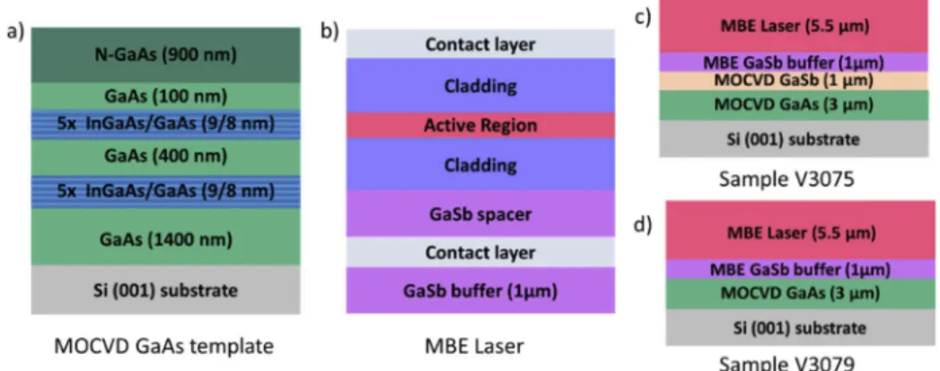
The epitaxial growth was carried out in two steps, first the MOCVD growth of the template and then the MBE growth of the laser structure. Two series of LDs were grown. Both had the same GaAs-based buffer structure grown by MOCVD that is depicted in Fig.1(a). The wafer was then taken out of the reactor and cut in several pieces. One piece was reloaded into the MOCVD reactor to grow an additional 1-µm-thick GaSb buffer layer whereas another piece was kept as-grown. Both wafers were then shipped to another laboratory for laser growth by MBE. Nominally identical GaSb-based laser structures comprising a 1-µm-thick GaSb buffer layer [Fig.1(b)] were then grown by MBE on both templates, as schematically depicted in Fig.1(c) and1(d). Detailed descriptions of the epitaxial growth steps are given below.
Fig. 1. Sketch of the layer structure of a) the MOVPE GaAs template, b) the MBE laser
structure, c) sample V3075 with GaSb buffer layer grown by MOCVD. d) sample V3079 without GaSb buffer layer grown by MOCVD.
2.1. MOCVD growth
Figure1(a) depicts the growth structure of the GaAs-on-planar Si (GoPS) template. The ∼3-µm-thick GaAs thin film was grown on a blanket 4-inch nominal (001) Si substrate with an unintentional miscut angle of less than 1°. Prior to growth, the Si substrate was subjected to a dilute HF treatment to remove the native oxide. Immediately after, the Si wafer was loaded into the AIX-200/4 MOCVD system. After annealing at 800°C for 15 min under H2ambient, the
temperature was lowered down to 400°C for the growth of a 10-nm-thick GaAs nucleation layer. Subsequently, a 1.4 µm thick GaAs layer was grown at step-increased temperatures from 550°C to 600°C. No antiphase boundaries (APBs) were observed due to their self-annihilations during the high temperature GaAs growth [28]. Five periods of thermal cycle annealing (TCA) between
750°C and 350°C were introduced within the 1.4 µm GaAs layer to propel and annihilate some of the TDs. In addition, two stacks of five-period In0.154Ga0.846As/GaAs strained layer superlattices
(SLSs) were embedded to further filter the threading dislocations. A 900 nm thick Si-doped GaAs layer was grown on top. The threading dislocation density (TDD) of the GoPS template was quantized at 1.4×108cm−2by both cross-sectional transmission electron microscopy (TEM) and electron channeling contrast imaging (ECCI) methods.
The as-grown GoPS template was cleaved for the following GaSb growth by both MOCVD and MBE systems. Regarding the GaSb growth by MOCVD, the 1-µm-thick GaSb buffer was grown at 535°C. The reactor pressure was 100 mbar and a V/III ratio as low as 1.9 was utilized to optimize the GaSb surface morphology. An interfacial misfit dislocation array was formed at the GaSb/GaAs hetero-interface [29]. To further smooth the GaSb surface as well as to reduce the dislocation density, two periods of 10 nm InAs/10 nm GaSb SLSs were inserted and grown at 500°C. As a result of the smooth GaAs growth front (roughness as low as 1.3 nm) and the optimized growth condition for the GaSb thin film, the final surface roughness of the GaSb grown on GoPS template is 1.6 nm based on a 10×10 µm2AFM measurement.
2.2. MBE growth
The samples were first cleaned with organic solvents and oxygen plasma in order to remove any possible contaminant before being loaded into the MBE reactor. Depending on the buffer layer, the samples were treated differently. Sample V3075, with a MOCVD GaSb buffer layer, was deoxidized at 550°C under an Sb flux. Sample V3079, with a GaAs buffer layer, was deoxidized at 600°C under As flux, before a thin GaAs layer was grown to smooth out the surface. Beside substrate preparation, the laser growth-sequence was the same for both samples and is nominally identical to that reported in Ref. [27]. First, a 1 µm thick n-type GaSb buffer layer was grown at 500°C. The substrate temperature was then decreased down to 450°C for the growth of a n-doped, 500-nm-thick InAsSb layer, which acts as the bottom contact of the laser structure and a marker in LD processing. Another 1 µm thick n-GaSb layer was grown to avoid any overlap of the optical mode with the InAsSb layer. The active region, designed to emit at 2.3 µm, comprised two Ga0.67In0.33As0.12Sb0.88QWs confined by Al0.25Ga0.75As0.02Sb0.98barrier layers and was
inserted at the center of a 800-nm-thick Al0.25Ga0.75As0.02Sb0.98waveguide, itself cladded by
1.3 µm thick Al0.9Ga0.1As0.07Sb0.93layers. The bottom cladding was n-doped while the top one
was p-doped. Finally, a 350 nm thick p-doped GaSb layer was grown for the top contact. All layers from the LD stack were lattice-matched to GaSb besides the QWs, which exhibited a 1.5% lattice-mismatch. X-ray diffraction confirmed full relaxation of the laser structure with respect to the Si substrate whereas the QWs were strained with respect to GaSb.
3. Laser diode fabrication process
The process was based on standard UV photolithography and inductively coupled plasma etching. The LDs ridges were 100 and 10 µm wide. The material used for electrical isolation and sidewall protection was a 350 nm thick layer of Si3N4deposited by plasma-enhanced chemical vapor
deposition. Reactive ion etching was used to open windows in the insulation layers before deposition of the electrical contacts. Both of them were taken on the top of the samples: p-contact on top of the ridges and n-contacts on the InAsSb layers. For both n- and p- contacts, Ti/Au (20/400 nm) layers were deposited by sputtering. Finally, the sample substrates were mechanically thinned down and laser bars were cleaved to different cavity lengths. No facet treatment was applied. The LDs bars were soldered epi-side-up with In on Cu heat-sinks and characterized on a probe station.
The LDs fabrication process was carried out in parallel for both samples. However, we observed the formation of cracks on sample V3075, which has a thicker buffer layer, whereas no crack was observed on sample V3079. Cracks typically arise during thermal cycles because
of the different thermal-expansion coefficients of the III-V and Si materials. The V3075 is 1-µm-thicker than the sample V3079, which results in epitaxial thickness for samples V3075 and V3079 of 10.5µm and 9.5 µm, respectively. Our observation thus gives a good estimation of the thickness limit to avoid crack formation. Still, the cracks in V3075 were running parallel to the LDs ridges. Selecting LDs where the cracks were outside the ridges allowed to reliably assess the LDs performance.
4. Laser diode properties 4.1. Threshold current densities
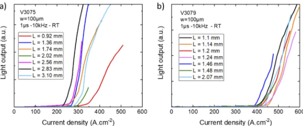
Broad area LDs with 100 µm wide ridges were measured at RT under pulsed excitation (10 kHz repetition rate and 1 µs long pulse). The light output was collected by a cooled InSb photodetector. This configuration allows to precisely know the current injection-area and the device temperature, thus giving an accurate access to the threshold current density of the laser structures.
LDs of different cavity lengths, ranging from 1 to 3 mm were tested. Each cavity length has been measured individually after cleavage for better accuracy. Light output vs current density curves are shown in Fig.2for both series of LDs.
Fig. 2. Light output vs current density curves under pulsed regime at RT. a) LDs with
MOVPE GaSb buffer layer. b) LDs without MOVPE GaSb buffer layer.
The threshold current density is in the 250–350 A.cm−2range for sample V3075 (with MOCVD
GaSb buffer), Fig.2(a), whereas it is in the 400–450 A.cm−2range for sample V3079 (without a
MOCVD GaSb buffer), Fig.2(b). These results reveal a reduction of the threshold current density as large as 40% with the thickest buffer layer. Several parameters can explain this behavior. A thicker buffer layer will result in lower defect densities and thus in better laser performance [30]. Further, the InAs/GaSb SLSs inserted within the MOCVD GaSb buffer layer acted as a defect filtering layer and promoted the formation of a smooth surface, as revealed by AFM. A reduction of the TDs density could also arise from the larger thermal budget applied to the buffer stack during the oxide removal steps. Indeed, even though the oxide removal step for the sample without MOCVD GaSb layer (V3079) was performed at high temperature (600 °C), it took place before the transition to GaSb growth which created new TDs due to the ∼8% lattice-mismatch between GaSb and GaAs. The benefit of the thermal annealing occurring during the GaAs oxide removal step could therefore be mitigated by the subsequent relaxation of the GaSb layer. In contrast, when the MBE growth started on the GaSb layer grown by MOCVD (V3075), two oxide-removal steps were carried out. First, the GaAs buffer layer was annealed at 650°C in the MOCVD reactor prior to the MOCVD growth of the GaSb buffer layer. Then, the whole MOCVD stack was annealed in the MBE reactor for GaSb oxide removal. Thus, the TDs created to relax the strain at the GaSb/GaAs interface also experienced annealing, which increased
their probability of interaction and annihilation. This is consistent with previous studies that demonstrated the effectiveness of thermal annealing to reduce the defect density in GaAs layers grown on Si [31,32] or GaSb layers grown on GaAs substrates [33]. Our work show that a detailed study including a transmission electron microscopy analysis is needed to precisely assess the impact of every growth parameter on the defect structure of such samples. It is however beyond the scope of this paper.
Previous GaSb-based LDs grown by MBE on MOCVD GaSb-on-Si templates exhibited threshold current densities in the 650–700 A.cm−2range. The GaSb MOCVD buffer layer did not include dislocation filters and was 500 nm thick, resulting in a total buffer layer thickness of 1.5 µm [27]. In contrast, all-MBE LDs grown on on-axis Si substrates exhibited threshold current densities in the 400–500 A.cm−2with a 1-µm-thick buffer layer [26]. These values are similar to
that obtained with V3079 with a 4-µm-buffer layer. Finally, it is noticeable that for sample V3075 the buffer-layer stack included SLSs, was 5 µm and experienced an additional annealing cycle, which lead to record threshold current densities. Altogether these results demonstrate that there is a large room for improvement in terms of threshold current densities of GaSb LDs grown on Si by a careful adjustment of the buffer layer thickness and/or compositions, and of the annealing sequence, and that a combined MOCVD / MBE growth scheme might be an appealing solution. 4.2. Ridge laser diodes
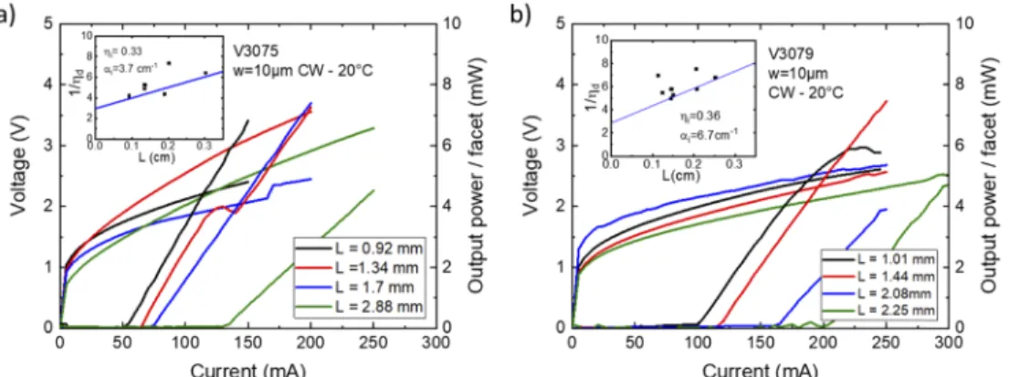
Next, narrow ridge LDs were measured at RT under CW. The light output was collected using a calibrated power-meter. Figure3shows the power-current-voltage (P-I-V) curves measured from 10 µm wide ridges and various cavity lengths for both V3075 and V3079 samples.
Fig. 3. P-I-V curves under CW regime at RT a) LDs with MOVPE GaSb buffer layer. b)
LDs without MOVPE GaSb buffer layer. The insets show the evolution of the inverse of the external quantum efficiency as function of the cavity length.
The turn-on voltage is around 1 V for both samples, close the expected value for the designed QWs structure. The serial resistance varies from 4 to 6 Ω for sample V3079, comparable to values found for for GaSb based laser [22]. In contrast, for sample V3075, the resistance is slightly higher and ranges from 5 to 11 Ω. This might be related to bubbles detected on the bottom contact for this sample, which means the adhesion between the metal and the semiconductor was not ideal. However, the threshold current is lower for this sample, 50 mA for a 0.92 mm cavity length and up to 130 mA for a 2.88 mm long one. For the LDs without the MOCVD grown GaSb buffer layer (V3079), it varies from 100 to 200 mA. The output power per uncoated facet reaches several mW for both samples.
The external quantum efficiency above threshold ηdwas extracted from the L-I curves. We
fitting the experimental data with Eq. (1) [34], 1 ηd = 1 ηi + αi ηiln(R−1) L (1)
ηibeing the internal quantum efficiency, αithe internal losses, R the reflectivity of the facets
and L the cavity length. We assumed R to be 0.3 for cleaved facets. From this analysis, we extracted the values for ηifrom the intercept of the curves. We obtained very similar values for
both samples (33 and 36%). However, αiis notably different, being 3.7 cm−1for sample V3075,
close to the typical values found for such material system, [35] and αi= 6.7 cm−1for sample
V3079. These higher performances of sample V3075 outline again the impact of the buffer layer sequence.
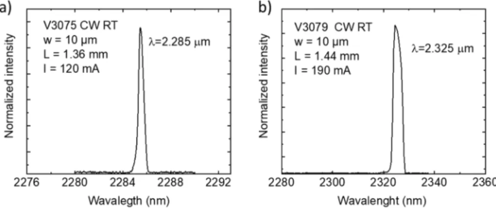
Spectra under CW regime at RT were the measured using a grating spectrometer coupled to a cooled InSb photodetector. Figure4presents the obtained spectra for 10 µm wide ridges LDs taken under an injection current 50% higher than the threshold current.
Fig. 4. Emission spectra under CW at RT a) LDs with MOVPE GaSb buffer layer. b) LDs
without MOVPE GaSb buffer layer.
The emission wavelength is around 2.3 µm for both samples, as expected from the laser design, different cavity lengths and drive currents result in slightly different wavelengths.
Finally, we have performed L-I-V measurements at various temperatures, from 20°C up to 70°C, limited by our experimental set-up. The measurement was performed in CW regime with narrow ridge diodes. In Fig.5(a) we show the results obtained for sample V3075, with a MOCVD GaSb buffer layer. The threshold current increases from 70 mA at 20°C up to 145 mA at 70°C. For sample V3079 [Fig.5(b)] it increases from 170mA at 20°C up to 220mA at 70°C. It is worth mentioning that no appreciable thermal rollover for any of the samples could be observed, and the output power per facet reaches several mW over the whole temperature range.
The usual characteristic-temperatures can be extracted from the evolution with temperature of the threshold current (T0) and external quantum efficiency (T1), which are represented in a
semi-logarithmic plot in the insets of Fig.5. The samples show different characteristic temperatures: T0= 75 K and T1= 116 K for sample V3075, T0= 102 K and T1= 134 K for sample V3079.
In contrast to the other properties, sample V3079 performs better and shows a better thermal stability. This could be due to the higher series resistance of V3075 leading to stronger Joule heating. To clarify this point, we repeated the temperature-dependent measurements in pulsed regime (not shown). As expected, the T0temperatures increased for both samples: T0= 97 K
for V3075 and T0= 114 K for V3079. It is noticeable however that the T0-difference between
CW and pulsed regime is larger for V3075 than for V3079, which confirms that at least part of the poorer thermal behavior of V3075 arose from the higher series resistance that induced Joule
Fig. 5. L-I-V curves in CW at various temperatures. a) LDs with MOVPE GaSb buffer
layer. b) LDs without MOVPE GaSb buffer layer. The insets show the evolution of the current threshold and the external quantum efficiency as function of the temperature.
heating. Other reasons could be a higher thermal resistance due to cracks in the sample and/or to the thicker buffer layer.
5. Conclusion
We have demonstrated GaSb-based LDs grown by MBE on MOCVD GaAs-on-Si template. Two series of samples were studied, for the first one, GaAs-based buffer layer was grown by MOCVD prior to the growth of the GaSb-based laser heterostructure by MBE. For the second series, a 1-µm thick GaSb buffer layer with InAs/GaSb SLSs was grown by MOCVD on top of the GaAs based buffer before the growth of the laser by MBE, which implies an additional annealing step during oxide removal. Both samples exhibited low threshold current density and CW operation at high temperature. However, the second series of LDs, with the additional GaSb buffer layer grown by MOCVD, exhibited better performance despite the appearance of cracks during processing which sets an upper thickness limit for practical applications. Narrow ridge LDs showed threshold current as low as 50 mA in CW regime with light output power of several mW and CW operation up to 70°C (set-up limited) without thermal rollover. Threshold current densities were in the range 250–350 A/cm2.
These results reveal that the performances of GaSb LDs grown on Si can largely be improved by a careful adjustment of the buffer layer thickness and/or compositions, and of the annealing sequence, and call for detailed investigations of these parameters.
Funding.Investments for the Future (ANR-11-EQPX-0016); H2020 Program of the European Union (REDFINCH, GA 780240).
Disclosures.The authors declare no conflicts of interest.
References
1. D. Thomson, A. Zilkie, J. E. Bowers, T. Komljenovic, G. T. Reed, L. Vivien, D. Marris-Morini, E. Cassan, L. Virot, J. M. Fédéli, J. M. Hartmann, J. H. Schmid, D. X. Xu, F. Boeuf, P. O’Brien, G. Z. Mashanovich, and M. Nedeljkovic, “Roadmap on silicon photonics,”J. Opt.18(7), 073003 (2016).
2. J. Wang and L. R. Chen, “Low crosstalk Bragg grating/Mach-Zehnder interferometer optical add-drop multiplexer in silicon photonics,”Opt. Express23(20), 26450 (2015).
3. H. Wu, Y. Tan, and D. Dai, “Ultra-broadband high-performance polarizing beam splitter on silicon,”Opt. Express 25(6), 6069 (2017).
4. N. Hattasan, L. Cerutti, J. B. Rodriguez, E. Tournié, D. Van Thourhout, and G. Roelkens, “Heterogeneous GaSb/SOI mid-infrared photonic integrated circuits for spectroscopic applications,”Proc. SPIE7945, 79451K (2011).
5. Y. H. Jhang, K. Tanabe, S. Iwamoto, and Y. Arakawa, “InAs/GaAs quantum dot lasers on silicon-on-insulator substrates by metal-stripe wafer bonding,”IEEE Photonics Technol. Lett.27(8), 875–878 (2015).
6. A. H. Atabaki, S. Moazeni, F. Pavanello, H. Gevorgyan, J. Notaros, L. Alloatti, M. T. Wade, C. Sun, S. A. Kruger, H. Meng, K. Al Qubaisi, I. Wang, B. Zhang, A. Khilo, C. V. Baiocco, M. A. Popović, V. M. Stojanović, and R. J. Ram, “Integrating photonics with silicon nanoelectronics for the next generation of systems on a chip,”Nature556(7701),
349–354 (2018).
7. A. Spott, E. J. Stanton, A. Torres, M. L. Davenport, C. L. Canedy, I. Vurgaftman, M. Kim, C. S. Kim, C. D. Merritt, W. W. Bewley, J. R. Meyer, and J. E. Bowers, “Interband cascade laser on silicon,”Optica5(8), 996 (2018).
8. J. E. Bowers and A. Y. Liu, “A comparison of four approaches to photonic integration,” 2017 Opt. Fiber Commun. Conf. Exhib. OFC 2017 - Proc. 2–4 (2017).
9. A. Y. Liu and J. Bowers, “Photonic integration with epitaxial III-V on silicon,”IEEE J. Sel. Top. Quantum Electron. 24(6), 1–12 (2018).
10. H. Kroemer, “Polar-on-nonpolar epitaxy,”J. Cryst. Growth81(1-4), 193–204 (1987).
11. H. Kawanami, “Heteroepitaxial technologies of III–V on Si,”Sol. Energy Mater. Sol. Cells66(1-4), 479–486 (2001).
12. D. Liang and J. E. Bowers, “Recent progress in lasers on silicon,”Nat. Photonics4(8), 511–517 (2010).
13. Q. Li and K. M. Lau, “Epitaxial growth of highly mismatched III-V materials on (001) silicon for electronics and optoelectronics,”Prog. Cryst. Growth Charact. Mater.63(4), 105–120 (2017).
14. L. Megalini, S. Šuran Brunelli, W. Charles, A. Taylor, B. Isaac, J. Bowers, and J. Klamkin, “Strain-Compensated InGaAsP Superlattices for Defect Reduction of InP Grown on Exact-Oriented (001) Patterned Si Substrates by Metal Organic Chemical Vapor Deposition,”Materials11(3), 337 (2018).
15. A. Castellano, L. Cerutti, J. B. Rodriguez, G. Narcy, A. Garreau, F. Lelarge, and E. Tournié, “Room-temperature continuous-wave operation in the telecom wavelength range of GaSb-based lasers monolithically grown on Si,”APL Photonics2(6), 061301 (2017).
16. Y. Xue, W. Luo, S. Zhu, L. Lin, B. Shi, and K. M. Lau, “155 Mm Electrically Pumped Continuous Wave Lasing of Quantum Dash Lasers Grown on Silicon,”Opt. Express28(12), 18172 (2020).
17. S. Zhu, B. Shi, Q. Li, and K. M. Lau, “1.5 µ m quantum-dot diode lasers directly grown on CMOS-standard (001) silicon,”Appl. Phys. Lett.113(22), 221103 (2018).
18. J. Kwoen, B. Jang, J. Lee, T. Kageyama, K. Watanabe, and Y. Arakawa, “All MBE grown InAs/GaAs quantum dot lasers on on-axis Si (001),”Opt. Express26(9), 11568 (2018).
19. J. Kwoen, B. Jang, K. Watanabe, and Y. Arakawa, “High-temperature continuous-wave operation of directly grown InAs/GaAs quantum dot lasers on on-axis Si (001),”Opt. Express27(3), 2681 (2019).
20. . “Global industry analysts, Inc.,” www.strategyr.com.
21. I. E. Gordon, L. S. Rothman, C. Hill, R. V. Kochanov, Y. Tan, P. F. Bernath, M. Birk, V. Boudon, A. Campargue, K. V. Chance, B. J. Drouin, J. M. Flaud, R. R. Gamache, J. T. Hodges, D. Jacquemart, V. I. Perevalov, A. Perrin, K. P. Shine, M. A. H. Smith, J. Tennyson, G. C. Toon, H. Tran, V. G. Tyuterev, A. Barbe, A. G. Császár, V. M. Devi, T. Furtenbacher, J. J. Harrison, J. M. Hartmann, A. Jolly, T. J. Johnson, T. Karman, I. Kleiner, A. A. Kyuberis, J. Loos, O. M. Lyulin, S. T. Massie, S. N. Mikhailenko, N. Moazzen-Ahmadi, H. S. P. Müller, O. V. Naumenko, A. V. Nikitin, O. L. Polyansky, M. Rey, M. Rotger, S. W. Sharpe, K. Sung, E. Starikova, S. A. Tashkun, J. Vander Auwera, G. Wagner, J. Wilzewski, P. Wcisło, S. Yu, and E. J. Zak, “The HITRAN2016 molecular spectroscopic database,”J. Quant. Spectrosc. Radiat. Transfer203, 3–69 (2017).
22. A. Baranov and E. Tournié, Semiconductor Lasers: Fundamentals and Applications (2013). 23. E. Tournié and L. Cerutti, Mid-Infrared Optoelectronics, 1st ed. (Elsevier, 2020).
24. J. R. Reboul, L. Cerutti, J. B. Rodriguez, P. Grech, and E. Tournié, “Continuous-wave operation above room temperature of GaSb-based laser diodes grown on Si,”Appl. Phys. Lett.99(12), 121113 (2011).
25. H. Nguyen-Van, A. N. Baranov, Z. Loghmari, L. Cerutti, J.-B. Rodriguez, J. Tournet, G. Narcy, G. Boissier, G. Patriarche, M. Bahriz, E. Tournié, and R. Teissier, “Quantum cascade lasers grown on silicon,”Sci. Rep.8(1), 7206
(2018).
26. M. Rio Calvo, L. Monge Bartolomé, M. Bahriz, G. Boissier, L. Cerutti, J.-B. Rodriguez, and E. Tournié, “Mid-infrared laser diodes epitaxially grown on on-axis (001) silicon,”Optica7(4), 263 (2020).
27. L. Monge Bartolomé, T. Cerba, D. Diaz-Thomas, M. Bahriz, M. Rio Calvo, G. Boissier, T. Baron, J.-B. Rodriguez, L. Cerutti, and E. Tournie, “Etched-cavity GaSb laser diodes on a MOVPE template grown on a 300-mm Silicon wafer,”
Opt. Express28(14), 20785–20793 (2020).
28. Y. Wan, C. Shang, J. Norman, B. Shi, Q. Li, N. Collins, M. Dumont, K. M. Lau, A. C. Gossard, and J. E. Bowers, “Low Threshold Quantum Dot Lasers Directly Grown on Unpatterned Quasi-Nominal (001) Si,”IEEE J. Sel. Top. Quantum Electron.26(2), 1–9 (2020).
29. Q. Li, B. Lai, and K. M. Lau, “Epitaxial growth of GaSb on V-grooved Si (001) substrates with an ultrathin GaAs stress relaxing layer,”Appl. Phys. Lett.111(17), 172103 (2017).
30. C. Hantschmann, Z. Liu, M. Tang, S. Chen, A. J. Seeds, H. Liu, I. H. White, and R. V. Penty, “Theoretical Study on the Effects of Dislocations in Monolithic III-V Lasers on Silicon,”J. Lightwave Technol.38(17), 4801–4807 (2020).
31. J. W. Lee, H. Shichijo, H. L. Tsai, and R. J. Matyi, “Defect reduction by thermal annealing of GaAs layers grown by molecular beam epitaxy on Si substrates,”Appl. Phys. Lett.50(1), 31–33 (1987).
32. D. Jung, P. G. Callahan, B. Shin, K. Mukherjee, A. C. Gossard, and J. E. Bowers, “Low threading dislocation density GaAs growth on on-axis GaP/Si (001),”J. Appl. Phys.122(22), 225703 (2017).
33. R. T. Hao, J. Guo, S. K. Deng, Y. Liu, Y. M. Miao, and Y. Q. Xu, “Rapid Thermal Annealing on GaSb Thin Films Grown by Molecular Beam Epitaxy on GaAs Substrates,”Adv. Mater. Res.787, 143–147 (2013).
34. L. A. Coldren, S. W. Corzine, and M. L. Mašanović, Diode Lasers and Photonic Integrated Circuits, second (John Wiley & Sons, Inc., 2012).
35. A. Salhi, Y. Rouillard, J. Angellier, and M. Garcia, “Very-low-threshold 2.4-µm GaInAsSb-AlGaAsSb laser diodes operating at room temperature in the continuous-wave regime,”IEEE Photonics Technol. Lett.16(11), 2424–2426