A DC Stabilized Fully Differential Amplifier
by
Nancy Y. Sun
Submitted to the Department of Electrical Engineering and Computer
Science
in partial fulfillment of the requirements for the degree of
Masters of Engineering in Electrical Engineering
at the
MASSACHUSETTS INSTITUTE OF TECHNOLOGY
September 2005
@
Nancy Y. Sun, MMV. All rights reserved.
The author hereby grants to MIT permission to reproduce and
distribute publicly paper and electronic copies of this thesis document
in whole or in part.
A uthor . ...
Department of Electrical Engineering and Computer Science
June 27, 2005
Certified by
....
SOhida Martinez
Senior Engineer, Charles Stark Draper Laboratory
Thesis Supervisor
C ertified by.
...
Eric Hildebrant
Principal Engineer, Charles Stark Draper Laboratory
Thesis Supervisor
Certified by...:
. . ...
Joel L. Dawson
Assistant Professor of EIetr4ca}Egineerig and Computer Science
-upervisor
Accepted by.
Arthur C. Smith
Chairman, Department Committee on Graduate Students
MASSACHUSETTS NSTmrTE OF TECHNOLOGY
M
TL
b res
Document Services Room 14-0551 77 Massachusetts Avenue Cambridge, MA 02139 Ph: 617.253.2800 Email: [email protected] http://libraries.mit.edu/docsDISCLAIMER OF QUALITY
Due to the condition of the original material, there are unavoidable flaws in this reproduction. We have made every effort possible to
provide you with the best copy available. If you are dissatisfied with this product and find it unusable, please contact Document Services as soon as possible.
Thank you.
The images contained in this document are of
the best quality available.
A DC Stabilized Fully Differential Amplifier
by
Nancy Y. Sun
Submitted to the Department of Electrical Engineering and Computer Science on June 27, 2005, in partial fulfillment of the
requirements for the degree of
Masters of Engineering in Electrical Engineering
Abstract
The conventional method of constructing a gain amplifier is to use resistor feedback networks. However, present CMOS technology provides capacitors that offer sub-stantially better tracking and linearity performance over variations in temperature. Draper Laboratory's High Performance Gyroscope currently employs two single-ended amplifiers configured to work fully differentially. Gain is provided with capacitive feedback, but DC stabilization of the amplifiers, necessary to provide bias to the am-plifier and prevent output saturation, is achieved with large, external resistors. In this thesis, a fully-differential gain amplifier using capacitive feedback is proposed. An integratable, on-chip DC stabilization network is also presented.
Thesis Supervisor: Ochida Martinez
Title: Senior Engineer, Charles Stark Draper Laboratory Thesis Supervisor: Eric Hildebrant
Title: Principal Engineer, Charles Stark Draper Laboratory Thesis Supervisor: Joel L. Dawson
Acknowledgments
The work presented in this thesis was made possible by many people at the Charles Stark Draper Laboratory. More specifically, I would like to thank my Draper advisors Ochida Martinez and Eric Hildebrant. Ochida's knowledge, experience, and insight were invaluable parts of my experience at Draper. Through her mentorship, she taught me not just about circuits, but also about patience and completeness. Eric's wittiness always kept me on my toes and his wisdom provided guidance throughout this project. I would also like to thank some others who made my time at Draper more enjoyable: John Lachapelle for his kindness and intuition, Sam Beilin for his stories, and John Puskarich for his collaboration.
I would also like to thank my MIT thesis advisor Professor Joel Dawson for his ideas and advice.
There are many others who have made my time at MIT all the more enjoyable. To my teammates and coaches, past and present, of the MIT women's ultimate team,
I owe thanks for the distractions, lessons, and countless memories. I am lucky to have
shared the field with you. To the usual suspects: Pam Chang, Howard Chou, Harold
Hsiung, LeeAnn Kim, Matt Park, Carlos Renjifo, Jenny Ta, and Suzanne Young
-thanks for keeping me sane.
My love and appreciation also go out to my Mom and Dad, for their care and
support, as well as my brothers Jeff and Andrew, Grandma Lily, and Aunt Joan. This thesis was prepared at The Charles Stark Draper Laboratory, Inc., under Contract B54530612, sponsored by Honeywell International Inc., Minneapolis, Min-nesota.
Publication of this thesis does not constitute approval by Draper or the sponsoring agency of the findings or conclusions contained herein. It is published for the exchange and stimulation of ideas.
Permission is hereby granted to the Massachusetts Institute of Technology to reproduce any or all of this thesis.
Nancy Y. Sun
Contents
1 Overview
1.1 Gyroscope System Overview
1.1.1 Sense Channel . . . .
1.1.2 Motor Position Channel .
1.2 Thesis Scope . . . . 1.2.1 Temperature Sensitivity of gies . . . . 1.2.2 Motivation . . . . 1.2.3 Performance Requirements 1.2.4 Thesis Outline . . . . . . . . . . . . . . . . . . . .
Gain Amplifier Closed-Loop
Topolo-. Topolo-. Topolo-. Topolo-. Topolo-. Topolo-. Topolo-. Topolo-. Topolo-. Topolo-. Topolo-. Topolo-. Topolo-. Topolo-. Topolo-. Topolo-. Topolo-. Topolo-. Topolo-. Topolo-. . . . . . . . . . . . . 2 Op-Amp Topology 2.1 Folded-Cascode Architecture . . . .
2.1.1 DC Small Signal Gain . . . .
2.1.2 Frequency Response . . . .
2.1.3 Alternative calculations . . . .
2.1.4 Noise [9, 4, 6] . . . .
2.1.5 Noise in the Folded-Cascode Op-Amp . . . .
2.2 Common Mode Feedback . . . .
2.2.1 Why is Common Mode Feedback Necessary?
2.2.2 Continuous-Time common mode Feedback
2.3 Gain-Enhancement through Active Cascoding . . .
2.3.1 Regular Cascode . . . . 17 18 18 18 20 20 22 22 25 27 27 28 29 30 32 35. 37 37 39 44 44
2.3.2 Basic Active Cascode Architecture . . . .
2.3.3 Implementation of the Active Cascode Technique
2.4 Folded-Cascode Op-Amp Simulation Results . . . .
2.4.1 AC Simulations . . . .. . . .
2.4.2 Output Swing . . . .
2.4.3 CM FB Loop . . . .
3 Capacitive Feedback
3.1 The Basic Capacitive Feedback Gain Topology
3.2 Adding a Feedback Resistor . . . .
3.3 Using an OTA as a DC Stabilizer . . . .
4 DC Stabilization Network
4.1 Review of Second Order Systems [3, Sec 2.6] . . . .
4.2 DC Stabilizer Loop Analysis . . . .
4.2.1 Closed-Loop Transfer Function and AC Response
4.3 Component Description . . . .
4.3.1 Back-to-Back Diodes . . . .
4.3.2 Noise Shunting Capacitor . . . .
4.3.3 Operational Transconductance Amplifier (OTA)
4.3.4 Diode Capacitance .. . . . .
4.4 Sum m ary . . . .
5 Gain Amplifier System Simulation Results 5.1 AC Simulations . . . . 5.1.1 Gain and Magnitude . . . . 5.1.2 N oise . . . .
5.1.3 Phase Shift and Gain Stability . . .
5.1.4 Static Phase Shift . . . .
5.1.5 Loop Gain . . . . 5.2 Transient Simulations . . . . 46 49 51 54 58 59 61 61 62 63 65 66 68 68 70 70 73 74 78 79 83 83 83 86 87 88 89 90 . . . . . . . . . . . .
5.2.1 Total Harmonic Distortion . . . . 90
6 Conclusion 93 6.1 Future Recommendations . . . . 93
A Circuit Configurations 95 A.1 Final schematics . . . . 95
A.1.1 Summary of Device Sizes . . . . 100
A.2 Circuit Configurations for Simulations . . . . 103
A.2.1 Folded Cascode Op-Amp . . . . 103
A.2.2 Gain Amplifier System . . . 108
A.2.3 AC Response . . . . 110
----List of Figures
Gyroscope Block diagram. . . . .
Gain amplifier with resistive feedback. . . . .
Block diagram of a typical op-amp. . . . .
Block diagram of an inverting amplifier. . . . .
Magnitude plot of various closed-loop gains. . . . . 2-1 A fully-differential folded-cascode op-amp . . . . 2-2 A two-port model of the fully-differential folded-cascode. . . .
2-3 The op-amp half circuit and its small signal model equivalent.
2-4 Circuit Models for Thermal Noise . . . . Small signal noise model for a MOSFET. . . . .
Noise spectral density for a MOSFET. . . . . half circuit model of the CMFB circuit. . . . . Block diagram of a typical CMFB network ([4], 818). CMFB using a resistive divider and amplifier... CMFB schematic. . . . . Folded-cascode schematic. . . . . Cascode topology. . . . . Source degeneration... Active cascode and its equivalent small signal model. Single transistor active cascoding. . . . .
. . . . 19 . . . . 20 . . . . 24 . . . . 25 . . . . 26 . . 28 . . 29 . . 31 . . 33 . . 34 . . 35 . . 37 . . 38 . . 40 . . 41 . . 42 . . 45 . . 46 . . 47 . . 48
2-16 Four single-ended amplifiers used for Active cascoding in a fully-differential
folded-cascode. . . . . 50 1-1 1-2 1-3 1-4 1-5 2-5 2-6 2-7 2-8 2-9 2-10 2-11 2-12 2-13 2-14 2-15
2-17 Two differential amplifiers used for active cascoding in a
fully-differential folded-cascode. . . . . 51
2-18 Fully Differential Gain Enhancement Amplifiers. . . . . 52 2-19 Bode plot of the op-amp in an open-loop configuration. The unity gain
frequency is labeled on the plot. . . . . 54
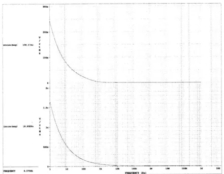
2-20 Output and input referred noise of the op-amp. The noise at 8kHz is
labeled on the plot. . . . . 55
2-21 The upper plot shows the common mode gain of the op-amp. The
lower plot shows the common mode rejection ratio. . . . . 56
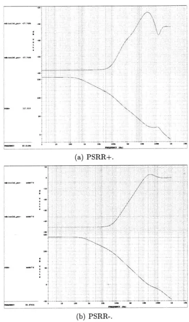
2-22 Upper plots show the power supply gain. Lower plots show the power
supply rejection ratio. . . . . 57
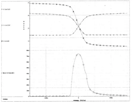
2-23 Output swing of the op-amp. The upper plot shows the output voltage
as the input voltage is swept, and the lower plot shows the derivative
of one of the outputs. . . . . 58
2-24 Bode plot of the open-loop configuration of the op-amp CMFB network 59
3-1 Capacitors as elements in a feedback path to provide gain. . . . . 61
3-2 Using a feedback resistor to provide DC stabilization of the op-amp. . 62
3-3 Using an OTA for DC stabilization. . . . . 64
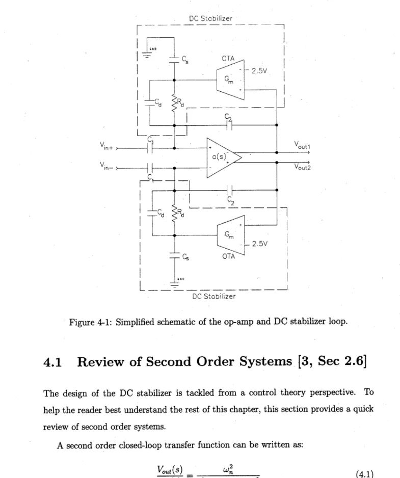
4-1 Simplified schematic of the op-amp and DC stabilizer loop. . . . . 66
4-2 Complex conjugate poles in the s-plane. System is underdamped. [3,
p .43]. . . . . 68
4-3 Op-amp block diagram . . . . 69
4-4 Back-to-back diodes . . . . 71
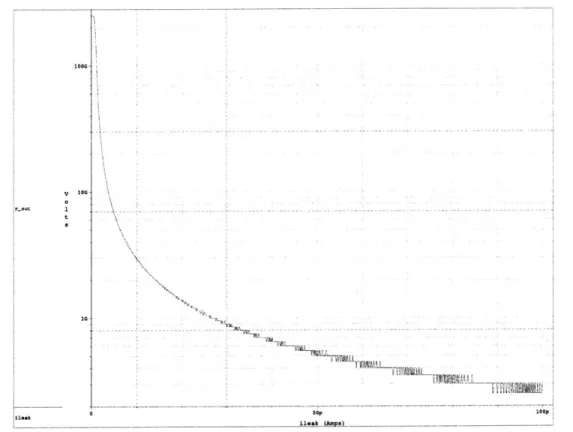
4-5 Impedance of the back-to-back diodes as a function of leakage current. 71
4-6 Bode plot of the system closed-loop response with varying C,. .. .. 74
4-7 DC sweep showing the linear range and transconductance of the OTA100MB. 76
4-8 Monte carlo simulation with a temperature sweep showing OTA offset. 77
4-9 Root locus plots of the system closed-loop response with varying
4-10 Bode plot of the system closed-loop response with varying leakage
cur-rent. Plot created with Cd = OpF. . . . . 80
4-11 Pole-zero plots of the system closed-loop response with varying leakage current. Plots created with Cd = 0.5pF. . . . . 81
4-12 Bode plot of the system closed-loop response with varying leakage cur-rent. Plot created with Cd = 0.5pF. . . . . 82
5-1 Bode plot of the closed-loop system with Cd included. . . . . 84
5-2 Bode plot of the closed-loop system with Cd removed. Notice the increased peaking . . . . 85
5-3 Output and input referred noise of the system. . . . . 86
5-4 Upper plot demonstrates gain stability, and the lower plot shows the dynamic phase shift of the system. . . . . 87
5-5 Static phase shift. . . . . 88
5-6 Loop gain. . . . . 89
5-7 Results of a transient simulation. . . . . 91
A-i Schematic for the biasing circuit. . . . . 95
A-2 Schematic for the fully-differential folded cascode op-amp. . . . . 96
A-3 Schematic for the PMOS input stage gain enhancement op-amp. . . . 97
A-4 Schematic for the NMOS input stage gain enhancement op-amp. . . . 98
A-5 Schematic for the DC stabilizer block . . . . 99
A-6 Schematic file used to perform an open-loop AC simulation on the op-am p. . . . . 103
A-7 Schematic file used to simulate the op-amp's common-mode rejection ratio. . . . . 104
A-8 Schematic used to simulate the op-amp's power-supply rejection ratio. 105 A-9 Schematic file used to simulate the op-amp's output swing. . . . . 106
A-10 Schematic file used to simulate the op-amp's CMFB loop . . . . 107
-11 Schematic file used to capture the operating points of the system at startup. . . . . 108
A-12 Schematic file used to simulate the system's Total Harmonic Distortion
(T H D ) . . . . 109
A-13 Schematic file used to simulate the system's AC response. . . . . 110
List of Tables
1.1 Performance of typical resistors in today's semiconductor processes. 21
1.2 Performance of typical capacitors in today's semiconductor processes. 21
1.3 Performance requirements of the gain amplifier system . . . . 26
2.1 Op-amp simulation results. Results are given fully differentially except for those marked with an asterisk (*), which are given as a single-ended readout. ... ... 53
4.1 Typical values of components in Figure 4-1. . . . . 67
4.2 Impedances of the back-to-back diodes for various values of leakage current. . . . . 72
5.1 System simulation results. . . . . 83
5.2 THD for various amounts of leakage current. . . . . 91
A.1 Devices sizes for the biasing networks . . . . 100
A.2 Devices sizes for the folded cascode op-amp . . . . 101
A.3 Devices sizes for the CMFB circuit . . . . 101
A.4 Devices sizes for the NMOS input gain enhancement op-amp . . . . . 101
Chapter 1
Overview
Micromechanical tuning fork gyroscopes are attractive as inertial devices because they offer system miniaturization and can be produced at low cost [2]. Advances in micro-fabrication of both sensor and accompanying electronics have led to low cost solutions for both military and commercial applications. However, in order to compete with conventional inertial systems, MEMS-scale systems must also offer high resolution and performance stability over environment variations.
Because of the miniaturization trends of inertial Micro-Electro-Mechanical Sys-tems (MEMS), reduced signal levels present great challenges for the readout elec-tronics. In digital circuits, CMOS technology has allowed for tremendous gains in chip density, power, and cost, without sacrificing performance. However, the same cannot be said for analog circuitry. One reason for this is the poor quality of the passive components available in most CMOS processes. These components, particu-larly resistors, tend to have poor tolerances and poor stability over temperature and
operating voltages.
Resistor ratios are used extensively in analog circuit design. However most CMOS processes do not offer the resistor matching required to maintain precise ratios. For-tunately, CMOS technology provides capacitors with more attractive performance characteristics. This thesis explores the substitution of capacitors for resistors in an AC gain amplifier for a Draper Laboratory MEMS gyroscope.
1.1
Gyroscope System Overview
Draper's tuning fork gyroscope takes advantage of the Coriolis Effect to sense rate of rotation. Its construction is shown in Figure 1-1. The proof masses are supported by flexure beams that allow motion in the x- and y-directions at a resonant frequency ranging from 8kHz to 25kHz. The masses are suspended above stationary sense electrodes. Application from a motor of an oscillatory electrostatic force between the combs of the proof masses and those of the left and right motor electrodes cause the proof masses to vibrate in opposite directions along the x-axis (which is often referred to as in-plane motion). The Coriolis acceleration, then, is the cross product between a mass's velocity in the x-direction and the input rate of rotation about the z-axis.
1.1.1
Sense Channel
In the presence of rotation about the z-axis, the Coriolis Effect causes the proof masses to deflect in the y-direction. This deflection or displacement is referred to as an out-of-plane motion and occurs at the same frequency as the in-plane oscillatory motion. The change in the gap between the proof masses and the sense electrodes beneath them causes a change in capacitance that is directly proportional to the magnitude of the rate of rotation. The change in capacitance induces a current that is output along the sense channel. This current is integrated by the charge amplifier circuit to produce a voltage proportional to the rate of rotation.
1.1.2
Motor Position Channel
The positions of the proof masses are sensed by the left and right center electrodes in a manner similar to how the sense electrodes beneath the proof masses sense rotation. In this case, the charge amplifier integrates a charge induced by the change in capacitance of the capacitors formed between the tines on the left and right center electrodes and the inner tines on the proof masses. The charge amplifier produces a voltage proportional to the position of the proof masses.
Stationary Sense Pjlte
- Proof Mass A-'
Motor Position Channel
Motor Position Channel
U
C-) U
C-)
Stationary Sense_ Plate
Proof Moss B L --- - - -- - L-Ii) 0 a DC Stabilize DC Stabilizer Charge Amplifier DC Stabilizer DC Stabilize C 2 C_ SDM CC -DC Stabilize DC Stabilize
Charge Amplifier Gain Amplifier
Figure 1-1: Gyroscope Block diagram. Z x ~0 L, 0 Sense Channel
since this signal is always available once the gyroscope's motor is started. The clock generated from the position signal will be used to demodulate the input rate infor-mation to baseband. For this reason, both the motor position and the sense channels must be designed to achieve a high level of phase matching.
1.2
Thesis Scope
There are electronics needed to operate the gyroscope that are not shown in Figure
1-1, but this thesis will only focus on a portion of the readout electronics in the sense
channel. The focus of the thesis is on designing the fully differential AC gain amplifier block in Figure 1-1. The fact that the signal of interest is modulated to a frequency ranging from 8kHz to 25kHz allows us to consider substituting the typical resistive feedback network with other types of feedback networks. The following sections will discuss some of the design motivations, considerations, and requirements of the gain amplifier.
1.2.1
Temperature Sensitivity of Gain Amplifier Closed-Loop
Topologies
+ -A-+ +
Vid O(S) Vod
Figure 1-2: Gain amplifier with resistive feedback.
applica-tions so it must be able to operate with high precision in a wide range of temperatures. However, recent studies at Draper have shown that a gain amplifier using resistive feedback, like that shown in Figure 1-2, has an unacceptable drift in gain over tem-perature. Draper has shown that the on-chip resistor ratios (which are conventionally used to set gains) offer inadequate tracking over temperature, making it difficult to achieve precision gain. This issue is primarily due to the poor matching tolerance of the chosen polysilicon resistors. Furthermore, their high voltage coefficients lead to harmonic distortion. However, on-chip capacitors offer superior temperature and voltage coefficients, making them attractive feedback elements.
Tables 1.1 and 1.2 lists typical values for the most common integrated circuit resis-tors and capaciresis-tors. Temperature and voltage coefficients (TC and VC, respectively) are usually expressed in parts per million per degree Celcius (P). For example, a temperature coefficient of resistance of 100021 means that a 100Q resistance will not change more than 0.01 Q per degree Celcius change in temperature.
Unfortunately, typical CMOS processes do not offer thin-film resistors. Diffusion and N-well resistors have voltage coefficients that are too high to meet our linearity specifications. Polysilicon is a good compromise, but even with careful layout, good resistor matching is difficult to achieve.
Resistor material TC (") VC (Pv) Expected matching
Thin-film <50 <30 0.5-2%
Polysilicon 50-2000 30-150 0.5-2%
N-Well 1000-50000 50000 1-2%
Diffusion 1000 1000-10000 1-2%
Table 1.1: Performance of typical resistors in today's semiconductor processes.
Capacitor material TC (Pfl) VC (PTm) Expected matching
Poly-diffusion - -
-Metal-poly - -
-Poly-poly [7] 20-30 10-200 0.2-0.5%
1.2.2
Motivation
Because gain amplifier performance is determined by the amplifiers feedback net-work(s), the temperature coefficients and voltage coefficients of the components that comprise the feedback network are important metrics of amplifier performance. Ta-bles 1.1 and 1.2 indicate that capacitor temperature and voltage coefficients are signif-icantly better than those of resistors. This allows capacitors to track each other more accurately over temperature and voltage changes, thus minimizing harmonic distor-tion. Therefore, when component value and ratio matching is of great importance, capacitors are a more attractive option than resistors. Motivated by the insufficien-cies of on-chip resistors, this thesis will investigate the implementation of an amplifier using capacitive feedback.
1.2.3
Performance Requirements
Some of the more notable performance requirements of the gain amplifier are described in this section.
Fully Differential Topology
Fully differential circuits are desirable in analog circuit design primarily because they are useful in rejecting common-mode noise, particularly in mixed-mode design. Since a fully differential circuit is built symmetrically, noise should affect both signal paths equally. In a fully differential amplifier, the signals at the two output terminals are subtracted from each other, so any common-mode disturbances, such as power supply noise, are rejected.
Phase Shift
Phase shift is a Draper Laboratory system requirement of all components in the gyroscope system. Once the gyroscope motor is started, the motor position signal is used as a reference signal for demodulating the rate input information to baseband. In order to minimize demodulation errors (which would result in offset and gain errors),
the sense and motor position channels must posses similar phase shift characteristics. As much as possible, identical designs are used in both channels to achieve phase shift matching.
There are two primary types of phase shift:
* Static phase shift - Static phase shift is how much the closed-loop output phase varies across the desired signal frequency range. The requirement is that
static phase shift must be < 1* from 8kHz to 25kHz.
" Dynamic phase shift -Dynamic phase shift is how much the closed-loop out-put phase across the desired signal frequency range varies across temperature.
The dynamic phase must vary by < 0.50 for signals from 8kHz to 25kHz within
a temperature range of -55'C to 105*C. Errors due to dynamic phase shift are more problematic because dynamic phase shifts of the two channels are less likely to match.
Unity-Gain Frequency
The desired unity-gain frequency can be derived from the static phase shift
require-ment. The phase of a system with a single pole roll-off is given by - arctan system-3dBbandwidth,ignalfreuency
For a unity-gain configuration, this means that in order for the system to have less
than 10 of static phase shift at a signal frequency of 25kHz (the maximum resonant
frequency of the proof masses), the -3dB bandwidth of the unity-gain system (which
is also the crossover frequency of an open-loop system with 900 of phase margin) needs
to be greater than 1.5MHz. As the closed-loop gain increases, however, the system open-loop crossover frequency also needs to increase to maintain the phase shift.
To see how much the open-loop crossover frequency needs to increase, refer to the block diagram of a typical op-amp shown in Figure 1-3. We model the op-amp as a
system with a single pole roll-off having a transfer function of a(s) = , where ao
P1
is the open-loop DC gain, and pi is the single pole location. f is the feedback factor of the closed-loop configuration. For the closed-loop configuration in Figure 1-4,
+ C(S) >I Vout
Figure 1-3: Block diagram of a typical op-amp.
The gyroscope system requires that the op-amp be configured for differential
closed-loop gains from 2 to 20. With a closed-loop gain of 20 (R2 = 20k and R1 = 1k,
equivalently a feedback factor of 1), the crossover frequency of the open-loop gain needs to be increased by a factor of 21 (one over the feedback factor) in order to have less then 1' of static phase shift at a signal frequency of 25kHz. Therefore, the crossover-frequency of the op-amp must be increased from the previous figure of 1.5MHz to 31.5MHz. This is illustrated in Figure 1-5. To maintain good stability of the gain amplifier, we require that the loop gain phase margin (phase at the open-loop unity-gain frequency) be greater than 45*f.
Output Swing and Load Capacitance
The output of the gain amplifier is AC coupled to drive a E - A converter, which
digitizes all the sense channel signals. The input range of the E - A converter (5Vpp
differential) sets the output swing requirement of the gain amplifier. Similarly, the
input capacitance of the E-A converter (:; 10pF) sets the maximum load capacitance
that the gain amplifier must drive.
Noise
The total input referred noise of the gain amplifier must be < 35nV/if Hz) at 8kHz so that the noise of the amplifier does not limit the minimum resolution of the gyroscope input signal.
R2
yin - t
> out
G N 0
(a) Single ended op-amp with resistive feedback.
V-R
V ~Ri + R2(sot
R,
Ri + R2
(b) Block diagram of the single ended op-amp with resistive feed-back.
Figure 1-4: Block diagram of an inverting amplifier.
Performance Requirements Summary
Table 1.3 lists the performance requirements of the gain amplifier system.
1.2.4 Thesis Outline
The remainder of the thesis is organized as follows:
Chapter 2 describes the design of the op-amp and the motivations for the design decisions made. Chapter 3 describes the capacitive feedback network and explains why a DC stabilization network is necessary. Chapter 4 describes the design of the
DC stabilization network. Chapter 5 gives the simulation results of the gain amplifier
system. Chapter 6 summarizes the thesis and discusses possible future improvements. The appendix shows final circuit schematics and the configurations used to run sim-ulations.
gain a0O -20 1 -a(s) gain of 20 unity gain p1
(1+,)
1
21 frequency p (1+ aO )Figure 1-5: Magnitude plot of various closed-loop gains.
Power supply 5V
Load 10pF
Signal static phase shift < 1*
Signal dynamic phase shift < 0.50
Total Harmonic Distortion (THD) 60dB for 4Vpp differential output swing at
25kHz
Input Referred Noise < 35nV/ (Hz) at 8kHz
PSRR > 60dB at 25kHz
CMRR > 60dB at 25kHz
Loop gain phase margin 450
Chapter 2
Op-Amp Topology
A single stage fully differential folded-cascode op-amp is proposed in this chapter to
be used in place of the two single-ended gain amplifiers seen in Figure 1-1. Refer to Section 1.2.3 for why a fully differential topology was chosen. Since the op-amp only has to drive a capacitive load, a single stage design is proposed primarily for simplicity and ease of compensation. The main limitation of the single stage design is its small output swing. However, the output swing requirement (refer to Section 1.2.3) is within the capability of some single stage topologies.
A folded-cascode is chosen over its telescopic counterpart primarily because the
folded-cascode has increased output swing. It can swing within two VDS,SAT of both
rails, while the telescopic can swing within two VDS,SAT of one rail, but only three
VDS,SAT of the other rail. An added advantage of the folded-cascode is increased
common mode input range. By folding the input differential pair, this architecture has decoupled input swing from output swing.
2.1
Folded-Cascode Architecture
The basic fully differential folded-cascode op-amp is shown in Figure 2-1. Transistors
M, and M2 form the input differential pair. M1 2 forms a tail current source to set
the current through the differential pair. M5 and M6 form a common-gate stage to
M1 2
V
V. Vin+ F V In-V C C 7 4 M a M7 V B3 M E M 4 out- VOUt+ C CL Vi ID CM4Figure 2-1: A fully-differential folded-cascode op-amp
and M4 are the current source loads; the drain currents of these transistors are split
between the input differential pair and cascode stages.
2.1.1
DC Small Signal Gain
A two-port model of the amplifier is shown in Figure 2-2. The DC gain of this system
is aud = GMR0.
GM is the short-circuit transconductance, given by i, where ic is the output
current when the output is shorted to ground. With the output shorted to ground,
there is no current gain across M5, and isc = gmlVid, so Gm = gmi.
RO is the output impedance of the folded-cascode op-amp and is a parallel
combi-nation of the impedances looking into the drains of M5 and M7 (where /. = gm.ro,
V0C < N Gm Vi0 R, CL Vout
Figure 2-2: A two-port model of the fully-differential folded-cascode.
Ro = Ro,//Ro,dow = (#7ro9)//(#3(roj//ro3)) (2.1)
Therefore, the DC small signal gain of the system is:
avd =G MRo = gm, ((1 7r 9)//(/35(ro//ro3))) (2.2)
2.1.2
Frequency Response
Nodes of high resistance connected to a capacitive or inductive load have the most significant impact on a system's frequency response. In the circuit of Figure 2-1, the node with the largest impedance appears at the output and gives the dominant pole
P, of the system. At the output, we have the parallel combination of the output
resistance R,, and the load capacitance CL seen in Figure 2-2.
avd = mjR (2.3)
sROCL + 1
-, (2.4)
RoCL s((#7ro9)//( 35(roj//ro3)))CL
The lowest frequency non-dominant pole is due to parasitic capacitances (the sum
of the parasitics will be given by C,) at the sources of M5 and M6 [81. Cp is large
(typically on the order of .lpF) because of the following reasons [8]:
" M1 and M2 are sized to have a large ! ratio for high gm and low noise. " M3 and M4 are sized to have a large T ratio for a low VDS,SAT drop.
These parasitics create a non-dominant pole located at:
P2 = -(2.5)3
P2=-where gm3 is the transconductance of M3.
Assuming that the two poles are real and widely separated (which is a valid
assumption because CL > O, and R, >> then at the unity gain frequency, the
gain of the op-amp can be approximated by a single pole roll-off:
avd = gmiRout 9m1 (2.6)
sROutCL + I sOL
This results in a unity gain frequency at wt g.
2.1.3
Alternative calculations
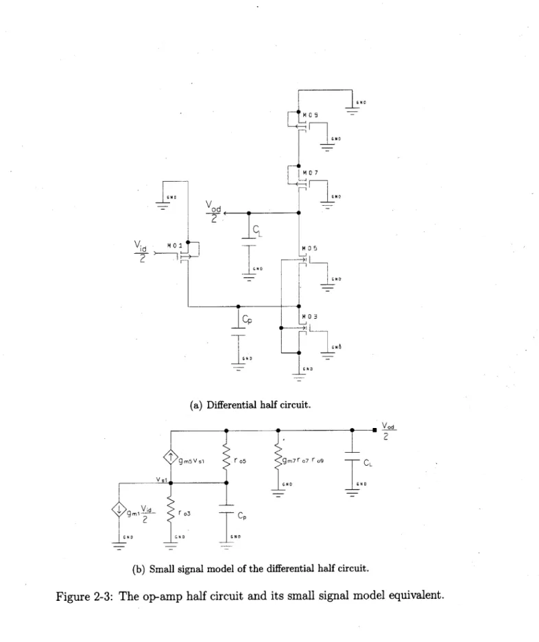
The results of Section 2.1.2 can also be derived algebraically, without the aid of conceptual insight by analyzing the differential half circuit in Figure 2-3(a) and the
corresponding small signal model in Figure 2-3(b). If we assume that gmro >> 1 and
that the output impedance looking up into the drain of M7 is very large, then:
-gmiro3/35
avd =9~O3 ( 2.7)
1 + sro3/35CL + s2ro3ro5CpCL
For this two pole transfer function, if we assume that the poles are real and widely separated, the polynomial can be approximated as:
s s+ 1 2 8 S2
P(s) = (1 - )(1 - 1 - s(- + - - + (2.8)
Pi P2 P1 P2 P1P2 P1 P1P2
By matching coefficients, pi = - RL 1 and P2 =-3, which are the same results ep
v d M IIN D 0 7 Vod CL M0 5 GN D L1 Cp GND (a) M0 3 GND
Differential half circuit.
'9gm5V sl r 05 gm7 r0o7 rog CL
V s1
gm' 1 r .3 Cp
GND G ND
(b) Small signal model of the differential half circuit.
2.1.4
Noise [9, 4, 6]
Because the gain amplifier is near the front end of the readout electronics, we must deal with noise fundamental to the circuit that is due to the discrete nature of charged particles. This noise level can be reduced through proper circuit design. There are three primary types of noise: (1) shot, (2) thermal, and (3) flicker. Since noise is random by nature, it is often expressed in root mean squared (RMS) values to indicate normalized noise power. We will begin by reviewing the three primary types of noise, and see how they are manifested in the folded-cascode op-amp.
Shot Noise
Shot noise is present wherever there is direct current flow. Current, which appears to be continuous and constant, is in reality composed of many discrete and random events. Shot noise is caused by these events. An example of shot noise is a carrier jumping the potential barrier between the p-type and n-type regions of a p-n junction.
If the current is composed of a series of discrete and random events, we denote the
average DC current by ID, the bandwidth of the circuit by Af, and the RMS current noise as [4]:
i2=2qIDAf (2.9)
From this equation, we can see that the spectral density of shot noise, 7, is
constant. Noise with a spectral density independent of frequency is also known as white noise.
Thermal Noise
Thermal noise is due to the random thermal motion of electrons in any conductor. Since electron thermal velocities are higher than electron drift velocities (the mecha-nism by which current is produced), thermal noise is independent of current. As its name indicates, thermal noise is proportional to temperature T (*K).
R
+ V 2
(a) Voltage source equivalent of thermal noise. 2 (b) Current source thermal noise. R equivalent of
Figure 2-4: Circuit Models for Thermal Noise
The voltage source and current source equivalent of thermal noise through a re-sistor is shown in Figures 2-4(a) and 2-4(b), respectively.
V2= 4kTRAf -- 4kTAf j2 = R (2.10) (2.11)
The spectral density of thermal noise is also white.
Flicker Noise
-Flicker noise is found in all active devices and is always associated with a flow of direct current. It is generally caused by traps in a material which capture and emit carriers in a random fashion. Because MOSFETs conduct current right below the gate where the gate oxide contains many traps, flicker noise in CMOS devices can be very large. From empirical data, flicker noise can be modeled by:
-K 1IaAf 2 = Kf
fb
Where I is the DC current, K1 is a device-dependent constant, a is a constant from
0.5 to 2, and b is a constant with a value of approximately 1.
Flicker noise is also known as noise because the spectral density curve is
ap-proximated by the function 1
Noise Model for a MOSFET[9]
Now that we have identified all the intrinsic noise types in circuit components, we will calculate the equivalent voltage noise for a MOSFET so that we can find the noise of the folded-cascode op-amp.
Cgd G D C i S2gs CmVgs r0 2 S-g d
Figure 2-5: Small signal noise model for a MOSFET.
Figure 2-5 shows the small signal noise model for a MOSFET. In strong inversion, the channel is resistive, so a MOSFET exhibits thermal noise. The effective channel resistance for the thermal noise calculation is:
L 3gm
Rchannel = 2 LV -- (2.13)
pC.(VGS - VT) 2
In a MOSFET, shot noise is due to gate leakage current (in Equation 2.9, ID is the gate current), which is typically negligible for non-high-frequency circuits
(typi-cally less than 10- 5A[4, p.759]). Neglecting shot noise, the total current noise in a
MOSFET is given by the sum of its thermal and flicker noise:
2 KILAf
i2=4kT2gmAf + (2.14)
Figure 2-6. fknee is the knee frequency up to which flicker noise is dominant, and above which thermal noise is dominant. By comparing Equations 2.11 and 2.12, we
can solve for fknee:
_K 1Ia R
fknee kT (2.15)
2kT
where R represents the channel resistance.
2
log
-flic ker noise
thermal noise
f log(frequency)
knee
Figure 2-6: Noise spectral density for a MOSFET.
The equivalent voltage noise for a MOSFET can be found by dividing the current
noise in Equation 2.14 by g .
--
is
8kT Ia _ 8kT KfAfeq _-= Af +
K
D f (2.16)V g2 3gm gf 3gm W LC2 f
The third equality arises from empirical data [9] that shows that K+- =
in both strong and weak inversion. In Equations 2.14 and 2.16, the first term is the thermal noise component, and the second term is the flicker noise component.
2.1.5
Noise in the Folded-Cascode Op-Amp
The first step in calculating the noise of the folded-cascode topology is to sum the
symmetry and input device matching. We also know that cascode transistors con-tribute negligible noise because they are source degenerated and have a small effective transconductance (see Section 2.3.1). By symmetry, the output noise current is:
i2 = 2 2,2 2 2 2 )2\(.7
, 9 mV~li + 9m3Vn3 + 9m9ln9) (-7
Referring this back to the input gives an input referred noise of:
2 2 2 _ 2 gim3 2 gm292 vrL = 2(vn1 + 2-vn3 + - -v 9) (2.18) 9m1 9mi Where gm = 12pCO)I ID -Thermal Noise
Plugging in the thermal noise of a MOSFET from Equation 2.16 into Equation 2.18 gives the thermal noise of the folded-cascode op-amp:
V2 16TW9
ITH (1-+ + -- ) (2.19)
A f 3 2,upC 0 -ID1 P
Flicker Noise
Likewise, plugging in the flicker noise component from 2.16 into Equation 2.18 gives the flicker noise of the folded-cascode op-amp:
2
Vj, 2K pp 4Kn
1 2K
F- W1L1Cf 1 LC2xf 2 - LiC2Xf
(2.20)
Folded-cascode Noise Summary
All MOSFET widths, lengths, and currents are parameters that can be set to optimize
the circuit noise performance. Since our signals of interest span a frequency range of 8kHz to 25kHz, we are most interested in the noise at 8kHz because at higher frequencies, the effects of flicker noise are reduced. Minimizing thermal noise and flicker noise are not exclusive goals. Both can be accomplished by sizing MOSFET
parameters appropriately, but because thermal noise dominates here, we focus on reducing it first. To minimize thermal noise, we desire:
" Large current through the input differential pair " Large ! ratio for the input differential pair
" Small 1 ratio for current sources M3, M4, Mg, and M10.
2.2
Common Mode Feedback
One downside to using a fully differential topology is the need for a common mode feedback (CMFB) circuit. This section will discuss why CMFB is needed and analyze the particular topology chosen for use in our application.
2.2.1
Why is Common Mode Feedback Necessary?
(a) Common mode half circuit.
Ri R 1+ P2
(b) Block diagram of the common mode half cir-cuit.
Figure 2-7: half circuit model of the CMFB circuit.
Let us look at the common mode half circuit and corresponding block diagram shown in Figures 2-7(a) and 2-7(b), respectively. Ideally, we want the common mode
gain a,, to be zero so that our fully differential amplifier rejects all common mode signals. Recall that the loop gain of a block diagram is the product of all the blocks through the feed-forward path and around the feedback path. In this example, the
loop gain of the system is R acm. A small common mode gain causes the loop
gain of the common mode half circuit to be small so that the inputs of the op-amp do not have much control over the common mode output. This allows the common mode output voltage to swing uncontrolled and may decrease output swing and/or cause transistors to operate outside of the desired operating regions. Common mode feedback is necessary to keep the output common mode tightly controlled.
A more concrete way to see the need for CMFB is to take a look at Figure 2-1.
The current through the tail current source M12 needs to be equal to the sum of the
currents through Mi and M2. This condition is met automatically by KCL. Since
the gain from the gates of M3 and M4 to the output is high (see Equation 2.24), we
can use the gates to adjust the currents through M3 and M4 in order to control the
common mode output voltage.
V CM Detector Oc
o2
VCM
Figure 2-8: Block diagram of a typical CMFB network ([4], 818).
The typical CMFB network is shown in block diagram form in Figure 2-8. Con-nected to the outputs of the op-amp is a common mode detector block that detects
the CM output by averaging the output voltages. The difference between the detected
CM and the desired CM is amplified, and then fed back to the op-amp.
The figure of merit that we want to look at with the CMFB loop is its gain,
acmfb = VCMC This gain can be further broken up into a common mode control
component, acmc = V, which is calculated with a zero common mode input, and
a common mode sense component, acms = "a8, which is calculated with the CMFB
loop disconnected from the op-amp. As explained earlier, we would like a large gain in the CMFB loop to keep the output tightly regulated.
2.2.2
Continuous-Time common mode Feedback
Switched CMFB topologies have the advantages of being area efficient and not need-ing an additional amplifier. However, switched topologies also introduce switchneed-ing transients, and the noise levels associated with switching are often not compatible with high performance applications. This project is designed with a continuous-time
application in mind, so a continuous-time CMFB is employed.
CMFB using a Resistive Divider for CM Detection
A popular approach for realizing a continuous-time CMFB circuit is shown in
Fig-ure 2-9 [4, p.824]. Here, resistors R, form the CM detector. The average of the
op-amp outputs appears at node Va. Source followers MD1 and MD4 are needed to
buffer the output of the op-amp so that the R, resistors do not load the op-amp out-puts (remember the op-amp is designed to drive a capacitive load). Similarly, MCM
is used to level shift the desired common mode by the same amount that MD1 and
MD4 level shift the output voltages. The main disadvantage of this topology is that
it is difficult to stabilize because of the many nodes in the circuit. To achieve stabil-ity, capacitors are often placed across the sensing resistors, which increases chip area. Another problem is that the output swing of the op-amp is limited to levels that keep the source followers operating in the active region. These problems led us to choose
vcc V C-MC 84 VCM MC - VB 3 cFs SMCM MCM BIAS I F] P - S vout R I A
K
Coo C C BIAS VCC out+ BIASFigure 2-9: CMFB using a resistive divider and amplifier.
CMFB using Two Differential Pairs for CM Detection
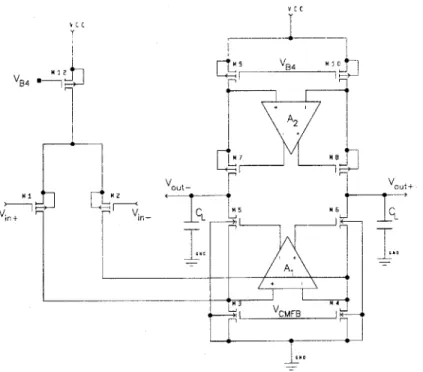
Another possible continuous-time CMFB circuit is shown in figure 2-10 [4, p.828].
Here, transistors MCM1 through MCM4 form two differential pairs that function as
the common mode detection network.
Figure 2-10 shows the CMFB amplifier. The folded-cascode op-amp is reproduced in Figure 2-11 as a reference to show the connections between the CMFB and the
op-amp. The v, and vcm, nodes are tied together. The CMFB circuit consists of
two differential pairs. The CMFB loop includes the differential pairs in the CMFB circuit as well as a portion of the main op-amp (the CMFB signal path goes through
V C C I DC I DC BIAS BIAS CM Detector VCM vIt. M C a MCM 2 M CII I__4 Vcm I MCM7 MCM5 NN C 6. IDC BIAS E4 C V out+ Figure 2-10: CMFB schematic.
transistors M3 - M6 in the main op-amp). Ignoring MCM7 and its current source
for now, each differential pair senses how far the positive or negative output has deviated from the desired common mode voltage and outputs a current proportional to this difference. The small-signal analysis below shows that the current fed back to the folded-cascode amplifier is a fraction of the difference between the average of the outputs and the desired common mode voltage. Note that Id, corresponds to the current through device M,.
IdCM2 -yncm2 baOP s VCM)
2 2
(2.21)
(2.22)
(The factor of 2 appears in the gmcm term because the effective transconductance
VB4 t FI V.in C C v B4 M0 V V ut+ LM out- V .,t F In Cl- C 82 <
r
M
AI
VMFigure 2-11: Folded-cascode schematic.
of a differential pair is 9.
IdCM5 = IdCM2 + IdCM3 = -Ibias - 2MCM ~ CM) (2.23)
With devices MCM1 through MCM4 sized equally, gmcm2 = gmcm3 =
9mcm-Analyzing the folded-cascode in Figure 2-11, the gain of the common mode-control
(from the gate of M3 to the output of the op-amp) is:
acmc= 9m3((/37ro9)//(05ro3)) (2.24)
Because this gain is derived from devices in the main op-amp, it remains the same regardless of the chosen CMFB topology. This gain is large enough so that the
com-mon mode sense gain from the gate of MCM2,3 to the gate/drain of MCM (acm,)
can be made to be small, which affords a larger bandwidth design. Without MCM7
acms = 2gmcm(9mcm6+9mcm7) , which is approximately a factor of 2 in gain improvement.
gmcm5gmcm6
Therefore the addition of MCM7 will give better control of the common mode output
with little added complexity. In both equations, gmcm is defined as the
transconduc-tance of MCM1, MCM2, MCM3, or MCM4 (which are all designed to match by
equal biasing and sizing).
The disadvantage of CMFB with two differential pairs is that the output swing of the op-amp is limited to the common mode differential input voltages that keep the differential pairs of the CMFB in the active region of operation. Writing KVL from
the gate of MCM1 to the gate of MCM2, and defining the common mode input as
Vid = Vut_ - VCM, we can calculate how much the output swing is limited by the
CMFB circuit:
2 1
BIAS
IA|
< W (2.25)To minimize the limitation that the CMFB circuit has on the output swing, we
can increase the bias current of the CMFB circuit, or decrease the 1 ratio of MCM1
through MCM4. For our application, I,,, = 200pA, yt,O ~ 38"A, and 1L = , so
we expect the input common mode range of the CMFB circuit to be: IVidl < 1.19V.
Determining the Optimal common mode Voltage
The output swing of the op-amp is effected by both the op-amp output stage and the CMFB input stage. Referring to Figure 2-1 for device names, one output reaches
its lowest limit (Vout,min) when transistors A13 and M5 or M4 and M6 exit saturation.
So Vout,min = 2VDS,SAT = 500mV, where VDSSAT has been approximated as 250mV.
The upper limit of one output (Vout,max) is reached when the input transistors of
the CMFB exit saturation. MCM1 -4 are operating in the active region when their
source-to-gate voltage VSG> Vtp- Plugging in VSG = VCC - VSD,SATO - Vout (where
VCC = 5V, VSD,SAT= 250mV, and V, = 0.95V) we find that Vout,max = 3.8V. To maximize the output swing, the common mode voltage should be halfway between
we can only expect for it to give us an approximate answer. In simulation, the actual optimal common mode voltage was found to be 2.25V.
Since Vout,max = 3.8V, and from Equation 2.25, we know that ividl 5 1.19V, the
CMFB circuit forces Vn,max equal to Vout,max - 2
Vid,max = 1.06V. Therefore, the
actual predicted single-sided swing of the op-amp is Vout,max - Vin,max = 2.74V. The
plot in Figure 2-23 shows the actual achieved output single-sided swing, which is ±1.43V from the common mode. The total differential swing is t2.86V, which meets our goal.
2.3
Gain-Enhancement through Active Cascoding
High open-loop gain is desirable in an op-amp because it affects the accuracy of the closed-loop network. Since our signal is important at frequencies between 8kHz and 25kHz, we want high open-loop gain at those frequencies. While a single stage folded-cascode amplifier is easily compensated (compensation is achieved by the output capacitance) and can have less noise and lower power than a multi-stage alternative, the DC open-loop gain is limited to ~50dB. Depending on the placement of the dominant pole, the gain at 20kHz can be equal to or less than 50dB. A technique called active cascoding can be used to increase the open-loop gain of the op-amp without adding extra stages.
2.3.1
Regular Cascode
This section will begin by reminding the reader of the regular cascode topology, and expand upon it by analyzing the active cascode and applying it to the folded-cascode op-amp analyzed in Section 2.1.
Small-Signal Analysis of a Standard Cascode
A typical two-transistor cascode structure is shown in Figure 2-12. Assuming the
output resistance of the current source bis, is very large, the small-signal DC gain of
vout
M 2
Vbis C
I
in
Figure 2-12: Cascode topology.
avd = -= gmiRout = gm19m2ro1ro2 = 13102 (2.26)
Vin
Note that cascoding increases the output impedance by the gmro of the cascoding transistor.
Noise of a Standard Cascode
Noise of the cascode circuit shown in Figure 2-12 is dominated by M1. M2 contributes
negligible noise because the current noise from M2 is proportional to its effective
transconductance, GM2, and its effective transconductance is small. Figure 2-13 shows
the models that we use to find the effective transconductance of M2. Intuitively, we
can look at M2 as being source degenerated by M1. From analysis on the small-signal
model in Figure 2-13(b):
GM2 9m2
gm2rol + 1
Therefore, the only important contributer of noise in the cascode circuit comes
V C C
I,
biasCu
M 21
Figure 2-13: Source degeneration
2.3.2
Basic Active Cascode Architecture
Active Cascode using an Op-Amp
Without adding extra stages, the easiest way to increase the gain of a folded-cascode amplifier is to add another level of cascoding. However, this cuts into an already limited signal swing. To increase the op-amp gain without reducing output swing, we can use the active cascode technique (also known as a regulated cascode) shown in Figure 2-14(a).
The amplifier with an open-loop gain of A(s) is called a gain enhancement amplifier and increases the gain of the cascode circuit by increasing its output impedance. The
gain enhancement amplifier sets the gate voltage of M2 such that the drain-to-source
voltage across M1 is held relatively constant despite changes in drain current, resulting
in a large output impedance. An analysis of the small signal model of the active cascode circuit, shown in Figure 2-14(b), shows that the active cascode increases the output impedance of the regular cascode by a factor of 1+A(s), where A(s) is defined
in Equation 2.29:
R = 32r01(1 + A(s)) = ,3r 1 s1 +A )(2.28)
V C C bias out-CL V + K IN bias (- -As) vL MI in s
(a) Active cascode topology.
vout
9m2V d (A(s)+1 0
gm1Vin r.,t
(b) Small signal model of the active cas-code.
Figure 2-14: Active cascode and its equivalent small signal model.
The open-loop gain of the gain enhancement amplifier A(s) is defined as:
A(s) A (2.29)
s-i + 1
In Equation 2.29, Ao is the open-loop DC gain of the active cascode amplifier,
and -L is the location of the dominant pole. The increased output impedance can beI
used to calculate the gain of the circuit:
avd = - = -gm, (Rout// 1 ) Pt
Vin sCL
f1 2(Ao + 1)(s 7"' + 1)
1 + s2roCL(Ao 0 + 1) + 82 32rol1CLT1
The second equality in Equation 2.30 arises from plugging in the result from
Equation 2.28 and assuming that r1 << 32rolCL(Ao + 1).
The transfer function for the active cascode circuit in Equation 2.30 shows that
there is a zero at z = A+1, which is also the unity gain frequency of amplifier
A. Using the approximations from Equation 2.8, we have a dominant pole at pi =
1 - and a second pole at P2 = -A0+1 Notice that zero z, and pole P2 appear
,32r0 CL A0 4
to cancel. However, remember this is only true if the approximation that we made
earlier holds: r << 02rlCL(A,+ 1). T1 is typically given by R',UtCL where R't is the
output resistance of the gain enhancement amplifier and CL' is its load capacitance.
Experimentation shows that sufficient cancellation is achieved for CL' = CL = 10pF.
An added benefit of a load capacitance placed at the output of the gain enhancement amplifier is that this capacitor also serves to compensate the active cascode feedback
loop.
The active cascode technique is limited by the bandwidth of the gain enhancement amplifier. This limitation reduces the usefulness of the technique for high-frequency applications. Fortunately, at our 8kHz to 25kHz frequency of interest, the active cascode technique does provide more gain boost than a standard cascode. At DC, the active cascode provides a much more substantial gain boost.
Single Transistor Gain Enhancement
L,, bicsl out bias2 MM3 Mn I in
Figure 2-15: Single transistor active cascoding.