Cylindrical Photonic Crystals
by
Mihai Ibanescu
Submitted to the Department of Physics
in partial fulfillment of the requirements for the degree of
Doctor of Philosophy in Physics
at the
MASSACHUSETTS INSTITUTE OF TECHNOLOGY
June 2005
©
Massachusetts Institute of Technology 2005. All rights reserved.
Author
...-.
Department of Physics
May 18, 2005
Certified
by...
I
....
...
John D. Joannopoulos
Francis Wright Davis Professor of Physics
Thesis Supervisor
- 11. A,
Accepted by...
... ... .. . .-- . e ...Th6mas J. 9ytak
Associate Department Head for E
cation
_ ,'- v,
OF TECHNOLOGY
JUN 07 2005
_ _
Cylindrical Photonic Crystals
by
Mihai Ibanescu
Submitted to the Department of Physics
on May 18, 2005, in partial fulfillment of the requirements for the degree of
Doctor of Philosophy in Physics
Abstract
In this thesis, we explore the properties of cylindrical photonic crystal waveguides in which light is confined laterally by the band gap of a cylindrically-layered photonic crystal. We show in particular that axially-uniform photonic band gap waveguides can exhibit novel behavior not encountered in their traditional index-guiding counterparts. Although the effects discussed in each chapter range from hollow-core transmission to zero and negative group velocity propagation and to high-Q cavity confinement, they are all a result of the photonic band gap guiding mechanism. The reflective cladding of the photonic crystal waveguide is unique in that it allows one to confine light in a low index of refraction region, and to work with guided modes whose dispersion relations lie above the light line of air, in a region where the longitudinal wave vector of the guided mode can approach zero.
Chapter 2 discusses hollow-core photonic band gap fibers that can transmit light with minimal losses by confining almost all of the electromagnetic energy to a hollow core and preventing it from entering the lossy dielectric cladding. These fibers have many similarities with hollow metallic waveguides, including the fact that they sup-port a non-degenerate low-loss annular-shaped mode. We also account for the main differences between metal waveguides and photonic band gap fibers with a simple model based on a single parameter, the phase shift upon reflection from the pho-tonic crystal cladding. In Chapter 3 we combine the best properties of all-dielectric and metallic waveguides to create an all-dielectric coaxial waveguide that supports a guided mode with properties similar to those of the transverse electromagnetic mode of a coaxial cable.
In Chapter 4, we introduce a mode-repulsion mechanism that can lead to anoma-lous dispersion relations, including extremely flattened dispersion relations, backward waves, and nonzero group velocity at zero longitudinal wave vector. The mechanism can be found in any axially-uniform reflective-cladding waveguide and originates in a mirror symmetry that exists only at zero longitudinal wave vector. In Chapter 5 we combine the anomalous dispersion relations discussed above with tunable waveguides to obtain new approaches for the time reversal (phase conjugation) and the time delay of light pulses.
Chapter 6 discusses a new mechanism for small-modal-volume high-Q cavities based on a zero group velocity waveguide mode. In a short piece of a uniform waveg-uide having a specially designed cross section, light is confined longitudinally by small group velocity propagation and transversely by a reflective cladding. The quality fac-tor Q is greatly enhanced by the small group velocity for a set of cavity lengths that are determined by the dispersion relation of the initial waveguide mode.
In Chapter 7, we present a surprising result concerning the strength of band gap confinement in a two-dimensional photonic crystal. We show that a saddle-point van Hove singularity in a band adjacent to a photonic crystal band gap can lead to photonic crystal structures that defy the conventional wisdom according to which the strongest band-gap confinement is found at frequencies near the midgap.
Thesis Supervisor: John D. Joannopoulos
Acknowledgments
I am very grateful to Professor John D. Joannopoulos who was a wonderful advisor and a good friend during the past six years and a half. His excellent teaching skills brought me closer to his research group. His guidance, support, and enthusiasm made research work seem like play. I want to thank him for giving me the chance to get involved in so many interesting projects and for reminding me how exciting the work we were doing was when sometimes I felt otherwise. Last, but not least, I would like to thank him for the many group parties he organized at his house, and to congratulate him for the exquisite cranberry sauce he prepares each Thanksgiving.
My fellow group members along the years each deserve a thank you for making this a special group. Thank you Alex, Ardavan, Aristeidis, Casey, Chiyan, David Chan, David Roundy, Evan, Jiang, Lefteris, Maksim, Marin, Matt, Michelle, Michael, Niko, Peter Bermel, Peter Bienstman, Shanhui, Steven, and Tairan. And for those who graduated before me, thank you for showing me that great opportunities lie ahead. Professor Yoel Fink deserves special thanks for his constant enthusiasm about our research and for helping bring many of our theoretical ideas closer to reality.
I want to thank my family for their trust in me when I decided to continue my education abroad and for the support they gave me over the years. I would also like to thank my girlfriend Simona for being a wonderful person and for her support during the sometimes difficult process of writing this thesis.
Contents
1 Introduction
1.1 Photonic Crystals and Photonic Band Gaps ... 1.2 Omnidirectional Reflectivity ...
1.3 Cylindrical Photonic Crystals ...
2 Hollow Cylindrical Photonic Band Gap Fibers
2.1 Introduction
.... .. . ... . .. . .. ... ... ... ..
2.2 Hollow Waveguides ...
2.3 Calculation of Modes of the OmniGuide fiber ...
2.4 Comparison of OmniGuide Fiber Modes and Metal Waveguide 2.5 Phase-Shift Model ...
2.6 Special Characteristics of the TEO1 Mode ...
2.7 Recent Experimental Developments ... 2.8 Conclusions ... 3 An 3.1 3.2 3.3 3.4 3.5 Modes . Modes
All-Dielectric Coaxial Waveguide
Introduction
...
From Metallic to All-Dielectric Waveguides . . Calculation of Coaxial Omniguide Modes .... Modes of Coaxial Omniguide A ...
Single-Mode Behavior in Coaxial Omniguide B
20 20 21 22 25 25 27 30 32 37 41 46 47 49 . . . . 49 . . . .52 . . . 56 . . . 58 . . . .60
3.6 Summary ...
4 Anomalous Dispersion Relations by Symmetry Breaking in Axially Uniform Waveguides 4.1 4.2 4.3 4.4 4.5 4.6
Introduction
... ...
Mode Symmetries in Axially Uniform Waveguides Mode Repulsion Caused by Symmetry Breaking . Anomalous Dispersion Relations ...Waveguide Designs ...
Summary
...
67 . . . .67 . . . .68 . . . .70 . . . .72 . . . .75 . . . .785 Phase Conjugation of Light Using a Negative Group Velocity Mode of an Axially-Uniform Waveguide 80
5.1 Introduction
. .... . . . ... . .. ... ... ... .. .... .. . 80
5.2 Phase Conjugation ... 82
5.3 Time delay ... 82
5.4 Summary ... 82
6 Microcavity Confinement Based on Anomalous Zero Waveguide Mode 6.1 Introduction ... 6.2 Zero Group Velocity at a Nonzero Longitudinal Wave 6.3 New Mechanism for Confining Light ... 6.4 All-Dielectric High-Q Cavity ... Group-Velocity 85 Vector Vector 85 86 89 90 6.5 Summary ...
... .
92
7 Enhanced Photonic Band-Gap Confinement via Van Hove Saddle
Point Singularities
95
7.1 Introduction . . . .. . . . 957.2 Evanescent Modes of the Bulk Photonic Crystal ... . 98
7.3 Enhanced Confinement via Saddle Point ... 99
7.4 General Arguments for the Existence of the Saddle Point ... . . 102
List of Figures
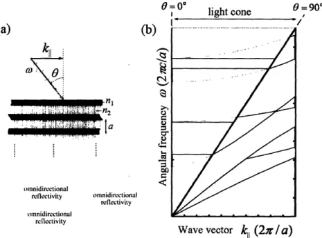
1-1 (a) Dielectric mirror made of alternating high and low index of refrac-tion layers. The incoming light is at an angular frequency w and has an angle of incidence 0. k is the component of the wave vector parallel to the air/mirror interface. (b) Projected band structure of the dielectric mirror. Light blue areas represent (, k1l) pairs for which
propagat-ing modes exist in the mirror. The yellow shaded area represents all frequency-wavevector combinations for which modes can propagate in air ( w > ckll) and is called the light cone. The two omnidirectional
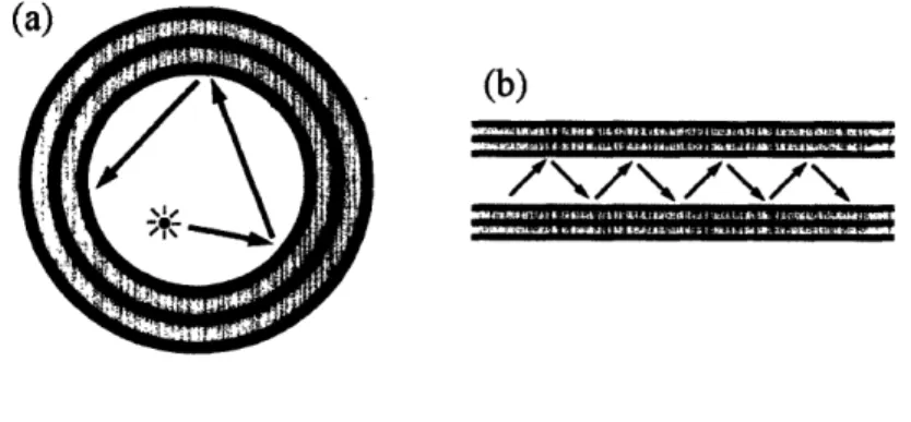
reflectivity ranges are shown in gray ... . 21 1-2 (a) A cylindrical waveguide is created by wrapping the omni-directional
mirror from Fig. 1-1(a) into a circle. Light is reflected by the mirror for any angle of incidence from air and thus has to propagate along the fiber as shown in part (b), which is a schematic longitudinal cross-section of the waveguide ... 22
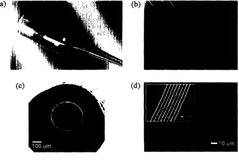
1-3 (a) Part of preform after it was heated and drawn into fiber. (b) Hundreds of meters of thin, flexible fiber are obtained from a single preform. (c) Cross-section of a hollow-core photonic band gap fiber with a diameter of about 700 1m. The multilayered dielectric mirror
can be seen as the thin lighter region immediately surrounding the core. (d) Magnified SEM of the hollow core, dielectric mirror, and polymer cladding. The inset shows the periodic arrangement of the chalcogenide and polymer layers. Imagescourtesy of Yoel Fink's group at MIT. . . 23
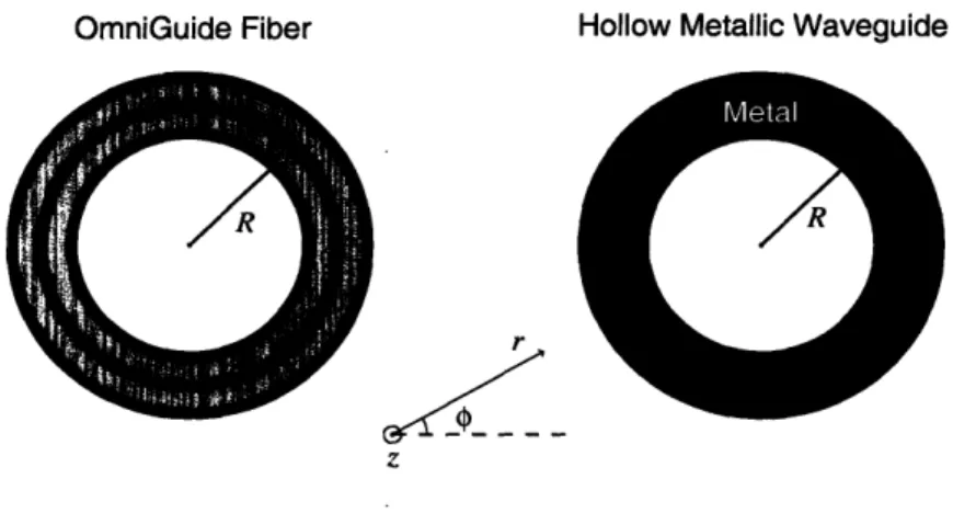
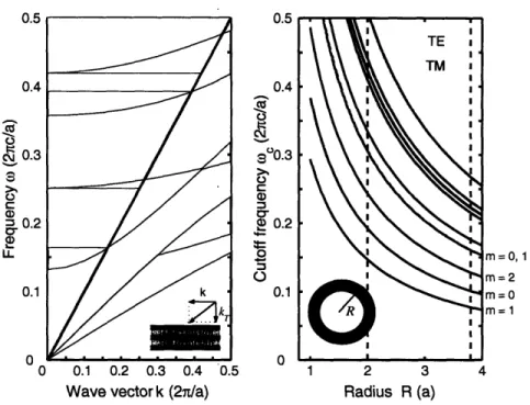
2-1 (Left) OmniGuide fiber of radius R. Light is confined in the hollow core by a multilayer dielectric mirror made of alternating layers with high (blue) and low (green) indices of refraction. (Right) Hollow metallic waveguide of radius R. Light is confined in the hollow core by a metallic cylinder ... 28 2-2 (Left) Projected band structure associated with the dielectric mirror.
The blue regions correspond to (k, w) pairs for which light can propa-gate through the mirror. The meaning of the parallel wave vector k is shown in the inset. kT is the transverse component of the wave vector. The diagonal black line represents the light line (w = ck). Shown in gray are two frequency ranges corresponding to omnidirectional reflec-tivity of the mirror. (Right) Frequency cutoffs of the lowest 11 modes supported by a hollow metallic waveguide are plotted versus the ra-dius of the waveguide. TE polarized modes are shown in red, while TM modes are shown in blue. The number m in the labels is the angu-lar momentum index of each mode. Note the degeneracy of the TE0, and the TM,1 modes. The two thick vertical dashed lines correspond
to radii R = 2.0a and R = 3.8a, which are the values used for the two exemplary waveguides considered here ... 29
2-3 Modes supported by an OmniGuide fiber of radius R = 2.0a are shown with solid lines. Red is for TE and HE modes, while blue is for TM and EH modes. Only the first three modes are labeled in each band gap. The lowest three modes in a hollow metallic waveguide with the same radius are plotted as dots ... 33 2-4 The lowest five modes supported by an OmniGuide fiber of radius
R = 3.8a are shown as solid red (TE or TE-like modes) and blue (TM
or TM-like modes) curves. Higher modes exist, but are not shown. . . 34 2-5 The electric-field time-average energy density for the five modes in
Fig. 4 is shown in a transverse cross section of the waveguide. The color scheme is such that the energy density goes from zero (black) to maximum (yellow). The thin blue contours represent the contours between the different layers of the OmniGuide fiber. For all five modes, the energy density is plotted for a frequency w = 0.230 (27r/a) ... 36 2-6 Combined phase shift and dispersion relation diagrams. Left panel:
contour lines for the phase shift, AqO, are plotted together with the band gap of the dielectric mirror (white region), and the light line (black oblique line). The modes of the OmniGuide fiber with R = 2.0a are shown as solid red/blue lines for TE/TM-like modes, while the modes in the metal waveguide are showed as dotted lines. The vertical arrows show the frequency difference between equivalent modes in the waveguides. The left and right panels are for modes with TE-like and TM-TE-like polarization, respectively. The crossing between the OmniGuide HE1l mode and the metallic TE1l1 mode is shown as a black
2-7 (Left) The confinement of electromagnetic energy in the hollow core of the OmniGuide fiber is plotted for three modes as a function of core radius. Actual data is shown as open circles. The solid lines represent fits as discussed in the text, and the dashed line is simply connecting the data points. (Right) The attenuation coefficient of the three modes is plotted as a function of radius. Also shown are the attenuation coefficient in silica fibers (0.2 dB/km) and a much larger attenuation coefficient (100 dB/km) assumed for the materials in the multilayer mirror. The circles and the lines have the same significance
as in the left panel ... 42
3-1 Schematics of coaxial waveguide cross sections: (a) traditional metallic coaxial cable; (b) coaxial omniguide, type A; and (c) coaxial omnigu-ide, type B. In parts (b) and (c), the gray layers represent cylindric dielectric layers, with dark gray corresponding to the high dielectric
constant material, and the light gray corresponding to the low
dielec-tric constant material. For all cases (a-c), light can be confined within the coaxial region, shown in yellow, and guided along the axial z-direction. In (a) and (b) the inner and outer radii of the coaxial region are ri = 3.00a and r = 4.67a, whereas in (c) ri = 0.40a and r = 1.40a. 53
3-2 Projected band structures along an axial direction. (a) Traditional metallic coaxial cable with inner and outer coaxial radii of ri = 3.00a and r = 4.67a, respectively. The red bands correspond to allowed guided modes. For any given wavevector, the lowest frequency mode is a TEM mode characterized by a perfectly linear dispersion relation. The six next highest bands correspond to transverse electric (TEml) modes with I = 1 and increasing angular momentum m. (b) Omni-directional, reflecting, all-dielectric multilayer film. Light-blue regions correspond to modes for which light is allowed to propagate within the dielectric mirror, and dark-blue regions correspond to modes for which light is forbidden to propagate within the dielectric mirror. The diago-nal black line identifies the edge of the light cone. The horizontal gray lines mark the boundaries in frequency within which omnidirectional reflectivity is possible. (c) Coaxial omniguide A with inner and outer coaxial radii of ri = 3.00a and r = 4.67a, respectively, and bilayers consisting of indexes of refraction n1 = 4.6 and n2 = 1.6 and thickness
d = 0.33a and d2 = 0.67a, respectively. The red and yellow bands
indicate guided modes confined to the coaxial region of the waveguide. The dashed lines indicate modes with less than 20% localization within the coaxial region. There is close correspondence between the modes labeled m = 1 to m = 6 and those of part (a) labeled TE11 to TE61.
Also, the yellow m = 0 mode corresponds to a TEM-like mode, as discussed in the text ... 54
3-3 Power density in the electric field for guided modes at kz = 0.19 (2r/a) in Fig. 3-2(c). Parts (a) through (d) correspond to guided modes with angular momenta m = 0 to m = 3, respectively. The color bar indi-cates that power increases in going from black to dark red, to red, to orange, to yellow. The blue circles identify the boundaries between the various dielectric shells and are included as a guide to the eye. Most of the power is confined to the coaxial region of the waveguide. The cylindrical symmetry and radial dependence of the m = 0 mode are consistent with those of a TEM mode. The small fluctuations in den-sity away from perfect cylindrical symmetry in (A) are a consequence
of the discrete square grid used in the computations ... . 59 3-4 Projected band structure for coaxial omniguide B. The central
dielec-tric rod has an index of refraction n = 4.6 and a radius ri = 0.40a. The coaxial waveguiding region has an outer radius r = 1.40a, and the parameters of the outer bilayers are the same as those used for config-uration A. The yellow dots represent confinement of the electric field power of more than 50%; the red dots represent confinement between 20 and 50%; and the dashed lines represent confinement less than 20%. The two white boxes identify the frequency ranges where the m = 0 band exhibits single-mode behavior ... 62
3-5 Electric field for the mode at frequency 0.203 (2zrc/a) and kz = 0.2 (27r/a) in Fig. 3-4. Parts (a) through (c) are the electric field components along the x, y, and z directions, respectively. The color bar indicates that large positive and negative values are shown as dark red and dark blue regions, respectively, whereas white areas represent regions of zero val-ues of the electric field, and light-colored areas represent regions of low values of the electric field. The field distribution clearly reveals a high confinement of the mode in the coaxial waveguiding region, and in this region it is nearly completely transverse to the direction of propagation
(less than 10- 3 of the intensity is along z), as desired ... 63
4-1 Top panel: Schematic drawings of the three types of reflective-cladding waveguides that employ metallic, multilayer-film, and photonic-crystal claddings. Bottom panel: Schematic band diagrams showing two neigh-boring modes as the relative frequency separation is decreased. At
k = 0 one mode is TE polarized and the other TM polarized (the
or-der is not important). (a) Weakly interacting modes. (b) A stronger interaction leads to a very flat lower band. (c) The repulsion between modes is strong enough to cause a backward wave region in the lower band. (d) Accidentally degenerate modes at k = 0 can have nonzero group velocity ... 69
4-2 (a) Dispersion relations of two modes with angular momentum unity for the cylindrical waveguide in inset. The dark regions have an in-dex of refraction 4.6 (e.g. Te), while the light gray regions have 1.4
(e.g. polymer). Starting from the center, the rod has a radius 0.45a,
the first ring has a thickness 0.32a, the second one 0.23a, and the fol-lowing low/high index layers have thickness 0.75a/O.25a, respectively. (b) Ultra-flattened dispersion relation in a photonic-crystal fiber with an index of refraction of 3.5 (e.g. semiconductor). The distance be-tween two neighboring air holes is a and the radius of a normal hole is 0.46a. The two dotted holes below the fiber core have a modified
radius of 0.40a . . . 76
5-1 Dispersion relations of the tunable waveguide for three values of the index of refraction of the central rod, n = 3.00, 3.15, and3.30. For wave vectors around 0.1 (27r/R) the group velocity can be changed from positive to zero and even negative values ... 81 5-2 The frequency spectrum of a pulse is flipped as a result of phase
con-jugation ... 83
6-1 Band structure of the axially-uniform dielectric-loaded metal waveg-uide (inset) showing the lowest two modes. The lower mode is anoma-lous with a non-trivial point of zero group velocity at k = 0.146 (27r/a), a = 0.1656 (27rc/a) ... . 87
6-2 (a) A piece of length L of the waveguide in Fig. 6-1 can form a high-Q cavity. (b) Resonant mode in cavity of length L = 3.9a. In an axial cross section, we show the electric field component perpendicular to the plane, with the red and blue regions corresponding to positive and negative values. The metal cladding is shown in black. Note that the
FDTD computational cell is actually larger than the rectangular box
shown here. (c) Resonant mode for L = 13.9a. (d) The quality factor Q is plotted as a function cavity length L. The red circles are the results of FDTD simulations, while the dashed vertical lines correspond to multiples of A/2. Also shown as a blue dashed line, is the Q(L) curve for a cavity based on a modified waveguide that does not have v = 0
at k # 0 ...
88
6-3 (a) A cylindrical all-dielectric cavity. (b) The axial cross section shows the cavity structure: on top of a substrate with refraction index nsub,
we have a central rod with index n followed by a region with index no and surrounded by a Bragg mirror that confines light to the core region. The electric field component perpendicular to the plane is shown in a
7-1 (a) A waveguide is formed by removing one row from a 2D square lat-tice of dielectric rods with refractive index 3.4 and radius r = 0.18a. (b) The dispersion relation of the waveguide mode (thick black line) is shown on top of a color contour plot of the confinement strength of the bulk photonic crystal (w, ki). The black regions include (, ki)
pairs for which propagating modes exist in the bulk crystal, while the colors from dark red to bright yellow, represent increasingly stronger confinement, as shown by the colorbar. (c) Confinement strength along the dispersion relation of the guided mode. The gray areas de-limit the complete band gap range. The y-axis is the same as in part (b) ... 97 7-2 The projected TM band structure of the bulk crystal is shown by the
blue areas and the black lines that represent w(k~) curves at constant ky values ranging from 0 to 0.5 (2r/a) in steps of 0.05 (27r/a). Note that the second band of bulk crystal has a saddle point singularity that is indicated by a thick black arrow. Also shown is the dispersion relation of the fundamental waveguide mode (red curve) ... . 99 7-3 Dispersion relations w(k(?) at fixed kx for propagating and evanescent
modes in the bulk crystal. The axial wave vector k takes the values 0, 0.2, 0.3, and 0.5 (2r/a) for parts (a) through (d). The imaginary part of k(n) is shown in red on the left side of each plot, while the real part is shown on the right, in blue for propagating modes and gray for evanescent and complex modes. In parts (a) and (c), the individual modes k(n) are labeled by the value of their n index. The A and B labels track the range of frequencies for which the n = 0 mode is evanescent, while the C label tracks the cutoff frequency of the n = -1 mode. . . 101
7-4 Contour plots of the second photonic crystal band w(kx, k) for varying radii of the dielectric rods: (a) r = 0 (vacuum), (b) r = 0.06a, (c) r = 0.12a, and (d) r = 0.18a. The same color scheme is used for all four parts of the figure. Constant-frequency contours are labelled by the corresponding value of the angular frequency w in units of (27rc/a). In parts (b), (c) and (d), a black dot indicates the position of the saddle point van Hove singularity ... 102
List of Tables
2.1 Summary of comparison between OmniGuide fiber (OGF) modes and their hollow metallic waveguide (HMW) counterparts. The first three modes are taken from Fig. 3 for a radius R = 2.0a, and the next two are from Fig. 4, corresponding to R = 3.8a ... 35
4.1 Possible Van Hove singularities in the density of states D(w) corre-sponding to the lower mode in Fig. 4-1(a-d) ... 74
Chapter 1
Introduction
1.1 Photonic Crystals and Photonic Band Gaps
Photonic crystals are periodic dielectric structures, with periodicity on the order of a wavelength, that alter the flow of light in ways not possible with traditional optical components [1, 2, 3, 4, 5]. The most dramatic behavior is found when the photonic crystal exhibits a complete band gap: a range of frequencies for which no propagating modes exist inside the crystal, and thus all incident light onto the crystal is reflected. This optical analogue to the electronic band gaps of semiconductors is very powerful as it allows for precise confinement and control of light inside photonic crystal devices such as cavities and waveguides. If spatial confinement in all three spatial directions is needed the perfect solution would be a photonic crystal with three-dimensional periodicity. Although continuous progress on such 3D crystals has been done in the past decade [6, 7, they are still rather difficult to fabricate. Self-assembly and holographic lithography techniques can lead to large volume bulk crystals, but don't allow for the easy introduction of useful defects. On the other hand, photo-lithography and e-beam lithography give control over the parameters of each unit cell, but become difficult to use if large volume 3D photonic crystals are required. In this thesis we
01 = light cone 0 90 (a) (b) > E 0^
e
omnidirectional reflectivity ominidirectional reflectivity omnidirctional reflcti'ity~refectivity Wave vector kll1(2r / a)
Figure 1-1: (a) Dielectric mirror made of alternating high and low index of refraction layers. The incoming light is at an angular frequency w and has an angle of incidence
0. kll is the component of the wave vector parallel to the air/mirror interface. (b)
Projected band structure of the dielectric mirror. Light blue areas represent (, k1l)
pairs for which propagating modes exist in the mirror. The yellow shaded area rep-resents all frequency-wavevector combinations for which modes can propagate in air ( w > ckll) and is called the light cone. The two omnidirectional reflectivity ranges are shown in gray.
focus on photonic crystal structures that are periodic in only one direction. Even though these structures cannot provide a complete photonic band gap, they still can lead to many interesting physical effects and useful photonic devices, as illustrated by the chapters of this thesis.
1.2 Omnidirectional Reflectivity
Key to the optical properties of one-dimensionally periodic photonic crystals is the concept of omnidirectional reflectivity. Consider the semi-infinite multi-layered di-electric mirror of Fig. 1-1(a), made of alternating layers with high and low indices of refraction. Incoming from the air above is light with an angular frequency w and
(b)
/ .../ a / \/\....' . Ti i'
/X/X//x,
Figure 1-2: (a) A cylindrical waveguide is created by wrapping the omni-directional mirror from Fig. 1-1(a) into a circle. Light is reflected by the mirror for any angle of incidence from air and thus has to propagate along the fiber as shown in part (b), which is a schematic longitudinal cross-section of the waveguide.
an angle of incidence . If there exists a frequency range in which light is reflected from the mirror for any angle of incidence 0 then we say that the mirror is an om-nidirectional reflector. For a long time, it was believed that such one-dimensional omnidirectional reflectors are not possible because one-dimensionally periodic struc-tures cannot have a complete photonic band gap. This can be understood with the help of Fig. 1-1(b) where we plot the w(k1i) band structure of the mirror, frequency
versus parallel wave vector. As can be seen, there is no frequency range without any propagating modes in the mirror. However, when we consider light that is incident from air onto the mirror, the parallel wave vector k is limited to be less than w/c, which is shown in Fig. 1-1(b) as the yellow-shaded region. Overlapping this allowed light cone region on top of the dielectric mirror band structures, we find that there exist indeed two frequency ranges shown in gray, for which the incoming light cannot couple to any propagating modes of the mirror, no matter what the angle of incidence.
1.3 Cylindrical Photonic Crystals
Cylindrical photonic band gap waveguides can be realized by simply taking a strip of the omnidirectional dielectric mirror and rolling it around into a cylinder as shown in
(b)
(c) (d)
Figure 1-3: (a) Part of preform after it was heated and drawn into fiber. (b) Hundreds of meters of thin, flexible fiber are obtained from a single preform. (c) Cross-section of a hollow-core photonic band gap fiber with a diameter of about 700 m. The multilayered dielectric mirror can be seen as the thin lighter region immediately sur-rounding the core. (d) Magnified SEM of the hollow core, dielectric mirror, and polymer cladding. The inset shows the periodic arrangement of the chalcogenide and polymer layers. Images courtesy of Yoel Fink's group at MIT.
Fig. 1-2. Light emitted inside of the waveguide or coupled into it cannot escape lat-erally because of the omnidirectional reflectivity properties of the cladding (coupling to cladding modes through evanescent tails is possible but limited to a narrow region near the cladding with a thickness comparable to a wavelength).
Before we move on to the various theoretical cylindrical photonic crystal designs of this thesis, it is important to mention that the first experimental steps towards actually implementing them in practice have already been taken. Fig. 1-3 describes the various steps involved in manufacturing a large-radius hollow-core photonic band gap fiber.
Chapter 2
Hollow Cylindrical Photonic Band
Gap Fibers
Preface
This chapter is based in part on Ref. [8]: M. Ibanescu, S. G. Johnson, M. Soljacic,
J. D. Joannopoulos, Y. Fink, O. Weisberg, T. D. Engeness, S. A. Jacobs, and M.
Sko-robogatiy, "Analysis of mode structure in hollow dielectric waveguide fibers," Phys.
Rev. E, vol. 67, 046608 (2003). We also discuss recent experimental implementations
of these fiber designs in Section 2.7.
2.1 Introduction
The advent of high-purity ultra-low-loss silica fiber as a transmission medium in the late 70's provided the basis for the modern optical communications infrastructure. Although highly successful, silica waveguides have fundamental limitations in their attenuation and non-linearities that result from the interaction of light with a dense, material-filled core. A different approach to waveguiding circumvents these problems by confining light in a hollow core using highly reflective walls. This approach is
exemplified by hollow metallic waveguides, which are very efficient in the millimeter wavelength range. Prior to the emergence of silica fiber, these waveguides were se-riously considered as candidate media for long-distance telecommunications [9]. An impairment of metallic waveguides is that they become lossy at high frequencies due to the finite conductivity of metals. Thus, their use is restricted to low frequencies and this severely limits the ultimate bandwidth that they can transmit. By adding a di-electric coating on the inside of the metallic waveguide one can improve its properties. Such metallo-dielectric waveguides have been developed for infrared wavelengths, in particular for laser power delivery [10, 11].
Here we analyze an OmniGuide fiber - a hollow all-dielectric waveguide in which light is confined by an omnidirectional mirror [12]. The limitations that exist in both the silica fiber and the hollow metal waveguides can be systematically reduced in this waveguide due to its hollow core and the use of dielectric materials transparent at high frequencies.
Yeh et al. showed in 1978 that it is possible to transmit a non-index-guided mode in a multilayer cylindrical dielectric waveguide [13]. The radiative decay of the mode is suppressed using a Bragg reflector, i.e. a multilayered structure that is periodic in the radial direction. Initial work in this area has focused on structures based on doped-silica technology that have a low index contrast between the layers [14, 15, 16, 17]. These structures are useful, for example, to control the dispersion parameter of a fiber in ways that are not achievable in a standard silica fiber [17]. However, such structures cannot confine light primarily in a hollow core because of the large penetration of the field into the low index-contrast multilayer structure. Recently, with the discovery of the omnidirectional high-reflectivity properties of multilayer films [18, 19, 20], researchers have focused instead on high index contrast dielectric waveguides [21, 22, 23, 24, 25, 12, 26]. Fink et al. fabricated a large-core high index-contrast hollow dielectric waveguide and demonstrated that light is transmitted even
when tight bends are introduced in the waveguide, a result of the omnidirectionality of the dielectric mirror [21]. Xu et al. developed an efficient analytical method for calculating approximate dispersion relations of the modes of such waveguides,
making use of the radial periodicity of the cladding layers [22]. Using this method, they calculated the number of layers required to suppress radiation as a function of the index contrast and substantiated that a large index contrast is necessary in order to limit the number of layers to a reasonable value [23]. Ibanescu et al. exploited the similarities between a dielectric multilayer mirror and a metal mirror and showed that it is possible to design an all-dielectric coaxial waveguide that supports a TEM-like
mode [25].
In this chapter, we study the properties of a hollow dielectric waveguide in which light is confined by a large index-contrast omnidirectional dielectric mirror. The large index contrast produces a high degree of optical confinement in the core and results in a waveguide mode structure that is very similar to the mode structure of a hollow metallic waveguide. We present the similarities and differences between the hollow dielectric and metallic waveguides, and explain these results using a single-parameter model based on the phase shift upon reflection from the dielectric mirror. In addition, we show that the similarities between these two types of waveguides extend to their transmission properties in that they have the same lowest-loss mode, the TEO1 mode.
2.2
Hollow Waveguides
The waveguides that we compare are shown in Fig. 2-1. On the left is depicted an OmniGuide fiber. A hollow core (index of refraction no = 1 ) is surrounded by an om-nidirectional mirror that consists of alternating layers having high and low indices of refraction [18]. The high/low index of refraction layers are shown in blue/green. The indices of refraction are 4.6/1.6 with corresponding thickness 0.33a/0.67a, where a is
Hollow Metallic Waveguide
r
Z
Figure 2-1: (Left) OmniGuide fiber of radius R. Light is confined in the hollow core by a multilayer dielectric mirror made of alternating layers with high (blue) and low (green) indices of refraction. (Right) Hollow metallic waveguide of radius R. Light is confined in the hollow core by a metallic cylinder.
the total thickness of a pair of layers. These values for the indices of refraction have been used in previous work [18, 21, 22, 23, 25, 12], including a fabricated multilayered waveguide operating at 10.6 ,m . The large index contrast between the two types of layers allows us to better illustrate the comparison between the hollow dielectric and metallic waveguides; the conclusions are still valid for a smaller index contrast that one may have to use in practice. In the frequency range of omnidirectionality of the dielectric mirror the similarities between the two types of waveguides are enhanced because, in both cases, the mirror that confines light in the core is a very good reflector
for all angles of incidence and polarizations. Moreover, the omnidirectionality of the
dielectric mirror is important for practical considerations: in an imperfect waveguide, the coupling between the operating core mode and cladding modes above the light line is eliminated if the frequency of operation lies in the omnidirectional frequency range of the mirror.
The exact value of a in microns is determined by the wavelength of operation of the waveguide. For example, if one wants to use A = 1.55/,m, then the thickness of a bilayer should be chosen somewhere in the range a = 0.3-0.4pm. The radius R of the waveguide will vary in the different examples presented in this chapter from a
0.5 0.4 0 o 0.3 v0.2 LSa C (D 0.1 n 0 0.1 0.2 0.3 0.4 0.5 0.4 0 14 C%" 3o0.3 On 0 C :, Cr . 0.2 0.1 n 0,1 2 0 1
Wave vector k (2l/a) Radius R (a)
Figure 2-2: (Left) Projected band structure associated with the dielectric mirror. The blue regions correspond to (k, w) pairs for which light can propagate through the mirror. The meaning of the parallel wave vector k is shown in the inset. kT
is the transverse component of the wave vector. The diagonal black line represents the light line (w = ck). Shown in gray are two frequency ranges corresponding to omnidirectional reflectivity of the mirror. (Right) Frequency cutoffs of the lowest 11 modes supported by a hollow metallic waveguide are plotted versus the radius of the waveguide. TE polarized modes are shown in red, while TM modes are shown in blue. The number m in the labels is the angular momentum index of each mode. Note the degeneracy of the TEO1 and the TM1l modes. The two thick vertical dashed lines
correspond to radii R = 2.0a and R = 3.8a, which are the values used for the two exemplary waveguides considered here.
minimum of 2a to a maximum of 20a.
On the right side of Fig. 2-1, we show a hollow metal waveguide. The core is the same as in the OmniGuide fiber (index of refraction 1, radius R), but a perfectly conducting metal cylinder now replaces the multilayer cladding.
We expect the multilayer structure to confine light in the core of the waveguide in a frequency range that corresponds to the band gap of a planar multilayer mirror having the same parameters as those of the multilayer structure in the waveguide. Indeed, it is precisely in this band-gap region that we expect the mode structure of
the OmniGuide fiber to resemble that of a hollow metal waveguide.
In the left panel of Fig. 2-2, we plot the projected band structure for a planar multilayer dielectric mirror for which the layers have the same indices of refraction and the same thicknesses as those of the layers present in the waveguide. If w is the angular frequency of an incoming plane wave and k is the component of the wave vector parallel to the mirror, then regions in the (k, w) plane shown in blue correspond to plane waves that can couple to propagating modes in the mirror and are transmitted through the mirror. The two gray areas in the plot correspond to the omnidirectional frequency ranges of the dielectric mirror. For these frequencies, light cannot be transmitted through the mirror for any angle of incidence of a plane wave incoming from the outside air region. Both the TE and TM polarizations are overlapped in the plot.
In the right panel of Fig. 2-2, the frequency cutoffs of the lowest 11 modes sup-ported by a hollow metallic waveguide are plotted versus the radius of the waveguide. The dispersion relation of a mode with cutoff frequency wc is given by w2- c2k2+ wC.
TE polarized modes are shown in red, while TM modes are shown in blue. The num-ber m in the labels is the "angular momentum" and describes the azimuthal symmetry of each mode. Note the degeneracy of the TEO1 and the TM1l modes (4th and 5th
modes).
2.3 Calculation of Modes of the OmniGuide fiber
We calculate the modes supported by the OmniGuide fiber using the transfer-matrix method. As in any waveguide with cylindrical symmetry, there are three useful con-served quantities: w, the frequency, k, the wave vector in the axial direction, and m, the angular momentum (m = 0, 1, 2, ... ). The general form of the z component of the electric field, Ez, in the i-th layer of the structure for a mode with wave vector k
and angular momentum m is:
Ez(z, r, = [)
[A
Jm(kT,ir) + Bi Ym(kT,ir)]- (2.1).ei(kz-wt) eimO,
where Ai and Bi are coefficients that vary from layer to layer, J and Y are Bessel functions, and kT,i is the transverse wave vector, kT,i = (niw/c)2 - k2. Hz is given
by a similar expression, but with different coefficients Ci and Di. From the Ez and Hz components one can calculate all the other components of the electromagnetic field components [27]. The coefficients in the (i+l)th layer are related to those in the i-th layer by a 4-by-4 transfer matrix, such that the boundary conditions are satisfied [13]. The last step before finding the modes is to establish boundary conditions at the outside surface of the outermost layer. Here we require that the incoming radial electromagnetic flux be zero, which corresponds to the physical situation in which the sources of electromagnetic field are only inside the waveguide [12]. The solutions that we obtain with this boundary condition are guided modes (with real wave vectors) and leaky modes (with complex wave vectors).
The OmniGuide fiber supports modes that are analogous to the guided modes of a hollow metallic waveguide. These modes are resonant modes that have most of their energy traveling in the hollow core. Their field decays exponentially in the radial direction in the dielectric layers. These modes have (k, w) pairs situated in the band gap of the dielectric mirror and above the light line. The wave vector k has an imaginary part that is proportional to the radiative loss of the modes. This imaginary part decreases exponentially with the number of layers in the dielectric mirror; in the limit of an infinite number of layers these resonant modes become truly guided modes. For the dielectric mirror with only five layers shown in Fig. 2-1, the imaginary part is on the order of 0- 4 .27r/a. This means that light can be confined in the hollow core for a distance equal to several hundred wavelengths before it radiates
away. For a waveguide intended for transmission of light over longer distances, more layers need to be added to the cladding. Fortunately, the imaginary part of the wave vector decreases exponentially with the increase in the number of layers. Thus, for pure TE modes, only 20 layers are enough to give radiative decay lengths of more than a hundred kilometers, while for TM modes and mixed modes, 40 layers are enough. For a detailed analysis of radiation suppression see [23, 12].
The OmniGuide fiber also supports other categories of modes. One category includes modes that are index guided in the dielectric mirror. In Fig. 2-2, these modes are situated below the light line, in the light-blue regions of the w(k) diagram. Their field decays exponentially in the air regions, but extends throughout the dielectric mirror. Another category includes modes that decay both in the air regions and in the dielectric layers. These only exist as surface states between the core and the multilayer cladding. (They can also be found deeper into the multilayer structure if a defect is introduced by altering the thickness or the index of refraction of one or more layers). In Fig. 2-2, these modes are situated below the light line in the band gap of the dielectric mirror.
2.4 Comparison of OmniGuide Fiber Modes and Metal
Waveguide Modes
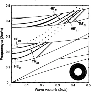
In Fig. 2-3, we show the lowest-frequency resonant modes of the OmniGuide fiber for a radius R = 2.0a. TE modes and TE-like (HE) modes are shown as solid red lines, while TM and TM-like (EH) modes are shown as solid blue lines. The modes of a hollow metallic waveguide with the same radius are shown as dots. The Figure shows that, indeed, the dispersion relations of the OmniGuide fiber are very similar to those of the metallic waveguide, but the modes can now only exist in the TE or TM band gaps of the multilayer mirror. For example, the TM01 mode in the metallic
0.5 0.4 cN 0.3 e-a) ' 0.2 0r U_ 0.1 n 0 0.1 0.2 0.3 0.4 0.5
Wave vector k (27/a)
Figure 2-3: Modes supported by an OmniGuide fiber of radius R = 2.0a are shown with solid lines. Red is for TE and HE modes, while blue is for TM and EH modes. Only the first three modes are labeled in each band gap. The lowest three modes in a hollow metallic waveguide with the same radius are plotted as dots.
0 a cm a, U-0 0.05 0.1 0.15 0.2 0.25 0.3
Wave vector k (27/a)
Figure 2-4: The lowest five modes supported by an OmniGuide fiber of radius R =
3.8a are shown as solid red (TE or TE-like modes) and blue (TM or TM-like modes) curves. Higher modes exist, but are not shown.
waveguide (blue dots) is now split into two sub-modes, TM01 and TM'1. Thus, it is
useful, in a zeroth order approximation, to think that the dispersion relations for the different modes of the OmniGuide fibers can be obtained by overlapping the band structure of the dielectric mirror on top of the dispersion relations for the metallic waveguide. Finally, we note that it is possible for resonant modes to exist outside the omnidirectional frequency range (such as the HE1 mode for k < 0.05 (27r/a) in
Fig. 2-3) as long as the modes fall within the band gap.
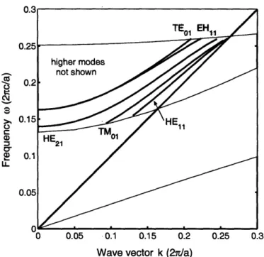
In Fig. 2-4, we show the dispersion relations for a larger radius of the fiber,
R = 3.8a. More resonant modes can be found now in the first band gap, as the
cutoff frequencies vary inversely with the radius R. We focus on the first band gap of the dielectric mirror, and we consider only the lowest five resonant modes of the waveguide.
Mode label Cutoff frequency Degeneracy OGF HMW OGF HMW Diff. OGF HMW
HE1 1 TE1 1 0.155 0.146 +6% 2 2
TMo1 TMo1 0.189 0.191 -1% 1 1
HE2 1 TE2 1 0.223 0.243 -8% 2 2
EH11l TM11l 0.163 0.160 +2% 2 2 TEo1 TEo1 0.163 0.160 +2% 1 1
Table 2.1: Summary of comparison between OmniGuide fiber (OGF) modes and their hollow metallic waveguide (HMW) counterparts. The first three modes are taken from Fig. 3 for a radius R = 2.0a, and the next two are from Fig. 4, corresponding to
R = 3.8a.
in metal waveguides of corresponding radii (R = 2.0a and R = 3.8a). In particular, we will compare the resonant modes to the metal waveguide modes in terms of their cut-off frequencies, group velocities, group velocity dispersions, degeneracies and mode symmetries. The lowest resonant mode in Fig. 2-3 is HE11, with a cutoff frequency
w = 0.155 (27r/a) . This corresponds to TE11, the fundamental mode in a hollow
metal waveguide, which has a cutoff at w = 0.146 (27r/a). The second mode in Fig. 2-3 is TM0 1 with w = 0.189 (27r/a), corresponding to TMo0 1 in the metal waveguide
with w = 0.191 (2r/a). Note that for m = 0 modes, the OmniGuide fiber modes are exactly TE or TM polarized, as is the case with all metal waveguide modes. For non-zero m, TE modes become HE modes, and TM modes become EH modes. Also, in both waveguides, the non-zero m modes are doubly degenerate, while the m = 0 are non-degenerate.
In Table 1, we summarize the similarities between the equivalent modes in the OmniGuide fiber and the hollow metallic waveguide. The first three modes are taken from Fig. 2-3 for a radius R = 2.0a, and the next two are from Fig. 2-4, corresponding to R = 3.8a. The cutoff frequencies for the two types of waveguides are quite similar for all the five modes. The differences vary from -8% for the HE21 mode, to +6% for
the TMo01 mode. Note also that modes that in the metal waveguide have low cutoff
TM01
EH1 1 TEo1
0 max
Figure 2-5: The electric-field time-average energy density for the five modes in Fig. 4 is shown in a transverse cross section of the waveguide. The color scheme is such that the energy density goes from zero (black) to maximum (yellow). The thin blue contours represent the contours between the different layers of the OmniGuide fiber. For all five modes, the energy density is plotted for a frequency W = 0.230 (2w7r/a).
modes with higher cutoff frequencies are shifted down. This effect will be explained later in terms of the phase shift of the dielectric mirror.
The group velocity of a resonant mode is zero at k = 0 and approaches c as the frequency is increased, as is the case in a metal waveguide. However, as the mode nears the upper band edge, the group velocity starts decreasing as a result of the gradual loss of confinement in the core.
The group velocity dispersion of a resonant mode is positive for low frequencies (closer to the lower edge of the band gap), negative for high frequencies and transitions through zero. This is in contrast to the group velocity dispersion of modes in a metal waveguide, which is always positive.
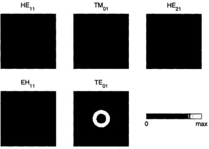
To provide a better understanding of the field patterns of OmniGuide fiber modes, in Fig. 2-5 the electric-field time-average energy density 2
E
is plotted for the fivemodes shown in Fig. 2-4 at a frequency w = 0.230 (2r/a). All modes are normalized such that the power flowing in the z direction is the same. Also, in order to capture
the angular dependence of a mode, we no longer use the eimo complex form of the field. Instead, we use linear combinations of the degenerate m and -m modes to obtain real fields.
All modes appear to be very well confined to the hollow core. The energy density in the cladding layers is much smaller than the energy density in the core, which is why the cladding layers appear dark in the Figure. The TEO1 mode is different
from the other four modes in that its electric field energy density has a node near the core-mirror interface. This is true in general for all modes of the same symmetry, i.e. TEoe with
e
= 1, 2, .... Note that the number of angular oscillations of the energy density is twice the angular momentum of a mode.In order to quantify the comparison between the field distribution of modes in the OmniGuide fiber and in the metal waveguide we use a correlation function F defined
by:
=
|rdrdqEl(r,
f_
q) . 4 1/2 (2.2)[f
rdrdo E1(r,0)
2 f rdrd E2(r,0)
2]P can take values in the interval 0, 1], a value of 1 corresponding to maximum correlation ( = 1 can only happen if the two modes are the same up to a constant amplitude scaling factor). For all modes, the correlation is largest close to the middle of the band gap and decreases as the mode approaches the band edges. The maximum value of the correlation as a function of frequency is above 95% for all modes, and the largest correlation is found for the TEO1 mode: 99.1%.
2.5 Phase-Shift Model
In both the hollow metallic waveguide and the OmniGuide fiber, light is confined in the air region because it is reflected back to the core by a cladding: a metal wall in
the first case and a dielectric multilayer film in the second. Thus, it is convenient to analyze the differences between the modes in the two waveguides in terms of the different reflection properties of the two mirrors. Since the reflectivity is very close to 100% in both cases, the important difference between the two mirrors is found in the phase shift AOb acquired by an electromagnetic wave upon reflection. For the TE polarization, this phase shift is defined by:
-= ei (2.3)
Eli
where Ell and Ell are the tangential components of the electric field for the incident and reflected waves respectively. In the above formula, we assume that the reflectivity is 100%, which is true for a perfectly conducting wall and is a very good approximation for a dielectric mirror with a large enough number of layers. For a metallic mirror, AOb is always equal to 7r because the tangential electric fields of the incident and reflected waves have to cancel. For the TM polarization we calculate AO in a similar manner,
using the tangential components of the magnetic field this time: Hll/Hll =-ei ac .
With this definition, AOb for a metal mirror is equal to r for all polarizations and angles of incidence.
In Fig. 2-6 we plot the phase shift of the dielectric mirror as contours on a plot which includes the band gap edges, the light line, and dispersion relations for the fiber with R = 2.0a. The phase shift is a function of w and k, or, equivalently, of the frequency and the angle of incidence. Also, it is a function of the polarization of the incident wave. For both polarizations, we can identify a = 7r line near the center of the band gap (shown with a thicker black line). This is where we expect the dielectric mirror to be most similar to a metal mirror. The other contour lines correspond to phase shifts of 1.17r, 1.2r,... for increasing frequencies, and 0.91r, 0.87r,... for decreasing frequencies. The qualitative difference between the two polarizations is that for the TE polarization the phase shift at a given frequency approaches 7r near
0 0.1 0.2 0.3 0 0.1 0.2 0.3 Wave vector k (27/a) Wave vector k (27/a)
Figure 2-6: Combined phase shift and dispersion relation diagrams. Left panel: con-tour lines for the phase shift, A\q, are plotted together with the band gap of the dielectric mirror (white region), and the light line (black oblique line). The modes of the OmniGuide fiber with R = 2.0a are shown as solid red/blue lines for TE/TM-like modes, while the modes in the metal waveguide are showed as dotted lines. The vertical arrows show the frequency difference between equivalent modes in the waveg-uides. The left and right panels are for modes with TE-like and TM-like polarization, respectively. The crossing between the OmniGuide HEl mode and the metallic TE11
mode is shown as a black dot.
the light line, whereas for the TM polarization it varies substantially near the light line.
Also shown in Fig. 2-6 are the confined modes for the metallic waveguide (dashed lines) and for the OmniGuide fiber (solid lines). On the left, we present TE-like modes while on the right the pure TM mode is shown.
As seen in Fig. 2-6, the difference in the dispersion curves for the confined modes in the metallic waveguide and the OmniGuide fiber are correlated with the difference in phase shifts between the dielectric and metal mirrors. In particular, the following observations can be made:
The point of crossing between the mode and the metallic TE1l1 mode lies very
close to the A = w7r line.
(ii) The frequency distance between the equivalent modes in the metal and
from AO = 7r.
(iii) The confined modes in the dielectric waveguide are drawn towards the A\ = 7r line when compared with the modes confined in the metal waveguide.
Next we present a simple model that explains qualitatively the above observations by relating the phase shift to the dispersion curves. We approximate the transverse field profile of a confined mode of the OmniGuide fiber by a standing wave between two planar walls separated by the diameter of the waveguide. The total phase ac-quired by a wave that traverses the waveguide diameter twice has contributions from propagation over a distance 2 (2R) and from two reflections upon the mirror. Thus,
AStotal = 4kTR +
2AOb,
(2.4)
where kT is the transverse wave vector of the mode in core. The condition for a standing wave is that this phase must equal a multiple of 27r: A\(total = 2ir. This in
turn leads to the approximate dependence of the transverse wave vector on the phase shift:
kT = (fr - ZAO)/(2R).
(2.5)
Calculating kT from this equation should be done self-consistently because AO is a function of w and k, and therefore a function of kT.
From Eq. (2.5) we see why the phase shift AOb has important effects on the dis-persion relations of modes. Since kT is a decreasing function of AO, and because
w2/c2 = k2 + k2, it follows that an increase in the phase shift AO will cause a
de-crease of the frequency w of a mode at a fixed wave vector k. This result explains the three qualitative observations made above about the OmniGuide modes when compared to the metallic waveguide modes.
the OmniGuide modes are pulled inside the band gap when compared to their metal-lic counterparts. This is entirely due to the fact that the phase shift increases with increasing frequency. One consequence is that the group velocity of the OmniGuide modes is always slightly smaller than that of the corresponding metallic modes. It is interesting to imagine what would happen if one could design a multilayer dielectric mirror for which the phase shift decreased with increasing frequency: in such a waveg-uide, the modes would be pulled out towards the band-gap edges, leading to modes with larger group velocities which could approach the upper bound of c. However, it is an empirical law that the phase shift always has the general behavior shown in Fig. 2-6. Finally, we note that the point of maximum correlation between OmniGuide fiber modes and metallic modes, as defined above, occurs very close to the AO = 7r line.
2.6 Special Characteristics of the TE
01
Mode
For practical applications, it is of interest to identify the losses associated with the different modes of the waveguide. Metallic waveguides were the subject of intensive research aimed at utilizing them for long distance optical communications. It was found that the TE0 1 mode is the lowest loss mode in a metal waveguide, due to the presence of a node in the electric field at the metallic wall. This mode was the operating mode for the long distance communication lines designed by the Bell Laboratories prior to the advent of silica fibers [9]. In the remaining portion of chapter, we will examine some of the properties of the TE0 1 mode in the OmniGuide
fiber; these properties were studied in more detail in [12].
In the left panel of Fig. 2-7, we plot the confinement in percent of the electromag-netic energy in the core for the TE0 1, TM0o1, and HE11 modes as a function of the
O 0 8 3 .o0 M -c.B 0 Z) 0) C n la 01) 10 'ayer::::: : ::::::::::::::: s ... :. ... : :. .-
~~~~~~
... ... ..... :::::::::::.::::::::::::::::::::.:: 1 .. ...1
... E~~~~H... . ...1... I TM: ... 01 : . : :::::::::::::::::::::::::::::::::::,:::::;:: 10 ... ... 0 . .-:: : : .-:: : : : .-::: : : : : : : : : : : ::: : : ::.: : : : : : : : ... ... O ... ... ... ... co ~1-1 ~10 -.... . . . ... ... .. . . .. 5 10 15 20 3 5 10 15 20Radius R (a) Radius R (a)
Figure 2-7: (Left) The confinement of electromagnetic energy in the hollow core of the OmniGuide fiber is plotted for three modes as a function of core radius. Actual data is shown as open circles. The solid lines represent fits as discussed in the text, and the dashed line is simply connecting the data points. (Right) The attenuation coefficient of the three modes is plotted as a function of radius. Also shown are the attenuation coefficient in silica fibers (0.2 dB/km) and a much larger attenuation coefficient (100 dB/km) assumed for the materials in the multilayer mirror. The circles and the lines have the same significance as in the left panel.
the largest confinement for all values of R. Furthermore, its confinement in the core approaches 100% at a faster rate then the other modes. The penetration of the TE0,
field into the multilayer structure is very well approximated by a 1/R3 dependence.
We will present a justification for the 1/R3 dependence below. A fit to the actual data points (open circles) is shown in Fig. 2-7 as a solid red line. The TM01 confinement
approaches 100% at a much lower rate. A fit with a 1/R3 dependence is shown as
a solid blue line. The HE1 mode has a mixed polarization and has a more complex
variation with the core radius. However, the rate at which its confinement approaches 100% is less than that of the TE01 mode.
In the right panel of Fig. 2-7, we plot the attenuation coefficient caused by dissi-pation losses for the three modes. (We assume the dielectric mirror has enough layers such that the radiation losses are negligible). We assume the core of the waveguide is lossless, while the materials in the dielectric mirror have a dissipation coefficient of 100 dB/km (chosen to much larger than the loss of silica). Even with such lossy materials in the dielectric mirror, the loss of the TEO1 mode is smaller than the loss
of silica fibers (0.2 dB/km) if the core radius R is larger than approximately 8a. This is because the dissipation loss for TEo ( = 1, 2, ... ) modes decreases as 1/R3. This
general result is a consequence of the presence of a node in the electric field near the core-mirror interface, as will be shown below. Note that while the silica fiber has a very low loss only for wavelengths near A = 1.55/,m, the OmniGuide fiber can be designed to have a very low loss in the vicinity of any desired wavelength, from infrared to visible wavelengths.
The 1/R3 dependence of the TE01 dissipation loss is due to the presence of a node
in the electric field of this mode near the interface between the hollow core and the first layer of the dielectric mirror. The only non-zero component of the electric field for the TE0 1 mode is E. In the case of a metallic waveguide, this component would
of the dielectric waveguide, the node in Es is found very close to the interface. To get an estimate of the dissipation losses, we take the ratio of the power that travels in the layers to the total power carried by the mode. A more precise expression
is derived in [12], but the proof of the 1/R3 dependence is the same. Let Acore be
the amplitude of the electric field in the core, and Alayers the amplitude in the layers. The area of the core is rR2. Because of the exponential radial decay induced by the
band gap, the power in the layers is found mostly in the first few layers, in an area approximately equal to 27rR dp (dp is the penetration depth of the field into the layers and is independent of R). With these notations, the estimate for the loss coefficient
is:
Los ayers Alayers2 (2.6)
A2o core ' ~RIT 2 R Acore
where we kept only terms that influence the R dependence.
Because of the small amplitude of Es, at the core-layers interface, it is the derivative of Es, with respect to r that connects the amplitudes Alayers and Acore. If we
approxi-mate the radial field oscillations by sinusoidal oscillations, the derivative of Es close to
a node is given by the transverse wave vector times the amplitude of Ed. Thus, the am-plitudes in the core and in the layers are connected by kT,coreAcore - kT,ltayersAT,Itayers.
The transverse wave vector kT,core is inversely proportional to R, because the TE0,
mode always has half an oscillation of E, between the origin and r = R. In a layer with index of refraction n, we have kT = (nw/c)2- k2. As R becomes larger, the
TE0 1 mode will get closer to the light line, and therefore k approaches w/c. If n is not
equal to 1, kT will be almost independent of R. Thus kT,layers is almost independent of R. Thus, we have
Alayers kTcore (2.7)