HAL Id: hal-00661342
https://hal.archives-ouvertes.fr/hal-00661342
Submitted on 19 Jan 2012
HAL is a multi-disciplinary open access
archive for the deposit and dissemination of
sci-entific research documents, whether they are
pub-lished or not. The documents may come from
teaching and research institutions in France or
abroad, or from public or private research centers.
L’archive ouverte pluridisciplinaire HAL, est
destinée au dépôt et à la diffusion de documents
scientifiques de niveau recherche, publiés ou non,
émanant des établissements d’enseignement et de
recherche français ou étrangers, des laboratoires
publics ou privés.
Imagery of local defects in multilayer components by
short coherence length interferometry
Laurent Vabre, Vincent Loriette, Arnaud Dubois, Julien Moreau, A.C.
Boccara
To cite this version:
Laurent Vabre, Vincent Loriette, Arnaud Dubois, Julien Moreau, A.C. Boccara. Imagery of local
defects in multilayer components by short coherence length interferometry. Optics Letters, Optical
Society of America - OSA Publishing, 2002, 27 (21), pp.1899-1901. �10.1364/OL.27.001899�.
�hal-00661342�
November 1, 2002 / Vol. 27, No. 21 / OPTICS LETTERS 1899
Imagery of local defects in multilayer components by short
coherence length interferometry
L. Vabre, V. Loriette, A. Dubois, J. Moreau, and A. C. Boccara
Laboratoire d’Optique Physique, Centre National de la Recherche Scientifique, Unité Propre de Recherche A0005, Ecole Supérieure de Physique et de Chimie Industrielles, 10 rue Vauquelin, 75005 Paris, France
Received April 22, 2002
We propose to image local defects inside multidielectric optical components by using a special configuration Linnik interference microscope, along with a CCD camera and a dedicated detection, to extract the amplitude scattered by the defects in the interference image. The use of a short coherence length source allows one to obtain interference only from a thin slice共⬃1 mm兲 within the observed object. The object is tilted to permit the use of a dark-field configuration to enhance the defect contrast. We describe the experimental setup and the detection scheme. Images that exhibit local point defects on the interfaces of various multilayer optical components (laser mirrors) are presented. © 2002 Optical Society of America
OCIS codes: 180.3170, 110.4500, 220.4840.
Some thin-f ilm research has been directed toward improving the quality of multilayer coatings. Stan-dard control techniques, such as ellipsometry and scatterometry,1
provide powerful means for evaluating coating performance. However, these methods are inappropriate for the detection and study of pointlike defects inside buried structures. Inasmuch as point defects are usually the major sources of scattering in high-quality components, it is thus a crucial task to quantify the inf luence of such local defects on the structure of the coating and on its local characteristics. The main challenge is to obtain local information from a single buried interface of the component without physical contact with the component. This procedure would be particularly interesting at the end of the fab-rication process, when the whole multilayer structure is present.
Phase measurement interferometry is a powerful method for obtaining surface prof iles with nanometric resolution.2,3
However, in the case of multilayer com-ponents, such measurements are made with diff iculty because the optical phase is integrated along the optical path through several layers. The apparent measured topography of a buried interface is a combi-nation of the true topography and the topography of the layers located above it. The result is not simply a sum, because the incident wave front is not parallel to the observed surfaces; so obtaining the real to-pographies will require complex operations. To avoid this problem we propose to work with the interference signal’s amplitude rather than with its phase. To en-hance the contrast of this method, we use a dark-f ield configuration to avoid specular ref lection on the interfaces.
The use of a short coherence length source enables one to obtain interference only from a thin slice. Use of this method is well known for the investigation of biological tissues (it is called the optical coherence tomography technique)4
and for volume reconstruc-tion.5,6
Here we propose to apply this principle to
imaging the local defects of the interfaces inside a multidielectric structure.
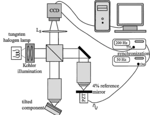
The experimental setup is depicted in Fig. 1. It is based on a home-built Linnik interferometer.7
The Linnik conf iguration is more useful than the Mi-rau configuration, for example, for choosing the reference mirror and permitting the use of large-numerical-aperture objectives. As the amplitude of the light scattered by the local defects is weak, we use a low-ref lectivity reference mirror 共Rref 苷 4%兲 to increase the contrast of the interference signal. The light source is a broadband tungsten halogen lamp that provides a coherence length close to 2.6 mm at a central wavelength of l0 苷 800 nm (axial resolution,
LC兾2 苷 1.3 mm). The interference signal is detected
by a dedicated multiplexed lock-in detection scheme that was described previously.8
The interference
Fig. 1. Schematic representation of our Linnik inter-ference microscope. Phase modulation is achieved by a piezoelectric transducer (PZT) synchronized with image acquisition by means of the two generators. LS is a lens
that enables the objectives to work in inf inite conjugation. TTL, transistor – transistor logic; Out, sinusoidal signal driving the PZT.
1900 OPTICS LETTERS / Vol. 27, No. 21 / November 1, 2002
Fig. 2. Schematic of the dark-f ield conf iguration. The object is tilted to eliminate specular ref lection. We obtain one echo per interface. LC is the coherence length of the
light source 共LC兾2 1.3 mm兲.
Fig. 3. Images of a multidielectric component. (a) Image before the limit angle. We can clearly observe one inter-ferogram per interface. Some large defects have already been revealed. (b) Image in the dark-f ield conf iguration. No interferogram is visible. Point defects are well defined on the various interfaces. Exposure time, 2 s. Field of view, 380 mm 3 380 mm.
image is digitized on a CCD array (256 3 256 pixels, 8 bits). To perform lock-in detection we introduce periodic phase modulation into the interference signal by means of a PZT that is sinusoidally modulated at frequency f兾4, where f 苷 200 Hz is the camera’s frame rate. We then record four frames during each modulation period. As was previously demonstrated,8 the amplitude of the interference can be calculated from these four integrated values.
Our aim is to observe the local defects on the inter-faces, but light that is due to the specular ref lection on these interfaces (a few percent) will mask the signal induced by such defects (a few parts in 106). For that reason we adopted a dark-f ield configuration to eliminate the specular ref lection of the interfaces. Interference is produced between light ref lected by the reference mirror and light scattered by the local de-fects. To obtain a dark-field configuration we tilted the multilayer component (see Fig. 2). With that configuration, we obtained different responses, each corresponding to an inteferogram for an interfaces.
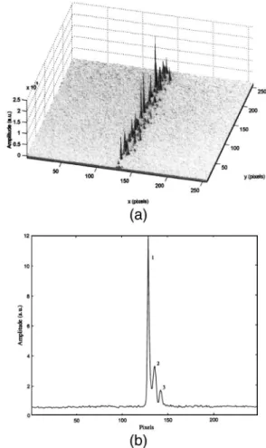
Figure 3(a) shows the four responses from the four interfaces of a low-quality multidielectric component (two sequences of SiO2兾Ta2O5) when the component was tilted before the dark-f ield limit. Figure 3(b) shows the same area tilted after the dark-f ield limit. We observe only the signal that is due to local defects whose locations are apparent. Figure 4(a) shows the response of a three-layer CO2 laser mirror recorded in a dark-field conf iguration. Figure 4(b) shows the sum of the amplitude values along the direction of the fringes共y兲, where one peak per interface is observed.
We are able to detect an image of the defects, but the remaining diff iculty is in calibrating the measure-ments to determine the sizes of the defects. We are not able to quantify our measurements yet. However, we can estimate the sensitivity limit of our setup. We found that, when the signal is integrated for less than a few seconds (a few hundreds of images) the main noise source is shot noise. For longer integration times, technical noises become dominant (thermal and mechanical drifts). We previously demonstrated8 that the lowest equivalent sample ref lectance Rmin that can be detected by our technique is
Fig. 4. (a) Response of a CO2 laser mirror. Three
interfaces with various local defects have been detected. (b) Sum of the pixel values along the direction of the fringes (column). Three peaks, corresponding to three interfaces, are apparent. Exposure time, 2 s. Field of view, 380 mm 3 380 mm.
November 1, 2002 / Vol. 27, No. 21 / OPTICS LETTERS 1901
Fig. 5. Radius of the smallest detectable particle as a function of the number of sequences acquired (1 sequence苷 total exposure time 4兾f ⬃ 0.02 s). These values were obtained by use of Mie scattering theory; a spherical air bubble inside a silica substrate is assumed.
Rmin苷 共R
ref1 2Rinc兲2
N jmaxRref
, (1)
where Rincis the part of the incoherent light backscat-tered on the CCD, N is the number of summed images (representing exposure time t苷 4N兾f), and jmaxis the number of photoelectrons per pixel required for satura-tion (the data sheet gives jmax苷 120, 000 for our CCD camera). The lowest equivalent sample ref lectance is
Rmin⬃ 3 3 1027 for a single measurement (exposure time, 10 ms). Using a simple Mie scattering model9 of an air bubble 共np 苷 1兲 trapped inside a silica sub-strate共nm苷 1.45兲, we can estimate the size fminof the smallest detectable defect. The results of the numeri-cal numeri-calculation are shown in Fig. 5 as a function of the number N of acquired sequences. When one averages 100 sequences (2 s), 23-nm-radius particles should be detected. An expression approaching fmincan be de-rived, where fmin,, l0:
fmin苷 ∑ 3 4 µ l p ∂4 Rmin np Ç m21 2 m22 1 Ç2
3共4 2 3 cos umax2 cos3umax兲21 ∏1兾6
, (2)
where np is the refractive index of the trapped par-ticle, m苷 np兾nm, where nmis the material’s refractive index, and umax is the apparent aperture angle, which depends on nmand on the numerical aperture of the ob-jectives. The sensitivity could be further improved by use of objectives with larger numerical apertures and also by shifting of the average incident wavelength to-ward the blue region of the spectrum [Eq. (2)]. The next step is to obtain a complete image, not only a line, of point defects on a particular interface. This could be done in one of several ways, such as simply by trans-lating the sample along the z axis and recording the lines to build the full image.
The authors are grateful to V. Reita and P. Piart for mechanical conception and realization. L. Vabre is grateful to the Délégation Générale pour l’Armement for f inancial support. This work is supported by the Centre National de la Recherche Scientif ique (France). L. Vabre’s e-mail address is [email protected].
References
1. J. S. Stover, Optical Scattering: Measurements and Analysis, 2nd ed. (SPIE Press, Bellingham, Wash.,
1995), Chap. 6.
2. K. Creath, Prog. Opt. 26, 349 –393 (1988).
3. S. S. C. Chim and G. S. Kino, Appl. Opt. 30, 2197 (1991). 4. D. Huang, E. A. Swanson, C. P. Lin, J. S. Schuman, W. G. Stinson, W. Chang, M. R. Hee, T. Flotte, K. Gre-gory, C. A. Puliaf ito, and F. G. Fujimoto, Science 254, 1178 (1991).
5. P. A. Flourney, R. W. McClure, and J. C. Wyntjes, Appl. Opt. 11, 1907 (1972).
6. A. Harasaki, J. Schmit, and J. C. Wyant, Appl. Opt. 39, 2107 (2000).
7. L. Vabre, A. Dubois, and A. C. Boccara, Opt. Lett. 27, 530 (2002).
8. A. Dubois, L. Vabre, A. C. Boccara, and E. Beaurepaire, Appl. Opt. 41, 805 (2002).
9. C. F. Bohren and D. R. Huffman, Absorption and
Scat-tering of Light by Small Particles (Wiley Interscience,