J.B. Ve´chembre and G.R. Foxa)
Laboratoire de Ce´ramique, Ecole Polytechnique Fe´de´rale de Lausanne, Lausanne, Switzerland CH-1015
(Received 5 May 1998; accepted 5 January 2001)
Pt electrodes with a 6–8-m thickness were produced on alumina substrates by a double-print Pt screen-printing process that included a sequential heat treatment at 600 °C and 1300 °C. This process improved the final sintered double-print film because the first printed layer acted as a sintering template for the second printed layer. The sintered Pt films have a 95% coverage of the alumina surface, 92% density, 0.73-m average surface roughness, and 16.10−5⍀ cm resistivity. The sintering behavior of Pt films exhibited three stages of densification: Stage I (T °C < 700 °C), exhibiting neck growth, and Stage II (700 < T °C < 1300 °C), exhibiting grain growth, have activation energies of 64 kJ/mol and 125 kJ/mol, respectively. Stage III exhibits a decrease in shrinkage due to Pt coalescence and island formation. The transition temperature, 700 °C, between Stages I and II corresponds to an anomalous increase in surface roughness and resistivity. The thickness of Pt films was a critical parameter for achieving alumina surface coverage. Uniaxial pressing of dried Pt films increased densification and reduced the surface roughness of double-print Pt films.
I. INTRODUCTION
Piezoelectric PbZrxTi1−xO3(PZT) thick films prepared by screen printing are increasingly being studied to re-alize microelectromechanical devices for a variety of sensor and actuator applications.1–5 Examples of such devices include micromotors,6,7ultrasonic transducers,8,9 pressure sensors,10 –15 and micropositioners. Screen-printing technology for the fabrication of PZT thick films is of industrial interest due to its possibility for produc-tion of relatively low-cost films with thickness between 5 and 100m.16–19 Many microelectromechanical de-vices require thin piezoelectric layers <100m in thick-ness. In comparison, machining of bulk ceramics is costly for the 5–100-m thickness range, and thin-film processes are generally limited to thickness of <5m. Screen-printing processes for PZT coatings are not only promising because of the thickness range that is attain-able but also because films can be directly patterned during the printing process with line widths as small as 10m.20 The versatility, reproducibility, and relatively low cost of screen printing has been demonstrated in a variety of electronic materials,16,18,19,21but the technique has not been fully exploited to fill the gap between bulk ceramic and thin-film processing of PZT.
Piezoelectric thick-film devices are effectively capaci-tor structures that require high-quality electrodes for ef-ficient operation. Initial efforts for device development are being placed on building electrode/PZT/electrode multilayer structures or capacitor stacks on Al2O3 sub-strates. This work focuses on the fabrication of continu-ous Pt bottom electrode coatings deposited by screen printing. A continuous Pt bottom electrode is not only needed for efficient electrical performance but is also needed for a reaction barrier between the PZT and the Al2O3 substrate.22,23 Thermal stability and surface smoothness of the electrode surface are also critical for subsequent processing of the PZT layer. In our experi-ence, the bottom electrode must remain stable to tem-peratures >1000 °C, i.e., the electrode must not become discontinuous during PZT thick-film sintering because the Pt layer blocks Pb and Al diffusion during PZT sin-tering.24,25Pb from the PZT reacts with Al2O3 to form Pb2Al2O5and also interdiffuses with intergranular amor-phous phases within the ceramic substrate.24 The diffu-sion of Al from the substrate into the PZT has also been observed, and this causes the formation of second phases.25This type of reaction between the substrate and PZT alters the PZT electrical behavior. In addition to the reaction barrier performance of the bottom electrode dur-ing PZT processdur-ing, the bottom electrode must maintain a smooth surface to avoid problems with short circuits between top and bottom electrodes.
a)
Present address: Ramtron International Corporation, 1850 Ram-tron Drive, Colorado Springs, CO 80921.
Screen printing of inks containing conductive fillers is widely used for fabrication of thick-film electrode such as Pt and resistor coatings.18,19,26 Most of these inks consist of glass frit, conductor particles, and an organic vehicle. The glass frit improves adhesion between the conducting phase and the alumina substrate after the sin-tering process.18,19,26 However, the glass resides at the interface between the conductive particles of the conduc-tor layer and the substrate; the glass can migrate through the grain boundaries of the conductive particles during sin-tering, resulting in glass at the surface of the conductive layer.27Glass at the surface of the conductive coating can react with subsequently deposited layers that are either co-fired with the primary conductive coating or co-fired in a sepa-rate sintering process.27,28 With PZT thick-film devices, glass frit contained in the electrode ink can have detrimental effects on the PZT properties. In addition, the glass frit remaining in the grain boundaries of the electrode coating will reduce the conductivity of the electrode compared with a coating consisting purely of the conductive phase.
To avoid the problems associated with glass frit con-taining electrode inks, pure platinum ink was chosen for fabrication of the bottom electrode for PZT thick films. The platinum is known to remain chemically inert during PZT sintering at high temperature22and to be an effec-tive diffusion barrier between PZT and Al2O3.
23 How-ever, previous work has indicated that platinum may not exhibit sufficient thermal stability on alumina sub-strates29,30because Pt is inclined to form a discontinuous electrode consisting of interconnected platinum islands and holes extending through the entire Pt film thickness during sintering at high temperatures. This phenomenon can occur when the ratio of the average Pt grain size to Pt film thickness reaches a critical value.30
The objective of this study was to determine proc-essing conditions of screen-printed Pt thick films that would result in continuous, smooth platinum coatings on alumina substrates while avoiding problems of Pt island formation that results in holes in the Pt film. A set of tests were conducted to determine how sintering temperature, heating rate, Pt film thickness (i.e., number of screen-printed layers) and uniaxial pressing of screen-printed and dried films influenced the constrained sintering of screen-printed Pt films. Both microstructure and sheet resistance analyses were used to identify the most appropriate processing con-ditions of Pt films for application to subsequent PZT thick-film processing. These studies also provided insight to the basic phenomenon controlling the densification and surface coverage of screen-printed Pt films on alumina.
II. EXPERIMENTAL PROCEDURE
Pure Pt ink (FERRO, E-1189, San Marcos, CA) was used for screen printing onto 99.6% alumina substrates (Coors, Superstrate). The Pt ink consisted of 65% (by
weight) flake Pt particles with an average gain size of 3m, whereas the remaining 35% of the ink constituents were organics. The alumina substrates had dimensions of 51 × 51 × 0.38 mm, a grain size of <1m, and a surface roughness of 50 nm. A DEK screen printer mounted with a hard, square squeegee was operated with a squeegee blade speed of 10 cm/s for deposition of Pt films onto the alumina substrates. The Pt ink was printed through a 400-mesh stainless steel screen consisting of 18-m diameter wires with a weave pattern fixed at 45° with respect to the rigid aluminum frame and the direction of motion for the squeegee. The screen contained 34–
42-m holes with 51% open area. A 13-42-m-thick emulsion
defined the 27 × 27-mm pattern, which resulted in the same size prints of Pt films on the substrates.
After printing, the Pt films were left undisturbed for 15 min to allow reflow of the ink, which reduced the film surface roughness produced by the screen mesh. The films were then dried at 120 °C for 15 min to remove the organic solvents from the film. The densification, surface coverage, and surface roughness of the Pt films were studied as a function of temperature, heating rate, film thickness, and uniaxial pressure applied to dried Pt films. Samples were heated in a box furnace to temperatures ranging between 300 and 1350 °C to determine how the organics burn out and densification proceeds during sin-tering. Heating rates of 2 and 5 °C/min were studied. The sintering of as-dried films was compared with dried films that were uniaxially pressed between polished alumina blocks at a pressure of 165 MPa. Pt films prepared by using a single-print process exhibited as-dried thickness of 10–11m and sintered thickness of 4–5 m under optimum firing conditions. These films were compared with thicker films that were deposited by a double-print process. In the double-print process, each layer was se-quentially printed and dried, and after drying the second layer, the double-print film was uniaxially pressed. In an alternative double-print process, each layer was dried, pressed, and fired sequentially. Thickness of the dried double-layer films were 18–20m, and the fired thick-ness was between 6 and 8m.
Thickness measurements of the Pt films were made by using a profilometer (TENCOR Alpha Step 200) (Kla-Tencor, San Jóse, CA). Twelve thickness measurements, three on each side of the printed square, were used to de-termine the average film thickness as well as monitor thick-ness gradients in dried and sintered films. The platinum layer thickness was measured after three of the processing steps: drying, uniaxial pressing, and sintering. From these measurements, the thickness shrinkage was determined be-tween the three processing steps by using the relation
Shrinkage⳱ {Ti− Tp(or Ts)}/Ti .
where Ti, Tp, and Ts are the initial, pressed, and sintered thickness, respectively.
The microstructures of the resulting films were observed with a Philips XLF-30 (Eindhoven, The Netherlands) scan-ning electron microscope (SEM). Plan-view surface images of samples were used to verify the surface coverage and the continuity of the platinum thick films as well as determine Pt grain sizes. Cross sections were prepared by breaking samples. The cross-sectional views show the volume den-sity of platinum layers and give information about the shape of the platinum grains and surface roughness.
A laser microfocus measurement system (UBM Messtechnik GMBH, Germany) was used for roughness measurements of the platinum films. The instrument uses a focused infrared laser beam to interrogate the sample surface and create quantitative 3-D images that give a measure of the surface roughness. The measurements were realized on bare substrate and platinum thick-film surfaces of 1 × 1 mm2. For the Pt thick films, a roughness map of the surface was taken from the center of a printed square. Two parameters Raand Rpmwere chosen to char-acterize surface roughness. Ra is the arithmetic average of the absolute values of all points of the profile; Rpmis the arithmetic average of the Rpvalues of five consecu-tive sections each of equal length, where Rpis the maxi-mum height of a profile peak relative to the mean line for the entire measurement trace. Ragives a measure of the average surface roughness, whereas Rpm gives informa-tion about the height of the largest surface features. This latter measurement is relevant to the relationship be-tween surface roughness and short circuits in certain ca-pacitor structures formed with the Pt films. Sheet resistance measurements of the Pt films were made with a four-point probe measurement technique, and the bulk resistivity was determined from the sheet resistance and the thickness of the films.
III. RESULTS AND DISCUSSION A. Single-Print Platinum Coatings
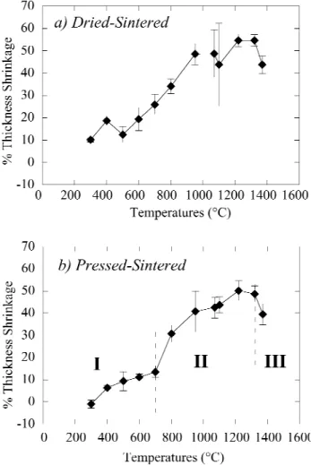
The densification of single-print films was first studied by observing the temperature dependence of Pt film thickness shrinkage as shown in Fig. 1. The details of experiments are indexed in Table 1. Figure 1(a) shows the shrinkage between dried and sintered films, whereas Fig. 1(b) gives the shrinkage curve between the uniaxi-ally pressed and sintered states. It is clearly seen that uniaxial pressing reduces the variance in the shrinkage results probably due to improvements in film green den-sity. The effects of uniaxial pressing will be discussed in more detail in Sec. III. B. Even with the large experimen-tal errors in Fig. 1(a), it can be seen that both sintering curves differ from the monotonic sintering curves usually observed for bulk metal powder compacts because the temperature dependence of Pt film shrinkage consists of three distinct stages. The three stages are more discern-ible in Fig. 1(b), which shows the shrinkage for pressed
films. Between 200 and 700 °C (Stage I), the shrinkage between the pressed and sintered state increases asymp-totically toward a value of approximately 15%. At tem-peratures >700 °C, the slope of the shrinkage curve increases dramatically and then begins to level off, re-sulting in a shrinkage maximum of 50% at 1200 to 1300 °C (Stage II). At temperatures >1300 °C, there is an obvious decrease in shrinkage (Stage III).
Assuming that the sintering and associated shrinkage is controlled by lattice diffusion31–34 as described by Eq. (1),35activation energies (E
a) for Stages I and II can be calculated from the slope of a plot of ln(T2/5⌬t/tp) versus 1/T (Fig. 2). ⌬t tp =A× D*2Ⲑ5 T2Ⲑ5 where D*=D0×exp
冉
− Ea RT冊
, (1) where A ⳱ constant; ⌬t ⳱ change in thickness, tp ⳱ pressed thickness, D0 ⳱ diffusion coefficient, andT⳱ absolute temperature.
FIG. 1. Temperature dependence of thickness shrinkage between (a) dried and sintered and (b) uniaxially pressed (165 MPa) and sintered states of single-print Pt thick films.
Stages I and II exhibit activation energies of 64 ± 4 and 125 ± 13 kJ/mol, respectively. In comparison, the densification of bulk pure metal powder compacts can be represented by a single straight-line plot from which a single activation energy of 270 kJ/mol is obtained.29,36,37 The two distinct stages of densification for Pt thick films may arise because of the influence of carbon impurities on Pt diffusion at low temperatures or changes in the dominant diffusion mechanisms for the two temperature ranges. The platinum ink contains organic solvents and binders that evaporate and burn out at temperatures <200 °C as confirmed by the thermal gravimetric analy-sis in Fig. 3. However, carbon residues often remain in materials to temperatures as high as 700 °C. These car-bon residues can influence the Pt diffusion at low tem-peratures.38 Because the Pt film is constrained by the underlying substrate, it can be expected that shrinkage will not exhibit the same temperature behavior as ob-served for bulk materials. Densification across the thick-ness of the film is expected to occur at a different rate than densification within the film plane because of physi-cal and chemiphysi-cal interactions between the thick film par-ticles and the substrate.29 It is expected that the two densification behaviors will exhibit different temperature dependencies, thus providing a possible explanation for the two-stage shrinkage curves. Additional experiments
are required to determine whether the two activation en-ergies are a result of impurities or constrained sintering of thick films.
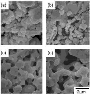
SEM micrographs of the film microstructures give ad-ditional insight to the densification process occurring during sintering. Figure 4(a)–(c) shows the microstruc-ture of an as-dried Pt film and progressive neck forma-tion between Pt particles for sintering in Stage I. For temperatures up to 700 °C, the Pt particles densify lo-cally to form grains or dense clusters of grains that form a porous skeletal network. Although the pore chan-nels seem to be continuous, the diameter of the pore channels seems to be smaller than the thickness of the
TABLE I. Shrinkage between dried and sintered thickness, and pressed and sintered thickness of platinum layers at different firing temperatures for single-print platinum coatings.
Sample Temperatures (°C) % Dried-sintered % Pressed-sintered Error 1 300 10.071 −1.071 Single sample 2 400 18.711 6.307 Single sample 3 500 12.512 9.332 Single sample 4 600 16.078 11.874 5 600 24.095 10.045 6 600 19.403 11.184 7 600 21.806 5.4588 8 600 24.352 10.121 Average 600 21.15 9.74 1.25 9 700 20 13.01 10 700 26.68 15.094 11 700 25.42 12 700 26.14 14.624 13 700 26.443 13.563 Average 700 24.937 14.073 0.551 14 800 34.155 29.9 15 800 28.482 16 800 32.995 30.11 Average 800 33.575 29.497 0.626 17 950 48.51 40.741 Single 18 1070 48.743 42.468 Single 19 1100 52.65 43.753 Single 20 1220 54.644 50.158 Single 21 1300 54.699 48.684 Single 22 1320 54.693 48.673 Single 23 1370 43.753 39.544 Single
FIG. 2. Activation energy plot.
FIG. 3. TGA showing weight loss due to pyrolysis of organic com-ponents of the platinum ink.
film, and direct pathways to the substrate surface are not observed. Necking between the Pt particles proceeds in all three dimensions. Above 700 °C, in Stage II [Fig. 4(d) and 5(a)–(c)], the skeletal Pt network seems to col-lapse and densify resulting in larger, locally densified regions and enlarged pores that have diameters that are approximately the same size as the thickness of the film and that extend directly through the entire thickness of
the film. This process of local densification with elimi-nation of small pores and enlargement of larger pores continues up to 1300 °C. Above 1300 °C, in Stage III, the locally densified Pt islands continue to coalesce and be-come more spherical in shape [Fig. 5(d) and Fig. 6]. Al-though the Pt islands still exhibit a significant connectivity, the coalescence, or balling-up, of these is-lands is believed to be the reason for a decrease in thick-ness shrinkage in Stage III. The coalescence increases the spherical size of the Pt grains to the detriment of alumina coverage. When profilometer thickness measurements are made on the Pt layers, the holes in the Pt layer are not taken into account because the diameter of the stylus tip (25m) is larger than the film pore size. As a result, for Stage III films, the measured sintered thickness seems to increase with coalescence of Pt islands and a correspond-ing growth of grains to a size that is equal to or greater than the thickness of the film. It should be noted that in contrast to Stage I, the densification processes for Stages II and III are limited to two dimensions because most pores extend through the film thickness. The ob-served sintering behavior suggests that single-print films with thicknesses that are approximately equal to the Pt grain size cannot be sintered to provide sufficient sub-strate coverage for electrode applications.
FIG. 4. SEM surface images showing the microstructural evolution of (a) an as-dried single-print Pt layer and single-print films sintered at (b) 400 °C (Stage I), (c) 700 °C (transition from Stage I to Stage II), and (d) 800 °C (Stage II) for 18 min with a heating rate of 2 °C/min.
FIG. 6. SEM (a) cross-sectional image and (b) oblique image at the border of the Pt pattern showing sphereodization of Pt grains after sintering at 800 °C for 18 min with a heating rate of 2 °C/min. FIG. 5. SEM surface images showing the microstructural evolution of
single-print Pt layers sintered at (a) 800 °C (Stage II), (b) 1050 °C (Stage II), (c) 1300 °C (transition from Stage II to Stage III) and (d) 1350 °C (Stage III) for 18 min with a 2 °C/min heating rate.
B. Double-Print Platinum Coatings
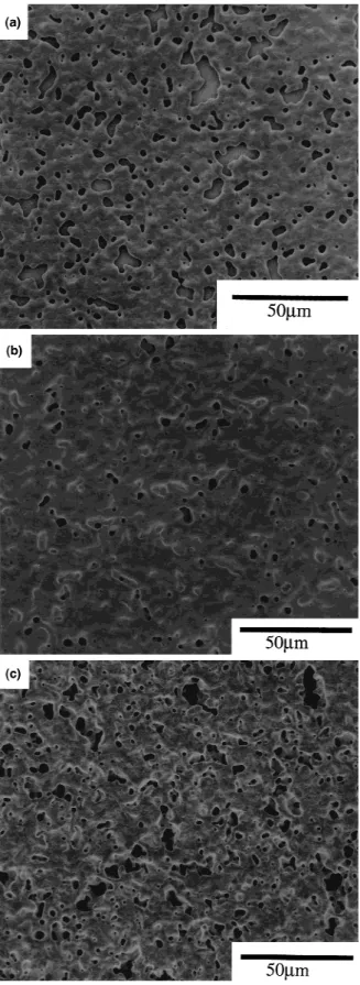
Because of the limited substrate coverage obtained with single-print Pt coatings, double-print coatings were investigated in an attempt to improve alumina surface coverage. Figure 7 shows the microstructures for a single- [Fig. 7(a)] and double- [Fig. 7(b)] print film with the same sintering profile. The increased Pt thickness for the double-print films results in a reduced con-centration of pores that cause exposure of the alumina surface. This result supports the conclusion that there is a critical thickness that exists for the formation of continuous Pt films that provide complete coverage of the alumina surface.30This critical thickness depends on Pt grain size and the interfacial energy between the Pt and the alumina. Because both the stability of Pt par-ticles and the interfacial energy depend on tempera-ture, the energetically stable critical thickness of the film is also a function of temperature. To determine whether double-print films were sufficiently thick for both alumina coverage and thermal stability, a series of experiments were completed to determine sintering pro-files that lead to densification without Pt coalescence and island formation that results in incomplete coverage of the alumina.
It was first observed that the heating rate had a sig-nificant influence on the surface coverage of the alumina. Increasing the heating rate from 2 to 5 °C/min leads to an increase in Pt pore size and open area of the alumina as shown in Fig. 7(c). The influence of heating rate on alumina surface coverage indicates that the Pt densifica-tion depends on diffusion and reacdensifica-tion processes (such as binder burnout and interfacial reactions between the Pt and alumina) occurring in both temperature regimens of sintering (Stages I and II). Slower heating rates, which translate into longer dwell times within Stage I, increase surface coverage, suggesting that longer dwell times in the Stage I temperature regimen are advantageous for obtaining alumina coverage. Because the pathway for densification is obviously important, it is clear that densification processes in both sintering stages need to be optimized to obtain further improvements in alumina surface coverage and densification of double-print Pt films.
For double-print films, it can also be expected that the path by which the individual printed layers are densified (i.e., optimization of Stages I and II sintering) will strongly influence the Pt film microstructure and alumina surface coverage. To test this hypothesis, a range of tem-peratures between 400 and 1300 °C were used as a first anneal of just the first layer of double-print films, and then the films were refired at 1300 °C after printing the second layer. The SEM images in Fig. 8 show a distinct improvement of the alumina coverage for these sequen-tially sintered bilayer films in comparison with bilayer films that underwent only a single heat treatment (Fig. 7).
FIG. 7. SEM surface images showing the difference in alumina sur-face coverage for (a) single-print films (4.3m sintered thickness) and (b) double-print films (6.0m sintered thickness) sintered with a heat-ing rate of 2 °C/min, and (c) double-print films (8.0m sintered thick-ness) sintered with a heating rate of 5 °C/min. All films were annealed at 1300 °C with an 18-min hold time.
All firing temperatures between 400 and 1300 °C for the first printed layer, followed by a second firing at 1300 °C after deposition of the second layer, resulted in improved alumina coverage for double-print films. At low first an-nealing temperatures, 400–500 °C, a relatively high den-sity of small pores (2m in diameter at 400 °C) remains after the second firing. When the first annealing tempera-ture increases, the pore size increases and the pore den-sity decreases, resulting in an optimum alumina surface coverage of >95% at 600–700 < (Table 2). At first an-nealing temperatures >700 °C, the pores continue to in-crease in size and the pore density also inin-creases, resulting in reduced alumina surface coverage.
To determine whether the alumina surface coverage measurement could be used as a direct measurement of the density of the film, F, the density was calculated from the mass of the Pt film after sintering, mPt, the thickness of the Pt film after sintering, TPt,S, and the printed area. The density was calculated by using the following formula:
F⳱ mPt/(2.7 cm)(2.7 cm)TtPt,S .
The alumina surface coverage for the film sintered at 600 and 1300 °C, respectively, for the first and second heat treatments, exhibited an alumina surface coverage of 97%, whereas the density was found to be only 77% of the theoretical density of Pt. This discrepancy suggests that a significant amount of closed porosity exists within the film and cannot be seen directly from the surface
of the film. SEM cross-sectional images shown in Fig. 9 support the conclusion that double-print films with a 600/ 1300 °C firing schedule contain closed porosity within the thickness of the film. Films with higher-temperature first anneals exhibit less porosity through the film thick-ness, but this is at the expense of reduced alumina surface coverage.
TABLE II. Temperature dependence of Pt grain size for the double-print Pt coatings.
Platinum grain sizes (m)
400–1300°C 3.63 500–1300°C 3.63 600–1300°C 3.03 700–1300°C 2.91 800–1300°C 2.94 1300–1300°C 2.99
FIG. 8. SEM surface images showing the microstructural differences of double-print films sintered with different first annealing tempera-tures of (a) 400 °C (sintering Stage I), (b) 600 °C plateau of sintering Stage I), (c) 800 °C (sintering Stage II), and (d) 1300 °C (plateau of sintering Stage II). All films underwent a second heat treatment of 1300 °C for 18 min with a 2 °C/min heating rate.
FIG. 9. SEM cross-sectional images of double-print Pt films with first annealing temperatures of (a) 600 °C (sintering Stage I) and (b) 1300 °C (plateau of sintering Stage II). All films were subjected to a second heat treatment of 1300 °C for 18 min with a heating rate of 2 °C/min.
The microstructures of the double-print films with se-quential heat treatments reflect the two-stage shrinkage curves observed for single-print films. An anneal of the first layer at low temperatures (Stage I) causes binder burnout and neck formation between Pt particles that results in a skeletal Pt network. The percentage of neck formation between particles and the porosity within the network necessarily influences the densification process of the second Pt layer that is printed and fired at 1300 °C. The skeletal network produced with the bottom film seems to act as a template for sintering of the second printed layer. Using a first anneal between 600 and 700 °C results in an optimization of neck formation and porosity in the first layer that provides high alumina surface coverage after the second print and firing at 1300 °C. With first anneal temperatures <600 °C, there is insufficient neck formation and a pos-sible influence from carbon residues that cause the first layer to be a less effective template for double-print den-sification with good surface coverage. First anneal tem-peratures >700 °C cause a collapse of the skeletal network because of densification in Stage II, and this results in holes in the first layer template structure. This high-temperature first anneal does exhibit improved densification through the thickness of the film, but the incomplete surface coverage of the first template layer results in a reduced surface coverage for the sintered double-print film.
Pt films with a high coverage of the alumina substrate can be achieved with double-print films, but because these films are for use as electrodes within capacitor structures, the surface must be sufficiently smooth to avoid short circuits due to hillock protrusion through the dielectric layer.
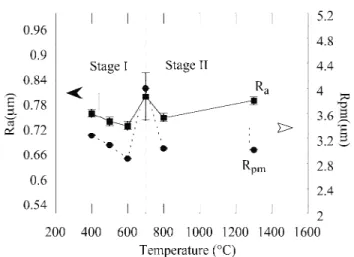
The roughness parameters for double-print films are shown as a function of first anneal temperature in Fig. 10. The average roughness, Ra, is nearly constant with a value of 0.74m for temperatures up to 600 °C but shows a sudden increase of approximately 0.1m between 600 and 700 °C. Above 700 °C, Ra seems to remain constant within the error of the measurements. Rpm, which is a measure of the height of the largest surface protrusions, also shows an anomalous change of 0.9m at 700 °C, but at higher and lower tempera-tures, this parameter does not vary greatly from an average value of 3.05m. Both Ra and Rpm show a minimum at a first anneal temperature of 600 °C, which also results in the optimum alumina surface coverage. The increase in Ra and Rpm at 700 °C corresponds closely with the transition between Stage I and Stage II densification regimens for the first Pt layer. The in-crease in Ra >700 °C can be attributed to the decrease in alumina surface coverage, which results in an in-crease in the size of the pores that pass directly through the Pt film.
The discussion above has centered on Pt films that were uniaxially pressed at 165 MPa after drying. Uni-axial pressing was used in an attempt to increase the green density of dried Pt films and in so doing improve the final sintered density. The primary difference ob-served between pressed and unpressed films was an im-provement of surface roughness. Figure 11 shows that there is a significant decrease in Raand Rpm, comparing pressed and unpressed films. This is true for both single-print and double-single-print films. It is believed that pressing flattens protrusions in the dried Pt layers as well as in-creases green density of the film as indicated by an ap-proximate 5% difference in thickness shrinkage between as-dried and pressed states as shown in Fig. 1. The im-proved densification of pressed layers is likely to result from a reduction of void volume and enhancement of interparticle contact, which can arise because of particle rearrangement and plastic deformation35of the platinum particles. The effect of uniaxial pressing on Raand Rpm is more pronounced for double-print films, which can be expected because single-print films exhibit incomplete coverage of the alumina surface due to coalescence and island formation of the Pt.
Although continuity of the Pt layer is important for use of the Pt film as a reaction barrier layer between PZT and alumina, it is also important that the Pt film exhibits good electrical conductivity to function as an electrode. The Pt film resistivity as a function of the first annealing tem-perature for double-print films is shown in Fig. 12. In general, it can be seen that the resistivities of the Pt films (13.5 × 10⁻⁶–18 × 10−6⍀ cm) are higher than the resistivity of bulk Pt (10.6 × 10⁻⁶⍀ cm).39 The higher measured resistivity of the films can be attributed to po-rosity and film surface roughness. One interesting obser-vation is that the best alumina surface coverage does not correspond with the lowest resistivity as one might FIG. 10. Dependence on roughness parameters Raand Rpmon the first annealing temperature of double-print Pt films. All films were sub-jected to a second heat treatment of 1300 °C for 18 min with a heating rate of 2 °C/min.
expect. Differences in grain size are not expected to be a cause for the differences in resistivity because analysis of micrographs indicates that all the films exhibit nearly the same average grain size of 3.2m (Table 2). The highest film resistivity is observed at 700 °C. Because this first anneal temperature also produces anomalies in both Ra and Rpm, it is likely that surface roughness contributes to the increased resistivity. Porosity within the thickness of the film is also expected to be a major contributor to the increase in resistivity because significant porosity within the film thickness was observed for films an-nealed at temperatures艋700 °C. By comparing alumina surface coverage, surface roughness, and resistivity, it is clear that the best Pt thick films obtained were bilayer films that were uniaxially pressed after drying each layer,
annealed at 600 °C in sintering Stage I for the first de-posited layer, and refired at 1300 °C at the peak of sin-tering Stage II for the second printed layer.
IV. CONCLUSION
This study of the processing conditions of Pt thick films onto alumina substrates bring has resulted in sev-eral observations that increase the understanding of these materials.
(i) Pt thick films exhibit three sintering stages: Stage I: T < 700 °C; Stage II: 700 °C < T < 1300 °C; Stage III: T > 1300 °C. By assuming that Pt sintering is controlled by lattice diffusion, the activation energy could be cal-culated for Stages I and II, and both were found to be different from the bulk Pt value. The difference in acti-vation energy could be due to the presence of carbon impurities, which influences the diffusion of Pt at low temperatures (<700 °C). The fact that the Pt film is con-strained by the underlying alumina substrate is also likely to be a factor in the activation energies observed for Pt film densification.
(ii) From the results obtained from the single- and double-print films, it has been hypothesized that there is a critical thickness that provides complete coverage of the substrate by the Pt film. The critical thickness should depend on the Pt grain size, interfacial energy between the Pt and alumina surface, and sintering temperature.
(iii) Double-print Pt layers with sequential heat treat-ment exhibit improved densification and surface cover-age of the underlying Pt. The first layer appears to act as a template for sintering of the second layer. The best alumina coverage is obtained with a 600 °C anneal of the first layer, which gives optimum neck formation in the first layer, followed by a 1300 °C anneal for the second layer.
(iv) For double-print Pt films, measurements of sur-face roughness and resistivity exhibit a maximum when the first layer is annealed at 700 °C; this temperature corresponds closely with the transition between Stage I and Stage II densification regimens.
(v) Uniaxial pressing of dried Pt films not only im-proves the densification of Pt layers by increasing the green density but also reduces surface roughness by flat-tening protrusions.
From these results it can be concluded that the best alumina coverage, surface roughness, volume density, and resistivity of screen-printed Pt films requires a com-bination of processing methods. Double-print films im-prove surface coverage, but each layer must be sintered in a proper densification stage to optimize the surface roughness. Finally, the optimized Pt films were success-fully used to produce PZT thick films with excellent electrical properties.
FIG. 11. Diagram showing the effect of uniaxial pressing on the roughness parameters Ra and Rpm for single-print Pt films (circle) sintered at 1200 °C for 18 min with a 2 °C/min heating rate and double-print films (triangle) with a first annealing temperature of 600 °C and second sintering temperature of 1300 °C with a hold time of 18 min and heating rate of 2 °C/min.
FIG. 12. Dependence of Pt film resistivity on first annealing tempera-ture of double-print Pt films sintered with a second firing temperatempera-ture of 1300 °C with a hold of 18 min and heating rate of 2 °C/min.
ACKNOWLEDGMENT
The authors acknowledge the CIME (Interdisciplinary Center of Electron Microscopy, EPFL, Materials Depart-ment, Lausanne, Switzerland) for providing the micro-scopes for our uses.
REFERENCES
1. Shen-Li Fu, J.K. Chung, and S.Y. Cheng, Jap. J. Appl. Phys.
24(24-2), 416 (1985).
2. H. Baudry, Hyb. Circ. 14, 71 (1987).
3. H.D. Chen, K.R. Udayakumar, L.E. Cross, et al., J. Appl. Phys.
77(7), 3349 (1995).
4. J. Collier, I.A. Cornejo, and M.J. Haun, Ferroelectrics 154, 47 (1994).
5. H.D. Chen, K.R. Udayakumar, L.E. Cross, et al., IEEE, 495 (1994).
6. H. Moilanen, S. Leppa¨vuori, and A. Uusima¨ki, Sen. Act. A 37–38, 106 (1993).
7. K. Uchino, Ceram. Bull. 65, 647 (1986).
8. W.S. Hackenberger, T.R. Shrout, and D.P. Pickrell, ISHM, 12, 53 (1996).
9. S.W. Smith and E.D. Light, IEEE Transactions on Ultrasonics, Ferroelectrics and Frequency Control 40, 727 (1993).
10. B. Morten, G. De Cicco, and M. Prudenziati, Sen. Act. A 41– 42, 33 (1994).
11. N. White and A. Cranny, Hyb. Circ. 12, 32 (1987). 12. G. Harsanyi and E. Hahn, Mechat. 3, 167 (1993).
13. B. Morten, G. De Cicco, A. Gandolfi, et al., Hyb. Circ. 28, 25 (1992).
14. M. Prudenziati, B. Morten, and G. De Cicco, Microel. Int. 38, 5 (1995).
15. S. Leppa¨vuori, A.H. Lozinski, and A. Uusimaki, Sen. Act. A
46 – 47, 391 (1995).
16. M. Monneraye, Act. Elec. 21, 263 (1978). 17. B.M. Austin, Sol. Sta. Technol. 12, 53 (1969). 18. L.C. Hoffman, Ceram. Bull. 63, 572 (1984).
19. J.R. Larry, R.M. Rosenberg, and R.O. Uhler, IEEE Transactions on Components, Hybrids and Manufacturing Technology 3, 211 (1980).
20. H. Baudry and F. Franconville, “Encres Se´rigraphiables pour Haute De´finition: Rhe´ologie et Impression,” Act. Elec. 21, 283 (1978).
21. R.W. Vest, Ceram. Bull. 65, 631 (1986).
22. J.G.E. Gardeniers, A. Smith, and C. Cobianu, J. Microm. Microe.
5, 153 (1995).
23. L.D. Madsen and L. Weaver, J. Elec. Mater. 21, 93 (1992). 24. Massimo Bersani, Bruno Morten, and Maria Prudenziati, J. Mater.
Res. 12, 501 (1997).
25. H-X. Zhang, S. Leppa¨vuori, A. Uusima¨ki, et al., Ferroelectrics,
154, 277 (1994).
26. J. Savage, in Handbook of Thick Films Technology, edited by P.J. Holmes and R.G. Loasby (Electrochemical Publications Lim-ited, Glasgow, 1976), p. 97.
27. T. Yamaguchi, S. Takeota, T. Iizuka, et al., Scr. Metal. Mater. 31, 1013 (1994).
28. G. De Cicco, B. Morten, and M. Prudenziati, Piezoelectric Thick-Film Sensors (Elsevier Science, New York, 1994).
29. M. McLean and E.D. Hondros, J. Mater. Sci. 6, 19 (1971). 30. K.T. Miller, F.F. Lange, and D.B. Marshall, J. Mater. Res. 5, 151
(1990).
31. P.J. Holmes and R.G. Loasby, Handbook of Thick Film Technol-ogy (Electromechanical Publication, Ayr, Scotland, 1976). 32. F.V. Lenel, Powder Metallurgy: Principles and Applications
(Metal Powder Industries Federation, Princeton, New Jersey, 1980).
33. R.W. Cahn, Materials Science and Technology: Processing of Metals and Alloys (Weinheim VCH, New York, 1991). 34. R.E. Hoffman and D. Turnbull, J. Appl. Phys. 22, 634 (1951). 35. W.D. Kingery, H.K. Bowen, and D.R. Uhlmann, Introduction to
Ceramics (Wiley Interscience, London, 1975).
36. D.A. Porter and K.E. Easterling, Phase Transformations in Metals and Alloys (Chapman & Hall, Boca Raton, 1981).
37. G.C. Kuczynski, Transactions of the AIME 85, 169 (1949). 38. K. Lu¨cke and K. Detert, Act. Metal. 5, 628 (1957).
39. D.R. Lide, CRC Handbook of Chemistry and Physics, 75th ed. (CRC Press, 1994–1995).