Dr. E. W. Fletcher Prof. A. L. Loeb Prof. C. C. Robinson J. M. Ballantyne R. Casale C. K. Crawford T. More, Jr. A. H. Nelson S. B. Russell F. W. Sarles, Jr.
A. MEASUREMENT AND CONTROL OF PROCESSES IN HIGH VACUUM
Recently, several researchers have observed poor results when using ring evapo-ration gauges to control evapoevapo-ration rates in high vacuum. The following discussion suggests why these results might be expected.
R
FILAMENT d
I+1 + II I+1 (I+ )
-20 VOLTS
+ 500 VOLTARIAC
- + 500 VOLTS
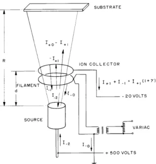
Fig. XVII-1. Electron and ion currents in a typical ring gauge.
Typical geometry for an evaporator equipped with a ring gauge is shown in Fig. XVII-1. In normal operation, electrons emitted from the filament impinge upon the source and cause it to evaporate by thermal heating. Some of the outgoing particles in the molecular beam are ionized by the incoming electrons. A fraction of these ions is collected on the ion collector and the resulting current is divided by the bombarding current. The number thus obtained is assumed to be proportional to the deposition rate. Unfortunately, this proportionality holds only at very low rates.
The deposition rate (1) is
*This work was supported in part by the U. S. Navy Bureau of Ships under Contract NObsr 77603.
D(A/sec) = 1. 505
x
10
5pA2
(2
(1500)1/2
where p is the evaporant vapor pressure just above the source, A is the atomic weight, p is the film density, a/R is the ratio of the source radius to substrate distance, and T is the source temperature. If we pick reasonable values, A = 100, p = 10 gm a _ 1
cm3 ' R 15' T
=
1500 *K, it is evident that a deposition rate of 100 A/sec requires a source pressure of approximately 1. 8 X 10⁻¹ mm Hg.For this geometry, the following relations also hold approximately for the currents flowing: ad I2 = (I 0+I 1) e 1+0 -0 +1-1 )(ead-1) I+1= K
1+0
I_1= yI+l whereI_0 is the electron current emitted from the filament;
I_1 is the electron current ejected from the ion collector by ion impact; I-2 is the total electron current bombarding the source;
I+0 is the total ion current formed by electron ionization; I+1 is the ion current intercepted by the collector;
a is the first Townsend coefficient; y is the second Townsend coefficient;
d is the source-to-ion-collector spacing; and
K is the collecting efficiency of the ion collector.
Solving these equations for I+1 yields the well-known Townsend breakdown equation.
K 1_0(e ad-1)
I+1
ad 1 - Ky(e -1)
The ratio a/p is a unique function of E/p for every material. Values for metals, appar-ently, have not been measured, except for mercury. With no alternative, we assume that the values for mercury are representative and, by picking d = 1 cm, obtain ad = a pd =
p 20pd = 3. 6, using the value of p corresponding to 100 A/sec and Brown's (2) data.
Because of the exponential dependence of the ion current on the beam pressure, the gauge is extremely nonlinear unless ad << . With the numbers chosen here, changing the deposition rate by a factor of 2 (from 100 A/sec to 200 A/sec) would change the ion
current by a factor of 40.
Experimentally, it is common practice to run these evaporators close to breakdown. The condition for breakdown is
ad
Ky(e -1) = 1Since y is usually of the order of 10-1, and K is approximately 3 X 10- 2 (based on solid-angle calculations), the exponent ad must be at least 3 or 4. This fact reinforces the assumptions made in the first analysis.
In addition to its nonlinearity, there are further objections to this type of evaporation gauge. It is not possible to analyze it without making severe approximations. It is not possible to calibrate it accurately, since the calibration changes as the source material becomes depleted; calibration changes also occur as K increases because of evaporant
build-up on the ion collector. Finally, since the output current is proportional to the widely varying electron bombardment current, electronic circuitry must be provided to separate the two.
C. K. Crawford
References
I. C. K. Crawford, The Use of Particle Optics in Thin Film Formation, S. M. Thesis, Department of Electrical Engineering, M. I. T. , June 1960.
2. S. C. Brown, Basic Data of Plasma Physics (The Technology Press of the Massachusetts Institute of Technology, Cambridge, Mass. , and John Wiley and Sons, Inc., New York, 1959), see Fig. 4. 39, p. 129.
B. FUNDAMENTAL PHYSICS OF THE THIN-FILM STATE
1. THE KERR MAGNETO-OPTIC EFFECTS IN FERROMAGNETIC FILMS a. The Polar Kerr Effect
When a ferromagnetic mirror is magnetized normal to its surface the light reflected from this surface undergoes the polar Kerr effect. The reflection equations for the polar effect are
R =r I +r I (1)
p pp p ps s
R = r I +r I (2)
s sp p ss s
Here, the incident electric field is I, the reflected electric field is R, the subscripts p and s refer to the components plane-polarized in the plane of incidence and perpendicu-lar to the plane of incidence, respectively, and the r's are the reflection coefficients
with the appropriate subscripts. Fresnel's equations express the ordinary metallic reflection coefficients r and r in terms of the usual optical parameters. The
Kerr-ss pp
effect coefficients rps and r were originally derived by Voigt (1) for metallic surfaces reflecting into vacuum or air. These coefficients are a function of the optical parameter and are proportional to Q, the complex magneto-optic amplitude which, in turn, is pro-portional to the magnetization of ferromagnetic material normal to its surface.
A dielectric coating on the surface of the ferromagnetic material will increase the magneto-optic effect. Therefore, the expression for r and r has been rederived for a dielectric-ferromagnetic interface.
-iQNoN cos 4
r = r = (3)
ps sp (No cos + N cos ')(N cos + No cos ')
We shall include the results for r and r for completeness.
ss pp N cos- N cos '
r
(4) N cos + Ncos ' Ncos - N cos ' r (5) PP Ncos + N0 cos 'In Eqs. 3, 4, and 5 N is the complex index of refraction of the ferromagnetic material, N is the index of refraction of the dielectric, is the angle of incidence in the
dielec-o
tric, and
4'
is the angle of refraction in the ferromagnetic.Equations 1 and 2 have the same form for both the longitudinal and the polar Kerr effects and only the expressions for r and r are different. Therefore, a ferromag-netic surface coated with a thin dielectric film and magnetized in the normal direction can be treated by using the results derived by Sarles (2). It is only necessary to change the Kerr reflection coefficients appropriately.
b. The Transverse Kerr Magneto-optic Effect
If the magnetization of a ferromagnetic surface is transverse to the plane of incidence and parallel to the surface, the condition for the transverse magneto-optic effect exists. Only the light plane polarized in the p-plane is affected by the magnetization. There is a small change in the amplitude and the phase of this reflection coefficient when the magnetization M is reversed. Therefore, the reflection equations are of the form
R =r
I
(6)
s ss s
R =r I +r I (7)
The reflection coefficients r and r are the same as those of Eqs. 4 and 5. The
ss pp
coefficient r is the small change in the p-plane reflection which depends upon the magnetization. For a dielectric-ferromagnetic interface, r is given by
2
i2QN sin
P
cos Cr o (8)
k (Ncos + N cos 4')
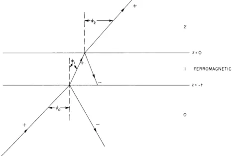
The transmission of light through a thin film magnetized in the transverse direction is of interest because the existence of a transmitted wave will alter the reflection prop-erties. Figure XVII-2 shows a light incident from a dielectric 0 on a ferromagnetic film 1. Behind the film there is a second dielectric 2 into which the rays finally pass. In this discussion only the radiation with the electric vector in the p-plane will be
+
2
z=0O
I FERROMAGNETIC
z- -t
Fig. XVII-2. Rays transmitted through a thin ferromagnetic film.
V= Ey 0 o jo0 c s o0 Zoo0 oCOS 4o y= je cos 01 Zo=, 12 COS 02 I=Hz O 0 0
LINE 0 LINE I LINE 2
considered, as this is the only component affected by the magnetic field.
At each interface, the tangential components of E and H are continuous, and it is therefore simpler to discuss this problem strictly in terms of these tangential compo-nents. It is well known that the propagation of the tangential fields in a dielectric or metal is analogous to a transmission-line problem (3). Figure XVII-2 now reduces to the form shown in Fig. XVII-3. Line 1, which represents the ferromagnetic, is not a true transmission line but obeys Eqs. 9 and 10 that are similar to those of a lossy transmission line: -ylx +Yl E = E+ e + El e (9)
ly
ly+
ly-H = 1 E ly+ e -E ly - e +J (10) where N 1 cos 1 1 N1 1p = arc tan (Q tan 1)
The x-components of the E field in the ferromagnetic are given by
-(sin 1 - iQ cos 1 ) Elx+ = Ely+ (11) (cos 4 1 + iQ sin ) 1 y
-(sin 41
+iQ cos 4
)
1 Elx- = Ely- (1Z) (cos 1 - iQ sin 1)With this information, it is a straightforward problem to find the reflection and the transmission associated with a thin ferromagnetic film magnetized in the transverse direction. For example, if we consider film 1 to be infinitely thick, then only the Ely+ wave exists in the ferromagnetic film. Under this condition, the ferromagnetic film becomes an impedance rle+p at the end of the transmission line analog for the dielec-tric 0. The complex phase angle p changes sign when the magnetic field is reversed, and this termination illustrates how the magnetization alters the wave impedance of the ferromagnetic film. From transmission-line theory, the reflection and transmission of the tangential field are given by
Eyo- l ejp
--
(13)
Eyo+ 1 ep - o and Eyl+ 2 11 ej p - (14) Eyo+ ?1 ejp + 0If the ferromagnetic film is thin enough so that an appreciable negative traveling wave appears, then the problem is a little more complex. Fortunately, the character of the radiation within the film is almost that of a lossy transmission line, and only
corrective terms need to be introduced because of the magneto-optic effect. The dielec-tric film 2 will present some impedance Z(O) at z = 0. The reflection coefficient in the ferromagnetic can be expressed as
Z(O) - 1 2jpZ(O)
r +
AFr=
- (15)Z(0)
+ l
(Z(0)+ I)
where r is the ordinary lossy line reflection coefficient, and AF is the additional com-ponent arising from the magneto-optic effect.
The impedance z = -t at the other surface of the film is, then, 1(Ie - 2y t) jp(l+e-2yt 2 2e - yt
Z(-t) + AZ(-t) = + -+ (1 6)
(1- re-Zyt T1 (lre-2yt 2 (lre-2t) 2
Here, Z(-t) is the impedance that would be read from a Smith chart for a lossy line. This impedance has the form
-2y ll (1 + e-2 t ) Z(-t) = (17) (1_ ie-2yt
The Kerr-effect component of the impedance at the surface is, then, jp(Z(-t)) 201
AFeZYt
AZ(-t) = + (18)
1 (1-e-yt )
Because the ferromagnetic film presents the impedance Z(-t) + AZ(-t) to line 0, the reflection coefficient at the 0, 1 interface is given by
z(-t) + AZ(-t)
-T
0
F(-t)
=(19)
Z(-t) + AZ(-t) + n
°References
1. W. Voigt, Magneto- und Elektrooptik (Verlag B. G. Teubner, Leipzig, 1908). 2. F. W. Sarles, High Speed Computer System Research, Quarterly Progress Report No. 11, Computer Components and Systems Group, M. I. T. , 31 July 1960, pp. 9-11.
3. R. B. Adler, L. J. Chu, and R. M. Fano, Electromagnetic Energy Transmis-sion and Radiation (John Wiley and Sons, Inc., New York, 1960).
2. INVESTIGATION OF THE KERR MAGNETO-OPTIC EFFECT ON VARIOUS MATERIALS
Research among published works has been carried out for the purpose of finding mate-rials that give larger Kerr rotations than do the commonly used films of iron, nickel, cobalt, and permalloy. Measurements (1, 2) of the Kerr rotations have been made on a large number of ferromagnetic materials, including the metals Fe, Ni, Co, their oxides and alloys, and alloys of Mn. None of these materials give substantially larger rotations than do the metals Fe and Co. Pure iron and cobalt give Kerr rotations of approximately 20 minutes, while a rotation of 27. 64 minutes, the largest rotation recorded, has been observed on ferrocobalt.
Recent investigators have studied the magnetic behavior (3, 4, 5) and domain struc-ture (6, 7, 8) of Bi-Mn and have used the Kerr magneto-optic effect (6, 8), as well as the
Faraday effect (6), to observe magnetic domain patterns in this material. Photographs obtained by Roberts (6), using the Faraday and the Kerr effects, are of equal contrast for domains in Bi-Mn films. Roberts (6) reported Faraday rotations of 50 for his samples. He did not report the magnitudes of the Kerr rotations, but the high contrast of his pic-tures seems to indicate a very large rotation. As we have stated, the Kerr effect on alloys of Mn, including an alloy of Mn and Bi, has been measured (1, 2). A rotation of only 1. 32 minutes was then reported. In the light of recent investigations of Bi-Mn, it must be concluded that Barker's (1) measurement was either conducted on a magnetically unsaturated sample, or the alloy had not formed the compound Bi-Mn.
A procedure for making thin films consisting principally of Bi-Mn has been reported (8). An experimental investigation of the Kerr magneto-optic effect in films of Bi-Mn is being considered by our group.
J. M. Ballantyne References
I. S. G. Barker, Proc. Phys. Soc. (London) 29, 1 (1916).
2. R. de Mallemann and F. Suhner, Pourvoir rotatoire magnetique (effet Faraday) et Effet magn6to-optique de Kerr, Tables de Constantes et Donnees Numeriques, No. 3 (Hermann et Cie., Paris, 1951).
3. 4. 5. 6. 7. 8. Phys. B. E. R. B. J. H. 28,
W. Roberts, Phys. Rev. 104, 607 (1956). Adams, J. Appl. Phys. 23, 1207 (1952). R. Heikes, Phys. Rev. 99, 446 (1955).
W. Roberts, Phys. Rev. 96, 1494 (1954). B. Goodenough, Phys. Rev. 102, 356 (1956).
J. Williams, R. C. Sherwood, F. G. Foster, and E. M. Kelley, J. Appl. 1181 (1957).
3. OPTICAL STUDY OF SWITCHING AND MAGNETIC THIN FILMS
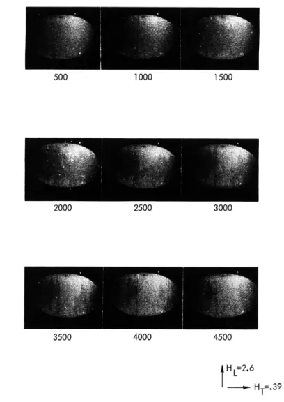
A number of photographic series have been taken showing dynamic flux reversal of thin magnetic films. One of these series is shown in Fig. XVII-4. In this figure, the
500 1000 1500
2000 2500 3000
3500 4000 4500
H L=2.6
- HT=.39
reversal time is approximately 5
psec.
The magnitude of the reversal field HL is 2. 6 oe; a static transverse field HT of 0. 39 oe is also applied to the film. The reversal occurs almost entirely from domain wall propagation; nucleation of domains occurs primarily at the edges of the specimen. (Time intervals after application of the reversal field are indicated in nanoseconds under each photograph.) At higher reversal fields, it is difficult to determine the magnetic configuration from a photographic series. Equip-ment problems and changes in the reversal mode are responsible for this difficulty.In the reversal mode at higher fields, large domains are no longer apparent, and lack of resolution at this time prevents determination of any type of fine structure in the magnetic configuration. It is believed, however, that this second mode is a combination of rotational reversal in various regions and domain wall propagation that originates from nucleation sites created by localized rotation in regions of low magnetic anisotropy.
F. W. Sarles, Jr.
4. MEASUREMENT OF THE KERR EFFECT IN NICKEL-IRON FILMS
The lead sulfide cell which replaced the photomultiplier described in previous prog-ress reports has been installed in order to extend the Kerr effect measurements into the infrared region. A high-gain, selective amplifier with a twin-Tee filter tuned to 200 cps has been constructed for use with the sulfide cell because the sensitivity of the cell is lower than that of the photomultiplier. A synchronous detector has also been constructed and is used after the amplifier to detect only the desired frequency com-ponent from the output of the sulfide cell.
At present, the sulfide cell-amplifier detector system is working, but stray mag-netic and electrostatic pickup at the sulfide cell and its associated wiring contribute a background level that almost obscures the optical response of the cell. More effective shielding is being installed to reduce this background level.
S. B. Russell
C. CRYSTAL ALGEBRA
1. THE CALCIUM SILICIDE STRUCTURE
The calcium silicide (CaSi2) structure is a very interesting one from the point of view of the crystal algebra. Two sources of information regarding this structure are available, namely an article by Boehm and Hassel (1), and a description, based on this article, by Wells (2). A drawing made by Wells is so little enlightening that an algebraic analysis seemed to be called for.
Boehm and Hassel state that in CaSi2 each Ca is surrounded by seven Si-s: three in
the opposite side of the Ca (these six form an antiprism with Ca at the center), and a seventh at approximately 3 A from the Ca along a straight line perpendicular to the planes containing the Si triangles. Wells describes this same structure as consisting of alter-nate Ca and Si layers, a silicon layer being made up of "a puckered graphite layer or a
section of the diamond structure parallel to the octahedron plane (111), in which each Si has three neighbours at 2. 48 A, the bond angles having the normal tetrahedral value. The Ca atoms lie between these layers with six Si neighbours (Ca-Si 2. 99 A)."
Our first task is to investigate the consistency of these two descriptions; the second, to determine whether these descriptions are sufficient for a unique determination of the
structure. We shall show that the answer to the first question is affirmative, that to the second negative.
In terms of the crystal algebra described in three articles by Loeb and Morris (3), the calcium silicide structure contains close-packed planes of Ca and of Si that are stacked in a manner not encountered previously. There are twice as many Si-planes as there are Ca-planes; the distance between adjacent Si-planes is approximately 1 A,
while that between a Ca-plane and an adjacent Si-plane is approximately 2 A. Each Ca is surrounded octahedrally by six Si-s. The seventh Si gives us an important clue to the way in which the planes are stacked because it connects the Ca to a plane that is not immediately adjacent. This description is consistent with both sources (1, 2); the dis-tances between adjacent planes given by Boehm and Hassel, and in this report, agree
with those between ions given by Wells.
To describe the way in which the close-packed planes are stacked, recall that each plane can occupy one of three positions, described by D, E, and F (see Morris and
Loeb (3, 4)). The stacking of close-packed planes in CaSi2 is subject to the following
constraints:
1. Two adjacent Si-planes are 1 A apart.
2. Each Ca-plane is removed 2A from its nearest Si-plane.
3. Adjacent planes never have the same one of the three stacking symbols D, E, and F.
4. Two Si-planes on opposite sides of a Ca-plane never have the same one of the three stacking symbols D, E, and F (antiprism constraint).
5. Of the two Si-planes that are next-nearest neighbors to a Ca-plane, one and only one has the same stacking symbol as does the Ca-plane (seventh-Si constraint).
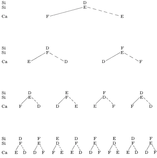
Starting with a pair of adjacent Si-planes, one in the D position and the other in the E position, we have two choices for the third plane, which contains Ca-s. If this plane is placed in the D position, then the seventh neighboring Si lies directly below each Ca; the next two Si-planes, in that case, must be successively in the F and E positions, in
order to give Ca its desired seven Si-neighbors. If the Ca-plane is placed in the F position, then the seventh Si must lie directly above the Ca, so that the next two
Si-planes are necessarily in D and F positions. Thus the choice of position of each Ca-plane uniquely determines the position of the next pair of Si-Ca-planes, but each time the Ca-plane may be in one of two positions, the position depending on whether the seventh Si lies directly above or below the Ca. We can denote the multiple choices by the tree shown in Fig. XVII-5, in which a solid line indicates a choice of Ca-plane position which is such that the seventh Si lies above the Ca; a broken line, that the seventh lies below the Ca. Observe that this tree does not continue to branch indefinitely, but that the same pattern repeats itself. As a matter of fact, there are six possible patterns in the decision tree, as given in Fig. XVII-6.
The tree of Fig. XVII-5 can be rewritten in terms of the six blocks of Fig. XVII-6, as shown in Fig. XVII-7. In the third figure are shown all of the stacking patterns that are possible, subject to the constraints enumerated above. The solid and dotted arrows have the same significance here as in Fig. XVII-1.
D F E
Ca
D E FF
D
E
Si D Si E\ Ca F E SF\ D D F DE EE
E
D
E\
F
F
Si D F Si F E Ca E D D F E D FE D FED
F E E D D F FED
F
F
E
ED
D
F
Fig. XVII-6.
Possible patterns in decision tree for CaSi
2.
6
3
Fig. XVII-7.
Decision tree rewritten as a flow diagram.
We conclude that the descriptions given by Boehm and Hassel and by Wells are
not sufficient for a unique and unambiguous description of the CaSi
2crystal
struc-ture. It follows from Fig. XVII-7 that it might be a structure in which each
seventh Si lies either above or below the Ca; in that case, we would follow
the 1:_Z2 pattern (or 3:_4 or 2-33, which are equivalent), with the resulting
stacking pattern:
Si D Si E Ca F Si D Si F Si E
The periodicity of this structure in the h-direction would be two sets of CaSi2 layers.
On the other hand, there might be alternate Ca layers with seventh Si above, and Ca layers with seventh Si below. In this case, in Fig. XVII-7 we should follow a path con-taining alternately solid and dotted arrows; in other words, go straight around the circle.
Then, the pattern is
Si D Si E Si E Si D Ca F Ca E Si D Si F Si F A Si D Ca D Ca E Si E Si F Si F Si E
Ca
D
Ca
F
The periodicity of this letter structure would be six sets of CaSi2 layers. There are
many more ways of traveling around the circle of Fig. XVII-3; when further X-ray anal-ysis of this structure is performed, possibly, the periodicity of the structure will give a clue to the stacking.
A. L. Loeb
References
1. J. Boehm and O. Hassel, J. Inorg. Chem. 160, 152 (1927).
2. A. F. Wells, Structural Inorganic Chemistry (Oxford University Press, London, 2d edition, 1950), p. 558.
3. A. L. Loeb, Acta Cryst. 11, 469 (1958); A. L. Loeb and I. L. Morris, Acta Cryst. 13, 434 (1960); A. L. Loeb, A modular algebra for the description of crystal
structures (submitted for publication to Acta Cryst.).
4. A. L. Loeb and I. L. Morris, High Speed Computer System Research, Quarterly Progress Report No. 3, Computer Components and Systems Group, M. I. T., 31 July 1958,