HAL Id: hal-03090167
https://hal.univ-lorraine.fr/hal-03090167
Submitted on 29 Dec 2020HAL is a multi-disciplinary open access archive for the deposit and dissemination of sci-entific research documents, whether they are pub-lished or not. The documents may come from teaching and research institutions in France or abroad, or from public or private research centers.
L’archive ouverte pluridisciplinaire HAL, est destinée au dépôt et à la diffusion de documents scientifiques de niveau recherche, publiés ou non, émanant des établissements d’enseignement et de recherche français ou étrangers, des laboratoires publics ou privés.
Distributed under a Creative Commons Attribution - NonCommercial - NoDerivatives| 4.0
Sequential run of the PEO process with various pulsed
bipolar current waveforms
Vitalios Ntomprougkidis, Julien Martin, Alexandre Nominé, G. Henrion
To cite this version:
Vitalios Ntomprougkidis, Julien Martin, Alexandre Nominé, G. Henrion. Sequential run of the PEO process with various pulsed bipolar current waveforms. Surface and Coatings Technology, Elsevier, 2019, 374, pp.713-724. �10.1016/j.surfcoat.2019.06.057�. �hal-03090167�
Sequential run of the PEO process with various pulsed bipolar current
waveforms
V. Ntomprougkidis1,2, J. Martin1,2,*, A. Nominé1,3, G. Henrion1,2
1 Institut Jean Lamour – UMR 7198 CNRS – Université de Lorraine – 2 allée André Guinier,
F-54011 Nancy, France
2 Laboratoire d’Excellence Design of Alloy Metals for low-mAss Structures (‘LabEx
DAMAS’) - CNRS - Université de Lorraine – 7 rue Félix Savart, F-57070 Metz, France
3 Department of Nanophotonics and Metamaterials, ITMO University, St. Petersburg 197101,
Russia
Highlights
Behaviour of micro-discharges explained by a mechanism of charge accumulation. Coating growth rate and quality enhancement by sequential processing.
Appearance of the beneficial soft regime is affected by sequential processing. PEO sequenced treatments open opportunities for energy reduction.
Abstract:
Oxide coatings were produced on a 2024 aluminium alloy using a pulsed bipolar current plasma
electrolytic oxidation (PEO) process in an alkaline electrolyte. The use of sequences including
various current waveforms during the same treatment was investigated, mainly by applying
various combinations of two different anodic to cathodic charge quantity ratio (RCQ = 0.9 and
6.0). The morphology of the produced PEO coatings was observed using scanning electron
microscopy while the behaviour of the micro-discharges was characterized in real time with
the process using plasma diagnostic techniques. Compared with conventional treatments
conducted in a single sequence, results evidenced that the thickness and the compactness of the
PEO coating are enhanced by switching from a high to a low RCQ value in the course of the
process. In contrast, reverse sequenced treatments leads to a significant deterioration of the
produced PEO coating. A possible explanation exposed in the present study consists in
considering the main role played by the mechanism of charge accumulation at the electrolyte /
oxide interface on the micro-discharges behaviour with respect to the coating morphology and
the applied charge quantity ratio. Finally, by establishing a relationship between process,
physical and material quantities, this study demonstrate that the use of sequenced treatments
open opportunities for a better energetic management of the PEO process.
Keywords: Plasma Electrolytic Oxidation (PEO); Micro-Arcs Oxidation (MAO); Pulsed
1. Introduction
Plasma electrolytic oxidation (PEO) is a surface engineering process suitable for
lightweight metals (Al, Mg, Ti) and their alloys to form protective ceramic coatings [1].
Based on an electrochemical conversion of the metal surface, the rapid growth of the oxide
layer takes place at high potential beyond the critical dielectric breakdown threshold of the
growing insulating layer. This leads to the development of numerous tiny and short-lived
micro-discharges (MDs) that move randomly over the processed surface [2-4]. When applied
to aluminium alloys, the resulting PEO coatings exhibit improved hardness (1500 Hv)
and wear resistance (1.10-4 mm3/N.m). Indeed the index of crystallinity of the formed aluminium oxide remains close to 100% (amorphous in the case of conventional acid
anodizing) including the presence of γ-Al2O3 and the −αAl2O3 in various proportion [5,
6]. Moreover, as it uses diluted alkaline electrolytes free of any heavy metals or
carcinogenic, mutagenic and reprotoxic (CMR) substances, the PEO process complies with
the present environmental and health regulations. Therefore, it gains a growing interest in
various domains (transport, energy, medicine, leisure and home) to replace conventional
chromic or sulphuric acid anodizing processes. Despite these advantages, its deployment at
the industrial scale remains still restricted due to relatively high costs arising from the use
of high current densities (up to 10 - 100 A/dm2) and high voltages (up to 400 – 1000
V) that renders the process highly energy consuming. In the literature, works devoted to
improve the energy efficiency of the PEO process are abundant but two main approaches
emerged.
Firstly, by adopting a process engineering approach, the main way that is explored consists in
adjusting the PEO processing parameters, mainly the electrolyte composition [7-11] and the
applied electrical signal [3, 4, 12-17]. On this last point, the electrical parameters play an
important role in the process since they have a strong influence on both the space and time
has been established that the use of a pulsed bipolar current (PBC) to supply the electrodes
results in a better quality of the coatings in terms of thickness and compactness [12,18]. Under
this PBC mode, additional works have also found that the suitable adjustment of the waveforms
of the current pulse, i.e. the anodic and cathodic current amplitudes, the pulse duration and the
current frequency can determine the growth mode of the oxide films. Particularly, pioneer
works from Jaspard-Mécuson et al. have shown that the right control of the charge quantity
ratio RCQ = Qp / Qn (ratio of positive Qp to negative Qn charge quantities applied during one
period of the current pulse) is crucial and promotes the appearance of a particular growth regime called “soft” regime [3]. The appearance of this “soft” regime is mainly conditioned by maintaining a RCQ that must be set less than one, more specifically in the range between 0.8
and 1[3,4,19]. This regime that occurs after a certain initial period of conventional PEO arcs
regime is always associated with both a gradual decrease in the electrical voltage, a change in
the optical emission due to the gradual disappearance of the MDs and a reduction in the acoustic
noise [3]. It is also worth noting that despite the gradual disappearance of visible MDs during “soft” regime, advantages of PEO process are kept and some of them are emphasized (e.g. higher growth rate, higher proportion of high temperature crystalline phases, less large
porosities). In addition, it was also established that the occurrence of this beneficial “soft”
regime could happen earlier in the process by working with both a higher frequency and / or a
higher current density leading therefore to a significant reduction in the specific electrical
energy consumption (i.e. the electrical energy needed to grow 1 µm thick of compact oxide
layer over 1 m2 processed surface) [4].
The second approach, regarding the improvement of the energy efficiency of the PEO
process, consists in getting a better understanding of the physicochemical mechanisms that
govern the growth of the PEO oxide layers under an electrical discharge regime. Although
of what happens during the PEO process, growth mechanisms are still not well understood;
clear relationship between the process parameters, the micro-discharge properties and the
coating growth remains to be established as well. However, it is usually admitted that such
growth mechanisms can be classified into two groups, those that describe the oxidations
processes of the metal when submitted to an electrical discharge regime [20-25], and those that
describe the dielectric breakdown processes of the insulating coating when surrounded with a
cooled and a conductive liquid [26-32]. In the first group, on the basis of the steam and gas vial
model, Klapkiv et al. [20, 21] suggested a single-discharge model with a core/shell structure.
Later, Sundararajan et al. [22, 23] showed that the molten material, which is ejected through
discharge channels, is oxidized, rapidly solidified and deposited on the surface, promoting thus
the growth of the oxide layer. For Yerokhin et al. [24], two simultaneous mechanisms of the
metal oxidation take place through the discharge channels including a plasma-assisted
oxidation and an electrochemical-assisted oxidation. More recently, by using 18O isotope tracers through PEO coatings, Matykina et al. [25] concluded that migration of oxygen is the
result of two concomitant mechanisms, i.e.one by the solid-state diffusion of oxygen and
another due to water molecules trapped in cavities which within the plasma decompose and
form ions and radicals.For the second group of mechanisms, i.e. those that tend to explain the
occurrence of the MDs at the metal surface during the PEO process, Hussein et al. [26-27]
suggested a multi-discharge model including three types of discharges igniting at several
locations and at different times through the coating thickness: A-type discharges that appear
on the fine impurities located on the top surface of the coating, B-type discharges that cross the
overall thickness of the coating, and C-type discharges that occur in the micro-sized porosities
of the coatings. On the basis of optical emission spectroscopy measurements, Jovović et al. [28] were able to confirm these three types of discharges. Using a silicate-based electrolyte,
anions adsorbed on the topmost surface of the growing oxide layer. Later, Cheng et al. [30-32]
enriched Hussein’s model by including D- and E-type discharges in order to explain the typical
morphology of the PEO coatings, i.e. the presence of an outer porous sublayer filled with
electrolyte and an inner dense sublayer. More recently, mechanisms involved in PEO
treatments conducted under the specific “soft” sparking mode have been the subject of deeper
investigations with a particular focus on the influence of the cathodic half-period in the ignition
of MDs and coating growth [19, 33-35]. Indeed, if all studies agree with the fact the cathodic
polarization is needed to prevent large and detrimental MDs, few works explain why this
happens. Martin et al. evidenced that the appearance of the MDs is delayed with respect to the
applied anodic current pulse, this delay being strongly influenced by the current waveform
applied [19]. Considering the capacitive behaviour of the electrolyte / oxide system, authors
assumed a phenomenological mechanism of anionic charge accumulation that takes place
during the anodic alternation through the electrical double layer (EDL) located at the electrolyte
/ oxide interface until breakdown occurs. They also demonstrate that the magnitude of the
cathodic current alternation influences mainly the dynamics of formation of the EDL (separated
cationic H+ and anionic OH- species) during the subsequent anodic current alternation. Indeed, a significant excess in the cathodic current (ratio of charge quantity RCQ << 1) is associated to
an excessive dispersion of anionic charges at the oxide / electrolyte interface and thus results
in a longer anionic charge recharging process to restore the EDL during the subsequent anodic
current. More recently, Nominé et al. considered the EDL thickness using Debye-Hückel's
relation and the ion mobility in an alkaline silicate electrolyte (mainly K+, Na+, H+ and OH-). By varying the current pulse frequency, they estimated that anodic EDL requires ~200 µs to
form. Considering a bipolar current pulse with 50% duty cycle, this corresponds to a frequency
of ~2.5 kHz. [33]. At the same time, Rogov et al. suggested that the cathodic polarization is
of the oxide – electrolyte interface that in turn reinforces the potential drop and the electric
field at the metal / oxide interface during the subsequent anodic polarization. Based on this
consideration, authors explained why, within “soft” regime conditions, it is possible to enhance
anodic oxidation of the metal substrate and high-energy processes without strong discharges
[34, 35].
The present study aims at contributing to a better understanding of the physical mechanisms
that allow the coating growth under discharge regime while keeping in mind the necessity to
decrease the energy consumption of the PEO process, as well as improving the produced
coating quality. For this purpose, the main idea consists in investigating the PEO process by
using sequential treatments with various set of electrical parameters, mainly by applying
various RCQ to the electrodes. Particularly, two very different RCQ were considered in this
work because they are known to result in opposite effects in terms of the produced PEO coating
morphology and the electrical energy consumption. The first RCQ considered, RCQ = 6.0,
allows to rapidly build up a thick but highly porous oxide layer – large open cavities - while
the second RCQ, RCQ = 0.9, provides a thinner but a more compact coating with a substantial
reduction in the energy consumption due to appearance of the “soft” regime in the course of
the process [3, 4, 16]. By taking advantage of these two opposite electrical conditions within
the same sequenced PEO treatments, it may be expected to achieve a synergetic effect which
could results in the elaboration of improved PEO coatings performance with a significant
energy gain. The effects of a sudden modification of the electrical conditions in the course of
a PEO process is closely investigated and discussed by taking into account the correlation
between several criteria based on the process monitoring data (voltage- and current-time
responses), the MDs behaviour (light emission, surface density, spatial distribution and size)
with results collected from reference treatments run within a single sequence are also
considered for discussion.
2. Material and experimental procedure
Sample made of Al2024 aluminium alloy (3.8 - 4.9 at. % Cu, 1.2 – 1.8 at. % Mg, 0.3 – 0.9
at. % Mn and Al as balance) were PEO processed in a solution of potassium hydroxide ([KOH]
= 1 g.L-1 0.018 mol.L-1) and anhydrous sodium silicate ([Na2SiO3] = 1.65 g.L-1 0.014 mol.L -1) diluted in deionized water. The electrical conductivity and pH values are 2.8 mS.cm-1 and
12.5, respectively. The composition of the electrolyte remained unchanged for all the
treatments, its influence on the PEO process was not the subject of the present study. A cooling
device allows keeping the electrolyte temperature at about 30 °C. Two rectangular titanium
counter-electrodes (200 200 1 mm3 in size) face both sides of the processed aluminium sample (50 30 6 mm3 in size). The electrode gap between each titanium counter-electrode and the working aluminium sample is fixed at 90 mm.
PEO treatments were conducted by applying bipolar current to the electrodes. The use of a
current controlled power supply makes it possible to optimally set and control the anodic and
the cathodic currents amplitude, and therefore to control the respective charge quantities
delivered to the electrolyser system. Various sequential PEO treatments were performed by
changing the value of the charge quantity ratio (RCQ) during the process. It is worth noting
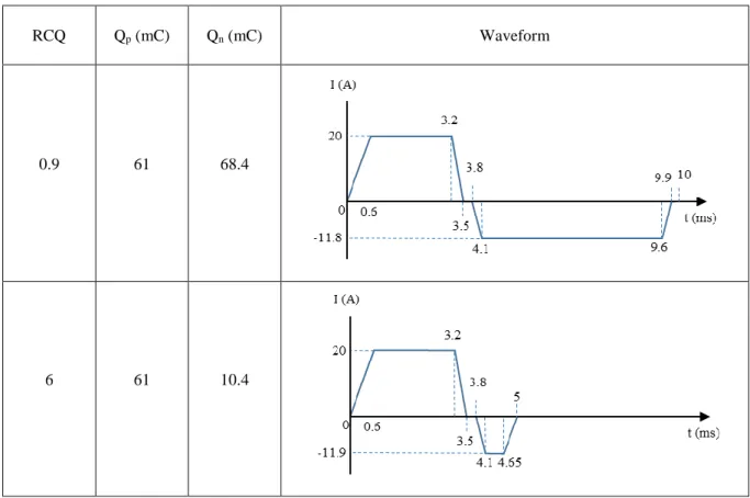
that the two RCQ values considered in this study were set by adjusting only the waveform of
the cathodic current pulse, while maintaining the anodic one unchanged. Values of current
pulse magnitude, duration, frequency, and charge quantity are given in Table 1 together with a
treatments investigated, the samples were systematically processed for 20 min with a first RCQ
value. At 20 min processing, the current supply was switched to the second RCQ value without
stopping the PEO treatment. Process continued with this second RCQ value for 30 min.
Consequently, the total duration of all the sequential PEO treatments investigated was equal to
50 min. In parallel, and for comparison reasons, four reference treatments were also conducted
that consist of single PEO treatment runs with the same RCQ values for 20 and 50 min (See
Table 2).
Voltage and current waveforms were recorded at periodic intervals during the process using
a 1 GHz bandwidth oscilloscope (Agilent 54832B). The light emitted by the micro-discharges
(MDs) was detected with a photomultiplier (Hamamatsu R928), over the full range of visible
spectrum. The recorded signal hence corresponds to a wavelength-integrated value. The output
signal was amplified by a 300 MHz bandwidth current amplifier (Stanford Research Systems
SR445) and recorded together with the current and voltage signals. As a complement, by using
a high speed camera (Photron SA1.1), video recordings of the MDs were precisely conducted
at time when the transition from the first RCQ to the second one occurs. Only the lower part of
the sample is filmed over an area of 5.4 cm2 (30 18 mm2) providing a spatial resolution of 0.015 mm2/pixel,which is at least three times lower than the average area of MDs that were detected in the experiments. The acquisition rate was fixed at 150 000 frames per second that
corresponds to a time resolution of 6.6 µs. Image processing was performed using the
home-developed TRACE software [36, 37]. It makes it possible to discriminate MDs from noise and
to characterize their behaviour in the course of the treatment (spatial distribution, density and
size).
X-ray diffraction (XRD) measurements were performed for the phase identification of the
produced oxide coatings. A Bruker D8 ADVANCE diffractometer (Cu-Kα , λ=1,5406 Å) was
°. The grown layers were observed by scanning electron microscopy (FEG-SEM Philips
XL30). Prior to their observation, the samples were cut, mounted in resin and polished
successively with various grades of SiC abrasive papers. A final step polishing was performed
with a 1μm diamond paste. Observation of the coating cross-section was performed in
back-scattered electron mode (25 kV accelerating voltage) while observation of the coating
top-surface was conducted in secondary electron mode (5 kV accelerating voltage). Estimations of
the thickness and the void fraction of the coating were conducted on cross-section SEM
micrographs by using image processing that discriminates the coating from the substrate and
the surrounding molding resin. The thickness and the fraction of voids were determined as the
average values of 10 measures taken on cross-section over 10 different positions (each 500
µm). Moreover, it is necessary to clarify that voids correspond to cavities throughout the
coatings that are larger than 1 µm in diameter, finer porosities being not detected after image
processing. Finally, the chemical composition and the distribution of elements in the
synthesized oxide layers were determined by EDX analyses on sample cross-sections.
3. Results
3.1 Establishment of the “soft” regime
Fig. 1 shows the time evolution of the anodic voltage amplitude for the different sequenced
treatments investigated as well as for the associated reference treatments consisting of a single
sequence.
At the beginning of the process, all curves reveal a quite similar trend with a strong increase
in the voltage amplitude. During this early stage that only lasts for a few seconds, an initial
amorphous oxide thin film grows with no visible micro-discharges (MDs) while a bluish
at which the slope of the voltage curves significantly reduces (at about 620 V) is commonly
designated as the dielectric breakdown voltage of the formed oxide layer. Once this specific
voltage value is reached, the ignition of small blue-white MDs starts over the processed surface
[7, 15, 30]. Until the switching point that will occur at 20 min, Fig. 1 shows that the anodic
voltage amplitude follows a much reduced increase rate and the visible MDs become fewer
and larger and they gradually turn into orange-red colour. It can also be noticed that during this
stage, the anodic voltage amplitude reveals slight differences depending on the electrical
conditions applied. Right before 20 min, the anodic voltage reaches 726 5 V for the treatment
performed with the low RCQ (RCQ = 0.9) while it reaches 755 5 V for the treatment
performed with the high RCQ (RCQ = 6.0).
Right after 20 min, a significant voltage drop is observed for the treatment that switches
from the high RCQ to the low one while a slight voltage jump is noted for the reverse sequence.
Particularly for the first, the anodic voltage decreases suddenly from 755 5 V to 540 10 V
over less than 5 s following the transition, then increases for a period of 3 min and finally
decreases with a much lower rate to stabilize at about 558 10 V until the end of the treatment.
For this specific sequence treatment, it is also worth noting that from the switching time at 20
min to the end of the process at 50 min, the anodic voltage amplitude constantly remains lower
than all the other PEO treatments investigated. Additionally, Fig. 1 shows that the time at which
the anodic voltage gradually decreases – usually referred to as the time of the “soft”-regime
appearance and noted tSR in Table 1- occurs earlier for this specific sequenced treatment (tSR =
23 1 min) than for the single reference treatment conducted with the low RCQ only (tSR = 30 1 min).
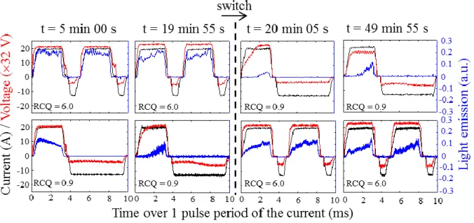
Chronograms in Fig. 2 show the variations of the light emission, the current and the
voltage over one pulse period of the current (10 ms) for the two sequenced treatments
investigated and at different processing times e.g. after starting the process at 5 min, right
before the switching point at 19 min 55 s, right after the switching point at 20 min 05 s and at
the end of the process at 49 min 55 s.
Concerning the light emission, and as usually encountered under the processing conditions
used in this study, light is only detected during the anodic polarization since MDs only appear
during the anodic alternation of the current pulse [16, 33, 38]. Chronograms also evidence
that the detected light is more or less delayed with respect to the rising edge of the anodic
current pulse. In parallel with these chronograms, Fig. 3 reports the evolution of this delay
(noted ∆t) as a function of the processing time for each PEO treatment carried out. At the beginning of the process (at 1 min), and irrespective of the investigated conditions, the
delay ∆t is quite negligible (less than 10 µs) which means that MDs appear quite simultaneously with the applied anodic current. Until the switching point that will occur at
20 min, Fig. 3 shows that the delay gradually increases with the processing time. It increases
more rapidly using the low RCQ (RCQ = 0.9) than the high one (RCQ = 6.0). Right before 20
min (at 19 min 55 s), the delay is long and reaches 1.19 ± 0.01 ms for the treatment performed with the low RCQ while it remains short and reaches only 0.14 ± 0.01 ms for the treatment conducted with the high RCQ.
Right after 20 min, Fig. 3b clearly puts in evidence that the delay ∆t suddenly changes in different proportions depending on the sequenced treatment used. When switching from
the low RCQ to the high one, the delay ∆t instantaneously drops from 1.19 ± 0.01 ms to about 0.02 ± 0.01 ms. More interestingly, the delay ∆t reached right after the switching time is largely lower than the delay measured at the same processing time with the corresponding
treatment conducted with the high RCQ only (t = 0.14 0.01 ms). The opposite behavior is strictly observed for the reverse sequenced treatment. Indeed, when the process switches from the high RCQ to the low one, the delay t suddenly jumps from 0.14 0.01 ms to 1.62 0.01 ms. Similarly, it is also worth noting that the delay t reached right after the switching time is largely higher than the delay t measured at the same processing time with the corresponding reference treatment conducted with the low RCQ only (t = 1.19 0.01 ms).
Finally, after a certain period of time following the switching time - from a few to tens of
minutes depending on the sequenced treatment used - Fig. 3a shows that the delay in the MDs
appearance tends to converge and to recover the value that it would have attained by using the
corresponding reference treatment.
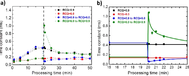
3.3 Time constant of the anodic voltage-time responses
Concerning the voltage-time response recorded over one pulse period of the anodic current,
chronograms in Fig. 2 show that the voltage signal exhibits a transient regime during the first
milliseconds following the beginning of the anodic pulse. The duration of this transient regime
may be short or long, depending on the applied electrical conditions. As reported in a previous
study, the experimental data of the anodic voltage-time response were adequately fitted by an
exponential function giving access to the time constant of this transient regime [19]. In parallel with these chronograms, Fig. 4 reports the evolution of this time constant (noted ) as a function of the processing time for each PEO treatment performed. At the beginning of the process (at 1 min), and irrespective of the investigated conditions, the time constant is low (less than 0.1 ms). Until the switching point that will occur at 20 min, Fig. 4 shows that the time constant
gradually increases with the processing time. It increases more rapidly using the low RCQ
constant is long and reaches 0.43 ms for the treatment performed with the low RCQ while it remains short and reaches only 0.16 ms for the treatment conducted with the high RCQ. In addition, it is also worth noting that the evolutions of the delay t (Fig. 3) and the time constant (Fig. 4) for the different RCQ investigated are similar which is in good agreement with previous observations [19].
Right after 20 min, Fig. 4b evidences that the time constant suddenly changes in different proportions depending on the sequenced treatment applied. When switching from the low RCQ
to the high one, the time constant behaves like the delay t in the MDs appearance since it suddenly drops from 0.43 ms to about 0.09 ms. Interestingly, the time constant reached right after the switching time is significantly lower than the time constant measured at the same
processing time with the corresponding reference treatment conducted with the high RCQ only ( = 0.16 ms). In addition and as already observed for the delay t, the opposite behaviour is strictly observed for the reverse sequence. Indeed, when the process switches from the high
RCQ to the low one, the time constant suddenly jumps from 0.16 ms to 1.06 ms. For this
specific sequenced treatment, the time constant reached right after the switching time is largely higher than the time constant measured at the same processing time with the corresponding reference treatment conducted with the low RCQ only ( = 0.43 ms). Finally, Fig. 4 evidences that after a certain period of time following the switching time - from a few to
tens of minutes depending on the sequenced treatment used - the time constant of the
voltage-time response tends to converge and to recover the value that it would have attained by using
the corresponding reference treatment.
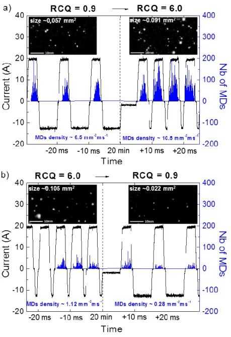
Fig. 5 shows the evolutions of the MDs characteristics (surface density and average size)
exactly at the time when the process switches from one RCQ to the second one. Fig. 5a is
associated to the sequenced treatment that switches from the low RCQ (RCQ = 0.9) to the high
RCQ (RCQ = 6.0) while Fig. 5b corresponds to the reverse sequence. Right before the
switching point that will occur at 20 min, MDs exhibit the same behaviour as that already
encountered in previous works e.g. numerous and small MDs are promoted with the low RCQ
while the high RCQ results in less numerous and bigger MDs [4, 16, 19]. In addition, and as
mentioned above concerning detection of the light emitted from the processed samples, Fig. 5
confirms that occurrence of the MDs is delayed with respect to the anodic current pulse, this
delay remaining higher for the high RCQ.
Right after 20 min, when the processes enter into the new RCQ, Fig. 5 evidences that
transition is associated with a sudden change in the MDs behaviour. Indeed, when the process
switches from the low RCQ to the high one, both the surface density and the average size of
the MDs suddenly increase from 6.5 mm-2ms-1 to 10.5 mm-2ms-1 and from 0.057 mm2 to 0.091 mm2, respectively. The opposite behaviour is strictly observed for the reversed sequence since both the surface density and the average size of the MDs suddenly decrease from 1.12 mm-2ms
-1 to 0.28 mm-2ms-1 and from 0.105 mm2 to 0.022 mm2, respectively. Said differently, numerous
and large MDs are promoted by switching from the low RCQ to the high one in the course of
the process while less numerous and smaller size MDs are promoted with the reverse sequence.
3.5 Morphology of the produced PEO coatings
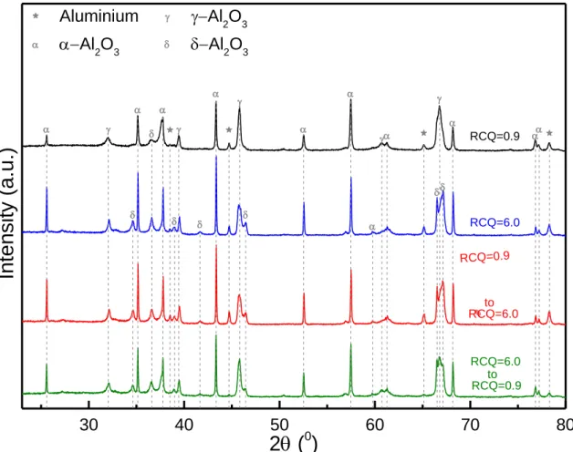
Figure 6 demonstrates XRD patterns of the produced oxide layers. Analysis of these
patterns shows that the coatings were mainly composed of α- and γ-phases of alumina. In
increasing with respect to γ-phase when high charge ratio is involved in the process, i.e. single
treatment with RCQ=6.0 and sequenced treatments. Moreover, transitional δ-phase was
observed, which also exhibited an increase in these cases. These findings are consistent with
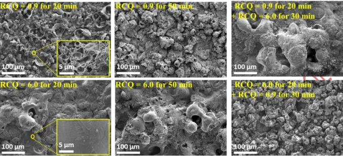
the existing literature [13]. SEM micrographs in Fig. 7 compare the top-surface views of the
different PEO coatings produced in the present study. All surfaces exhibit the typical
morphology of the PEO coatings consisting in “pancake”-like structures with voids of about 1
- 100 µm in diameter. These voids are usually associated with discharge channels that take
place during the PEO process [6, 12, 16]. This is particularly obvious for the oxide layer grown
for 20 min under the high RCQ which exhibits a “crater”-like structure with large voids up to
10 µm in diameter. In contrast, the use of the low RCQ for 20 min results in the formation of a “sponge”-like structure with fine open pores less than 1 µm in diameter. After 50 min processing time, these differences are much more pronounced. Moreover, Fig. 7 also shows
that the implementation of sequenced treatments has a significant effect on the morphology of
the top-most surface compared to the associated reference treatments. Interestingly, by
switching from the low RCQ to the high one, the fine “sponge-like” structure observed at 20
min turns into a rough “crater”-like structure at 50 min. The opposite morphological
transformation is strictly observed for the reverse sequence.
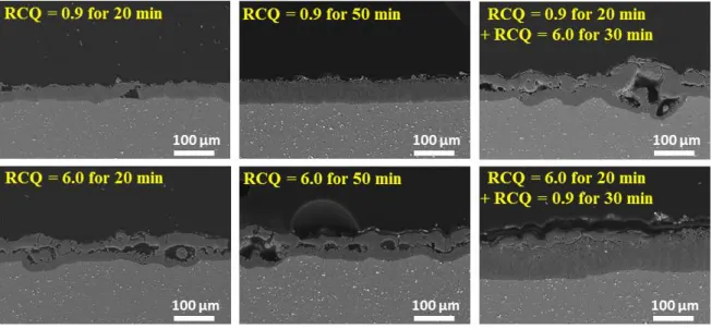
SEM micrographs in Fig. 8 shows the cross-sectional views of the different PEO coatings
produced in the present study. Moreover, and from a general point of view, the synthesized
oxide layers exhibit the typical morphology of PEO coatings consisting in two distinct regions,
more or less dependent on the processing conditions: a thick compact inner sublayer adjacent
to the aluminium substrate and a highly porous outer sublayer with large cavities. In parallel
with these cross-sectional views, Fig. 9 reports both the overall thickness of the oxide layer
(thickness of the inner and the outer sublayers) and the fraction of voids (up to 1 µm in
use of the high RCQ results in a thick overall coating (70 ± 5 µm) with large cavities through the outer sublayer (void fraction 13 ± 3 %) while the used of the low RCQ leads to a slightly thinner coating (62 µm ± 5 µm) much more compact (void fraction ~ 3 ± 3 %). Moreover, and as already observed from the top-surface views, Fig. 8 and Fig. 9 also put in evidence
that the use of sequenced treatments affect the final cross-sectional morphology of the
coatings compared to the associated reference treatments. The sequence treatment
involving the transition from the low RCQ to the high one has a detrimental effect on the morphology of the oxide layer. Indeed, although the overall thickness slightly increases (76 ± 5 µm), the fraction of voids significantly increases (12 ± 3 %) due to the presence of large cavities throughout the thickness. In contrast, the reverse sequence has a beneficial effect
on the morphology of the oxide layer since the overall thickness significantly increases (~ 109 ± 5 µm) while maintaining a low fraction of voids (~ 5 ± 3 %).
Fig. 10 compares the EDX element maps recorded on the cross-section of the samples
processed with the reference treatments performed for 50 min and with the specific sequenced
treatment (RCQ = 6.0 for 20 min followed by RCQ = 0.9 for 30 min) that provides the thickest
coating with a compact morphology. Whatever the applied conditions, the oxide layers
mainly contain Al, O, Si and K elements. Al comes from the Al2024 aluminium alloy
substrate while O, Si and K come from the electrolyte. EDX maps also evidence that Si
and K species are preferentially located throughout the outer porous sublayer while the inner
sublayer is mainly composed of Al and O. This observation is consistent with previous studies
that also evidenced that open cavities, in contact with the electrolyte, incorporate elements
from the electrolyte [39-41]. Nevertheless, some differences in the element distribution
throughout the oxide layer are significant when comparing the different treatments
investigated. In the case of the reference treatment conducted with the low RCQ, Si
the high RCQ. In the specific case of the sequenced treatment that switches from the high RCQ
to the low one, Si and K seem to be more concentrated and they are homogeneously distributed
throughout a thicker outer sublayer, which could certainly provide a better corrosion protection
of the aluminium alloy substrate. Indeed, some works that carried out PEO processes of
aluminium in electrolyte with various amount of diluted silicate have established that the
presence of such a silicon-rich barrier layer, mainly made of an amorphous silica SiO2 or
alumino-silica phase 3(AlO3)2(SiO2), improve both wear resistance and the corrosion
resistance of the aluminium alloys [39-41]. On that point, further corrosion experiments,
mainly conducted via electrochemical impedance spectroscopy, should be devoted to verify a
potential enhancement of the corrosion resistance of the samples processed with sequenced
treatments, especially the one that switches from the high to the low RCQ.
4. Discussion
The present discussion focuses on the explanation of the experimental results by establishing
relationship between the optical characterization of the micro-discharges, the morphological
characterization of the produced PEO coatings and the various applied electrical conditions. In particular, making more explicit the link between the delay t in the MDs appearance, the time constant of the voltage-time response and the MDs properties is needed first to a better
understanding of the key role played by the MDs on the morphology of the growing oxide
layers. Finally, on the basis of the combined experimental results, the interest in using PEO
sequenced treatments will be discussed from the point of view of the energy consumption.
The schematic diagram in Fig. 11 shows the proposed mechanism of charge accumulation
that could explain the relationship between the delay ∆t in the MDs appearance, the time constant τ of the voltage-time response and the MDs properties, especially when the process suddenly switches from one RCQ to the second one in the course of the PEO treatment.
At the beginning of the process, results have shown that the delay in the MDs appearance
- correlated to the time constant of the voltage-time response – gradually increases with
the processing time (Fig. 3 and Fig. 4). It also increases more rapidly using the low RCQ than
the high one. It was previously established that the ratio of charge quantity controls the
dynamic of establishment of a stable electrical double layer (EDL) at the electrolyte / oxide
interface, which in turn, once established, governs the dielectric breakdown of the oxide
layer and therefore the ignition of the MDs [19]. The dynamic of establishment of this EDL
is mainly affected by the mechanism of charge accumulation taking place at the interface
between the oxide and the electrolyte. Depending on the substrate bias polarization, charges
(cations (H+) and anions (OH-) that are expected to be the most important species in terms of number density and mobility) are accumulated at this interface during the anodic alternation
of the current pulse while they are relaxed during the cathodic one. When processing with
high RCQ (RCQ = 6.0) value, the low magnitude of the cathodic part (i.e. the combined
effects of a low cathodic current amplitude and/or a short duration resulting in a low cathodic charge quantity) doesn’t allow the complete relaxation of charges accumulated during the previous anodic alternation of the current. So, charges remain close to the interface
and they accumulate much more rapidly during the subsequent anodic alternation. It results
that the time needed to accumulate charge is short and breakdown occurs earlier with a short
delay between the applied anodic current and the MDs appearance. It gives rise to large and
long-lived MDs. In contrast, with the low RCQ - the amplitude of the cathodic current
and the cathodic part duration being higher compared to the high RCQ – charges
relaxed during the subsequent cathodic alternation and the accumulation mechanism restarts at
each new anodic alternation. It results that the time needed to accumulate charge is long and
breakdown occurs later with a long delay between the applied anodic current and the MDs
appearance. In this case, it gives rise to small and short-lived MDs. Moreover, the fact that both
the delay in the MDs appearance and the time constant of the voltage-time response gradually
increase with the processing time is explained by taking into account some evolutions in the
morphological aspects of the growing oxide layer, particularly its gradual thickening and the
development of fine porosities, the latter exhibiting a higher specific area and a higher charge
storage capacity. As the process goes on, more accumulated charges are therefore needed to
reach the dielectric breakdown voltage of the growing oxide layer resulting in a longer delay t and in a longer time constant .
Right before the switching point, although the oxide layer elaborated with the low RCQ
remains quite compact - no large cavities up to 10 µm in diameter are visible throughout the
thickness -, SEM observations have revealed the presence of a fine “sponge”-like structure with
very small porosities less than 1 µm in diameter at the top-most surface (Fig. 7). This
sponge-like structure exhibits a high specific area associated with a high charge storage capacity. In
this case, right before the switching point, the accumulation of charges at the oxide / electrolyte
interface is therefore mainly limited due to two joint effects e.g. the application of a low RCQ
(high extraction of electric charges during the high magnitude of the cathodic regime) to a “sponge”-like top-most surface (high dispersion of charges through the fine porosities filled with the conductive electrolyte) (Fig. 11a). This explains why, right before the switching point,
the delay in the MDs appearance and the time constant of the voltage-time response reached
high values (Fig. 3 and Fig. 4). It is also in good agreement with experimental results on the
MDs behaviour which are numerous and but with small size (Fig. 5) since they are finely
sample processed for 20 min with the high RCQ have revealed large open cavities up to 10 µm
in diameter throughout the outer oxide sublayer but no fine porosities at the top-most surface
(Fig. 7). Contrary to the “sponge”-like structure that develops under the low RCQ, this
“crater”-like structure presents a lower specific area and a lower charge storage capacity. In this case,
right before the switching point, the accumulation of charges is therefore strong due to the
combined effects of a high RCQ (low extraction of electric charges during the low magnitude
of the cathodic regime) and the thinness of the inner compact oxide sublayer underneath the
open cavities (Fig. 11b). This explains why the delay in the MDs appearance and the time
constant of the voltage-time response remains short with the development of fewer MDs with
larger size.
Interestingly, by suddenly switches the RCQ in the course of the process, the results have
evidenced that the delay in the MDs appearance, the time constant of the voltage-time response
and the MDs behaviour also suddenly change in opposite proportions depending on the
sequenced treatment applied. If the electrical condition suddenly changes from the low RCQ
to the high one, the previous oxide layer grown under the low RCQ – known to exhibit a
sponge-like structure as previously discussed - is thus suddenly submitted to the high RCQ. In
this case, right after the switching point, the electrical and the morphological conditions are
met to promote the strongest and the most rapid accumulation of charges at the oxide /
electrolyte interface. Indeed, on one hand, the dynamic of charge extraction from the surface
suddenly becomes low due to the low magnitude of the cathodic current alternation, and, in
other hand, the number of charges involved is high due to the high storage charge capacity of
the sponge-like structure. As a consequence, and as illustrated in Fig. 11a, the MDs appears
quite instantaneously with the rising edge of the anodic current that is in good agreement with
the sudden drop of the delay in the MDs appearance and the time constant of the transient
time constant reached lower values than the values obtained at the same processing time within
the corresponding single treatment conducted at high RCQ. In addition, when the process
suddenly turns into the new RCQ, the accumulation of charge becomes so strong that it results
in the development of numerous and large-size MDs. MDs are numerous due to the fact that
they develop throughout the network of fine porosities at the top-most surface of the oxide
layer. For a similar reason, and as illustrated in Fig. 11b, if the electrical conditions suddenly
change from high to low RCQ, the mechanism of charge accumulation becomes inhibited by
the combined effects of a high extraction of electric charges due to the high magnitude of the
cathodic current alternation and by the limited number of charges involved in this dynamic of
charge accumulation due to the lower storage capacity of the “crater”-like structure.
Consequently, the dielectric breakdown is strongly delayed explaining why the delay in the
MDs appearance and the time constant of the voltage-time response remains short, largely
lower than the values obtained at the same processing time within the corresponding reference
treatment at high RCQ (Fig. 3 and Fig. 4). Finally, for this specific sequenced treatment, the
mechanism of charge accumulation is so inhibited at the oxide / electrolyte interface by the
aforementioned causes that it gives rise to smoother MDs as experimentally observed (few and
small-size MDs right after the switching point in Fig. 6).
4.2 PEO coatings improvement
Results clearly evidenced that the implementation of sequenced treatments have a
significant effect on the coatings morphology compared to the associated reference treatments.
These effects can be explained by considering the previous explanations on the relationship
between the delay in the MDs appearance, the time constant of the voltage-time response and
The sequenced treatment that switches from the high to the low RCQ value results in the
thickest coating (109 µm) combined with a low fraction of voids (5 vol. %). Within this specific
sequenced treatment, it is as if the thick overall oxide layer (~ 53 µm) formed during the first
sequence (RCQ = 6.0 for 20 min in Fig. 8) is kept while the large cavities formed (up to 10 µm
in diameter) are completely filled with alumina during the second sequence. These observations
can be explained by considering the earlier transition into the beneficial "soft" regime during
which the processed sample experiences smoother MDs regarding both their limited number
over the processed surface and their smaller size (Fig. 5b). During this “soft” regime, Cheng et
al. [30, 31] also proposed the ignition of internal D-type MDs that are expected to occur in the
pancake-like cavities allowing these cavities to be gradually filled with solidified alumina. Said
differently, the experimental results seem to support a repairing mechanism taking place inside
the large cavities of the thick oxide layer elaborated during the first sequence at high RCQ.
When the process switches to the low RCQ, this mechanism is suddenly triggered and,
simultaneously, experimentally confirmed by the sudden changes in the MDs behaviour, the
latter becoming less numerous (~ 0.28 mm-2ms-1) with smaller average size (~ 0.022 mm2) due to the low aforementioned mechanism of charge accumulation at the oxide / electrolyte
interface (Fig. 5b).
In contrast, results have shown that the reverse sequenced treatment involving the transition
from the low to the high RCQ value has detrimental effects on the produced oxide layer. Indeed,
although the thickness of the overall oxide layer is slightly higher than that produced with the
reference treatment at low RCQ for 50 min, larger cavities are even visible throughout the
coating providing a more irregular and rugged aspect of the top most surface (Fig. 8). Within
this specific sequenced treatment, the preformed during the first sequence layer (RCQ = 0.9
for 20 min) is further grown, not only developing large cavities, but also at times deteriorating
observe that porosities have been enlarged and cracks have appeared in the sublayer of the
sequenced sample (RCQ=0.9 to RCQ=6.0), compared to RCQ=0.9 for 20 min. Moreover, large
cavities have been developed in the vicinity of the oxide/substrate interface, as a result of strong
B-type micro-discharges, taking place throughout the total of the oxide layer. The presence of
such large cavities that are usually considered as discharge channels is directly correlated with
the MDs behaviour (Fig. 5). Indeed, switching from the low to the high RCQ value is associated
with the sudden ignition of more numerous and larger-size MDs due to the strong
aforementioned mechanism of charge accumulation at the oxide / electrolyte interface (Fig.
11).
4.3 Energy saving with PEO sequenced treatments
If a sequenced treatment starts with the high RCQ value (typ. > 1), and is then followed with
the low RCQ in the range of [0.8 – 1], a thick coating with large cavities grows under strong
MDs (numerous and large size MDs) during the first sequence. Then, the switching to the second sequence triggers earlier the low energy consumption “soft” regime associated with the ignition of smoother micro-discharges (less numerous and smaller size MDs). As the process
goes on, the high thickness previously achieved during the first sequence is maintained and
continues to grow while the large porosities are gradually filled with crystalline alumina
enriched of elements from the electrolyte (mainly Si) (that could probably provide better
corrosion and wear resistance). Consequently, using this virtuous sequenced treatment, the
produced oxide layer is the thickest and the most compact and needs the lowest energy to grow.
By this way, and as summarized in Table 1, the specific energy consumption which is defined
as the electrical energy used to grow 1 µm coating over 1 m2 proves to be the lowest (13 kWh.m
single treatment performed under the beneficial “soft”-regime conditions (RCQ = 0.9 during 50 min), the growth rate can be increases by ∼ 40 % while maintaining a low level of porosity (~ 5 %). Interestingly, this improvement is not made at the expense of energy consumption
that is actually reduced by ∼ 35 %.
In contrast, if a sequenced treatment starts with the low RCQ value (0.8 < RCQ < 1) and
then is followed with the high one (> 1), a thin but dense oxide layer is synthesised during the
first sequence under small-size MDs. When switching to the second sequence, an “arcs” regime is triggered and more numerous and larger-size MDs are ignited. Entering into the “arcs” regime that is energy consuming, the previous dense layer developed during the first sequence is gradually damaged with the formation of large open pores that are known
to degrade the wear and corrosion resistance. Therefore, and as resumed in Table 1, the
specific energy consumption increases (17 kWh.m-2.µm-1).
4. Conclusion
The present works investigated the effects of sequenced treatments on the plasma
electrolytic oxidation (PEO) of aluminium. The main conclusions are given hereafter.
Firstly, the singular variations of the delay in the micro-discharges appearance and the time constant of the voltage-time response were explained by a mechanism of charge
accumulation taking place through the electrical double layer (EDL) located at the
oxide/electrolyte interface. It was established that this mechanism depends not only on the
applied electrical conditions, but is also affected by the morphology of the growing oxide,
particularly by the specific surface area in contact with the electrolyte.
Secondly, a synergetic effect was observed when combining a high, at first, and a low, afterwards, ratio of charge quantity (RCQ). It resulted to a significant enhancement of the
produced coating, by increasing the total thickness and, simultaneously, maintaining a
compact and dense structure of the oxide layer.
Finally, this specific PEO sequenced treatment, despite including a high RCQ at first, resultedin a significant decrease (by 35 %) in total energy consumption compared to any
other treatment investigated. The use of PEO sequenced treatments opens opportunities for
Acknowledgments
This work was supported by the French Government through the program "Investissements d’avenir" operated by the French National Research Agency (ANR) and referenced to as ANR-11-LABX-0008-01 (LabEx DAMAS).
The authors would like to acknowledge contribution of the following:
- the competence cluster on electron microscopy at IJL for providing advices in SEM observations and analyses.
- Dr. F. Brochard and APREX Solution company for their help in providing and adapting the TRACE software to our requirement for quantifying and analysing the micro-discharges.
Data availability
The data that support the findings of this study are available from the corresponding author, JM, upon reasonable request.
Contribution of each author
G.H., J.M. and A.N. conceived the experiments.
V.N. and J.M. conducted the experiments.
V.N., J.M. and A.N. performed the in-situ optical process diagnostic.
V.N. and J.M. performed all SEM analyses and interpretations. All the authors analysed the results.
V.N. and J.M. prepared the manuscript while all authors reviewed the manuscript.
References
[1] A.L. Yerokhin, X. Nie, A. Leyland, A. Matthews, S.J. Dowey, Plasma electrolysis for
surface engineering, Surf. Coat. Technol. 122 (1999) 73-93.
[2] E. Matykina, A. Berkani, P. Skeldon, G.E. Thompson, Real-time imaging of coating growth
during plasma electrolytic oxidation of titanium, Electrochim. Acta 53 (2007) 1987-1994.
[3] F. Jaspard-Mécuson, T. Czerwiec, G. Henrion, T. Belmonte, L. Dujardin, A. Viola, J. Beauvir, Tailored aluminium oxide layers by bipolar current adjustment in the Plasma
Electrolytic Oxidation (PEO) process, Surf. Coat. Technol. 201 (2007) 8677-8682.
[4] J. Martin, A. Melhem, I. Shchedrina, T. Duchanoy, A. Nominé, G. Henrion, T. Czerwiec, T. Belmonte, Effects of electrical parameters on plasma electrolytic oxidation of aluminium, Surf. Coat. Technol. 221 (2013) 70-76.
[5] L. R. Krishna, A. S. Purnima, G. A. Sundararajan, comparative study of tribological
behavior of microarc oxidation and hard-anodized coatings. Wear 261 (2006) 1095–1101.
[6] K. Tillous, T. Toll-Duchanoy, E. Bauer-Grosse, L. Hericher, G. Geandier, Microstructure
and phase composition of microarc oxidation surface layers formed on aluminium and its alloys 2214-T6 and 7050-T74. Surf. Coat. Technol. 203 (2009) 2969–2973.
[7] L.O. Snizhko, A.L. Yerokhin, A. Pilkington, N.L. Gurevina, D.O. Misnyankin, A. Leyland, A. Matthews, Anodic processes in plasma electrolytic oxidation of aluminium in alkaline
solutions, Electrochim. Acta 49 (2004) 2085-2095.
[8] H. F. Guo, M.Z. An, H.B. Huo, S. Xu, L.J. Wu, Microstructure characteristic of ceramic
coatings fabricated on magnesium alloys by micro-arc oxidation in alkaline silicate solution,
[9] Q. Cai, L. Wang, B. Wei, Q. Liu, Electrochemical performance of microarc oxidation films
formed on AZ91D magnesium alloy in silicate and phosphate electrolytes, Surf. Coat. Technol.
200 (2006) 3727-3733.
[10] C. Blawert, V. Heitmann, W. Dietzel, H.M. Nykyforchyn, M. Klapkiv, Influence of
electrolyte on corrosion properties of plasma electrolytic conversion coated magnesium alloys,
Surf. Coat. Technol. 201 (2007) 8709-8714.
[11] J. Liang, P. Bala Srinivasan, C. Blawert, M. Störmer, W. Dietzel, Electrochemical
corrosion behaviour of plasma electrolytic oxidation coatings on AM50 magnesium alloy formed in silicate and phosphate based electrolytes, Electrochim. Acta 54 (2009) 3842-3850.
[12] A.L. Yerokhin, A. Shatrov, V. Samsonov, P. Shashkov, A. Pilkington, A. Leyland, A. Matthews, Oxide ceramic coatings on aluminium alloys produced by a pulsed bipolar plasma
electrolytic oxidation process, Surf. Coat. Technol. 199 (2005) 150-157.
[13] E. Matykina, R. Arrabal, P. Skeldon, G.E. Thompson, Investigation of the growth
processes of coatings formed by AC plasma electrolytic oxidation of aluminium, Electrochim.
Acta 54 (2009) 6767-6778.
[14] E.V. Parfenov, A. Yerokhin, A. Matthews, Small signal frequency response studies for
plasma electrolytic oxidation, Surf. Coat. Technol. 203 (2009) 2896-2904.
[15] P. Bala Srinivasan, J. Liang, R.G. Balajeee, C. Blawert, M. Störmer, W. Dietzel, Effect of
pulse frequency on the microstructure, phase composition and corrosion performance of a phosphate-based plasma electrolytic oxidation coated AM50 magnesium alloy, Appl. Surf. Sci.
256 (2010) 3928-3935.
[16] A. Melhem, G. Henrion, T. Czerwiec, J.L. Briançon, T. Duchanoy, F. Brochard, T. Belmonte, Changes induced by process parameters in oxide layers grown by the PEO process
[17] R.O. Hussein, D.O. Northwood, X. Nie, The influence of pulse timing and current mode
on the microstructure and corrosion behaviour of a plasma electrolytic oxidation (PEO) coated AM60B magnesium alloy, J. Alloys Comp. 541 (2012) 41-48.
[18] A. V. Timoshenko and Y. V. Magurova, Investigation of plasma electrolytic oxidation
processes of magnesium alloy MA2-1 under pulse polarisation modes, Surf. Coat. Technol.,
199 (2005) 135–140.
[19] J. Martin, A. Nominé, F. Brochard, J-L. Briançon, C. Noël, T. Belmonte, T. Czerwiec, G.
Henrion, Delay in micro-discharges appearance during PEO of Al: Evidence of a mechanism
of charge accumulation at the electrolyte / oxide interface. Appl. Surf. Sci. 410 (2017) 29-41.
[20] M.D. Klapkiv, State of an electrolytic plasma in the process of synthesis of oxides based
on aluminum, Mater. Sci. 31 (1996) 494-499.
[21] M.D. Klapkiv, Simulation of synthesis of oxide-ceramic coatings in discharge channels of
a metal-electrolyte system, Mater. Sci. 35 (1999) 279-283.
[22] G. Sundararajan, L. Rama Krishna, Mechanisms underlying the formation of thick alumina
coatings through the MAO coating technology, Surf. Coat. Technol. 167 (2003) 269-277.
[23] L.R. Krishna, A.S. Purnima, N.P. Wasekar, G. Sundararajan, Kinetics and Properties of
Micro Arc Oxidation Coatings Deposited on Commercial Al Alloys, Metall. Mater. Trans. A
38 (2007) 370-378.
[24] A.L. Yerokhin, V.V. Lyubimov, R.V. Ashitkov, Phase formation in ceramic coatings
during plasma electrolytic oxidation of aluminium alloys, Ceram. Int. 24 (1998) 1-6.
[25] E. Matykina, R. Arrabal, D.J. Scurr, A. Baron, P. Skeldon, G.E. Thompson, Investigation
of the mechanism of plasma electrolytic oxidation of aluminium using 18O tracer, Corr. Sci. 52
[26] R.O. Hussein, X; Nie, D.O. Northwood, A. Yerokhin, A. Matthews, Spectroscopic study
of electrolytic plasma and discharging behaviour during the plasma electrolytic oxidation (PEO) process, J. Phys. D.: Appl. Phys. 43 (2010) 105203.
[27] R.O. Hussein, X. Nie, D.O. Northwood, An investigation of ceramic coating growth
mechanisms in plasma electrolytic oxidation (PEO) processing, Electrochim. Acta 112 (2013)
111-119.
[28] J. Jovović, S. Stojadinović, N.M. Šišović, N. Konjević, Spectroscopic characterization of
plasma during electrolytic oxidation (PEO) of aluminium, Surf. Coat. Technol. 206 (2011)
24-28.
[29] V. Dehnavi, B.L. Luan, D.W. Shoesmith, X.Y. Liu, S. Rohani, Effect of duty cycle and
applied current frequency on plasma electrolytic oxidation (PEO) coating growth behaviour,
Surf. Coat. Technol. 226 (2013) 100-107.
[30] Y. Cheng, F. Wu, E. Matykina, P. Skeldon, G.E. Thompson, The influences of
microdischarge types and silicate on the morphologies and phase compositions of plasma electrolytic oxidation coatings on Zircaloy-2, Corr. Sci. 59 (2012) 307-315.
[31] Y. Cheng, Z. Xue, Q. Wang, X. Wu, E. Matykina, P. Skeldon, G.E. Thompson, New
findings on properties of plasma electrolytic oxidation coatings from study of an Al–Cu–Li alloy, Electrochim. Acta 107 (2013) 358-378.
[32] Y. Cheng, M. Mao, J. Cao, Z. Peng, Plasma electrolytic oxidation of an Al-Cu-Li alloy in
alkaline aluminate electrolytes: A competition between growth and dissolution for the initial ultra-thin films, Electrochim. Acta 138 (2014) 417-429.
[33] A. Nominé, A. V. Nominé, N. St. J. Braithwaite, T. Belmonte, G. Henrion,
High-Frequency-Induced Cathodic Breakdown during Plasma Electrolytic Oxidation, Phys. Rev.
[34] A. B. Rogov, A. Yerokhin, A. Matthews, The role of cathodic current in plasma
electrolytic oxidation of aluminum: Phenomenological concepts of the “soft sparking” mode,
Langmuir, 33 (2017), 11059 – 11069.
[35] A.B. Rogov, V.R. Shayapov, The role of cathodic current in PEO of aluminium: influence
of cationic electrolyte composition on the transient current voltage curves and the discharges optical emission spectra, Appl. Surf. Sci. 394 (2017) 323-332.
[36] S. Bardin, J-L. Briançon, F. Brochard, V. Martin, Y. Zayachuk, R. Hugon, J. Bougdira,
Investigating transport of dust particles in plasmas, Contrib. Plasma Phys. 51 (2011) 246-
251.
[37] N. Endstrasser, F. Brochard, V. Rohde, M. Balden, T. Lunt, S. Bardin, J.-L. Briançon, R. Neu, Video tracking and post-mortem analysis of dust particles from all tungsten ASDEX
Upgrade, J. Nucl. Mater. 415 (2011) S1085-S1088.
[38] A. Nominé, J. Martin, C. Noël, G. Henrion, T. Belmonte, I.V. Bardin, P. Lukès, Surface
charge at the oxide/electrolyte interface: Toward optimization of electrolyte composition for treatment of Aluminum and Magnesium by Plasma Electrolytic Oxidation, Langmuir 32 (2016)
1405–1409.
[39] V. Dehnavi, D. W. Shoesmith, B. L. Luan, M. Yarid, X. Y. Liu, S. Rohani, Corrosion
properties of plasma electrolytic oxidation coatings on an aluminium alloy – The effect of the PEO process stage, Mater. Chem. Phys. 161 (2015) 49-58.
[40] A. Ghasemi, V.S. Raja, C. Blawert, W. Dietzel, K.U. Kainer, The role of anions in the
formation and corrosion resistance of the plasma electrolytic oxidation coatings, Surf. Coat.
Technol. 204 (2009) 1469-1478.
[41] A. Polat, M. Makaraci, M. Usta, Influence of sodium silicate concentration on structural
and tribological properties of microarc oxidation coatings on 2017A aluminum alloy substrate,
List of tables
Table 1: Parameters of current waveforms used for RCQ = 0.9 and RCQ = 6
RCQ Qp (mC) Qn (mC) Waveform
0.9 61 68.4
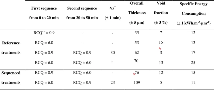
Table 2: PEO treatments performed with the associated time of the “soft” regime appearance,
the average thickness and the porosity of the overall PEO coatings and the specific energy
consumption. First sequence from 0 to 20 min Second sequence from 20 to 50 min tSR* ( 1 min) Overall Thickness ( 5 µm) Void fraction ( 3 %) Specific Energy Consumption (± 1 kWh.m-2∙µm-1) Reference treatments RCQ** = 0.9 - - 35 7 12 RCQ = 6.0 - - 53 15 13 RCQ = 0.9 RCQ = 0.9 30 62 3 17 RCQ = 6.0 RCQ = 6.0 - 70 13 25 Sequenced treatments RCQ = 0.9 RCQ = 6.0 - 76 12 15 RCQ = 6.0 RCQ = 0.9 23 109 5 11
*tSR = Time of the “soft” regime appearance
List of figures
Figure 1: Time evolution of the anodic voltage amplitude for the different conditions
investigated and summarized in Table 1. The vertical dash line (---) indicates the switching
time of the RCQ conditions. Stars (*) indicate the time at which the process enters into the “soft” regime. 0 10 20 30 40 50 0 200 400 600 800
*
Anodic voltage amplitude (
v)
Processing time (min)
RCQ=0.9 RCQ=6.0 RCQ=0.9 to RCQ=6.0 RCQ=6.0 to RCQ=0.9*
16 18 20 22 24 500 600 700 800Figure 2: Evolution of the light emission (blue lines) with the corresponding current (black
lines) and voltage (red lines) signals recorded over 10 ms for the sequenced PEO treatments
investigated and summarized in Table 1. The vertical dash line (---) indicates the switching
Figure 3: a) Evolution of the delay of light emission as a function of processing time for the
different PEO processing conditions investigated and summarized in Table 1. The vertical dash
line (---) indicates the switching time of the RCQ conditions. b) Close-up of the delay evolution
Figure 4: a) Evolution of the time constant of the anodic voltage transient as a function of
processing time for the different PEO processing conditions investigated and summarized in
Table 1. The vertical dash line (---) indicates the switching time of the RCQ conditions. b)
²²²²²²²²²²²²²²
Figure 5: Evolution of the number of the micro-discharges (blue lines) that were detected using
fast video imaging with the corresponding current signal (black lines) recorded exactly when
the PEO process switches from one RCQ to the second one (see Table 1). The vertical dash
line (---) indicates the switching time of the RCQ conditions. The insets are frames captured
from the movie of the processed sample recorded with fast video camera. a) For the sequenced
treatment that switches from the low RCQ = 0.9 to the high RCQ = 6.0. b) For the sequenced
30 40 50 60 70 80 RCQ=6.0 RCQ=0.9 RCQ=6.0
Int
en
sity (a
.u.
)
2 (
0)
Aluminium Al 2O3 Al 2O3 Al2O3 RCQ=0.9 to RCQ=6.0 to RCQ=0.9Figure 6: XRD patterns of the oxide coatings produced under different conditions.
Figure 7: SEM top-surface views of the PEO oxide layers elaborated under the different PEO
Figure 8: SEM cross-sectional views of the PEO oxide layers elaborated under the different
62 70 76 109 3 13 12 5 RCQ=0.9 RCQ=6.0 RCQ=0.9 to 6.0RCQ=6.0 to 0.9 Thickness (+/- 5 µm) Void fraction (+/- 3%)
Figure 9: Measured thickness and estimated void fraction of the PEO oxide layers elaborated
for 50 min under the different PEO processing conditions investigated and summarized in
Figure 10: SEM cross-sectional views and the associated EDX element maps (Al, O, Si and
K) of the PEO oxide layers elaborated for 50 min with the reference treatments (RCQ = 0.9 and RCQ = 6.0) and with the sequenced treatment (RCQ = 6.0 for 20 min followed with RCQ
= 0.9 for 30 min)
RCQ = 0.9
RCQ = 6.0
RCQ = 6.0 to 0.9
Al
Al
Al
O
O
O
Si
Si
Si
K
K
K
Figure 11: Schematic model of combined effects of the ratio of charge quantity (RCQ) and
suddenly switches a) from a high RCQ (RCQ = 6.0) to a low RCQ (RCQ = 0.9) (blue line) and