HAL Id: hal-00859123
https://hal.archives-ouvertes.fr/hal-00859123
Submitted on 6 Sep 2013
HAL is a multi-disciplinary open access
archive for the deposit and dissemination of
sci-entific research documents, whether they are
pub-lished or not. The documents may come from
teaching and research institutions in France or
abroad, or from public or private research centers.
L’archive ouverte pluridisciplinaire HAL, est
destinée au dépôt et à la diffusion de documents
scientifiques de niveau recherche, publiés ou non,
émanant des établissements d’enseignement et de
recherche français ou étrangers, des laboratoires
publics ou privés.
of the Output Conductance and Transconductance in
AlInN/GaN HEMTs
Séraphin Dieudonné Nsele, Laurent Escotte, Jean-Guy Tartarin, Stéphane
Piotrowicz, Sylvain L. Delage
To cite this version:
Séraphin Dieudonné Nsele, Laurent Escotte, Jean-Guy Tartarin, Stéphane Piotrowicz, Sylvain L.
Delage. Broadband Frequency Dispersion Small Signal Modeling of the Output Conductance and
Transconductance in AlInN/GaN HEMTs. IEEE Transactions on Electron Devices, Institute of
Elec-trical and Electronics Engineers, 2013, 60 (4), pp. 1372-1378. �hal-00859123�
Abstract—Frequency dispersion of transconductance and output conductance in AlInN/GaN high electron mobility transistors is investigated in this paper. Broadband dispersion effects in the microwave frequency range are reported for the first time. A small-signal model is developed. Trapping effects are taken into account with parasitic electrical networks including distributed time constants. The model is compared to experimental data for several bias conditions and different types of dispersion.
Index Terms—AlInN/GaN HEMTs, dispersion effects, distributed time constants.
I. INTRODUCTION
lot of interest has been shown in recent years on nearly lattice-matched AlInN/GaN high electron mobility transistors (HEMTs) with a content of Indium of about 17% as very attractive devices for high-power amplifiers at microwave frequencies [1]. A record current gain cutoff frequency (fT) of 370 GHz is reported in [2] for a
30-nm-gate-length device. A maximum oscillation frequency (fMAX) of 220
GHz simultaneously obtained with fT of 205 GHz is also given
in [3] for the same gate-length value. Power amplifiers using AlInN/GaN HEMT technology on SiC substrate with a 0.25-µm-gate-length have been realized at X-band and K-band [4], [5], confirming the potential of this technology. Low-noise performance on 0.1-µm-gate-length HEMT is also reported in [6] with a minimum noise figure of around 0.6 dB at 10 GHz. The absence of strain in the AlInN/GaN heterostructure is beneficial for improving the reliability of the devices compared to conventional AlGaN/GaN transistors [7], [8].
In spite of these advantages, the AlInN/GaN technology suffers from an important gate leakage current dominated by Manuscript received December 4, 2012. This work was supported by the Genghis Khan project in the framework of the French Research National Agency (ANR).
S. D. Nsele, L. Escotte, and J.-G. Tartarin are with the Centre National de la Recherche Scientifique (CNRS), Laboratoire d’Analyse et d’Architecture des Systèmes (LAAS) and with Univ of Toulouse (UPS), F-31031, Toulouse, France.
S. Piotrowicz and S.L. Delage are with III-V Lab., 91460 Marcoussis, France.
Frenkel-Poole emission and from the presence of traps and threading dislocations [9]-[11]. Low-frequency dispersion of the output conductance attributed to trapping phenomena is also reported in [12]. The low-frequency dispersion of the output conductance or transconductance was largely investigated in GaAs MESFET and III-V HEMTs during the past (mainly up to 100 kHz) and a large bibliography can be found in the literature on this topic. It was also observed in AlGaN/GaN HEMTs and may be attributed to traps located in the GaN channel layer, at the AlGaN/GaN interface or at the surface area [13]-[16]. Trapping of carriers are generally responsible of parasitic effects, such as the virtual second gate [17], which directly impacts the power amplifiers characteristics [18], the noise properties [19], and the reliability of the devices [20].
In this work, we report a very broadband frequency dispersion of small-signal parameters in AlInN/GaN HEMTs up to microwave frequencies. The output conductance exhibits a positive frequency dispersion (i.e., it increases as the frequency grows) for all the bias conditions up to 1 GHz. The frequency dispersion of the transconductance is less pronounced, but both positive and negative dispersions are observed depending on the drain source voltage (VDS). The
very broadband nature of the dispersion suggests distributed time constants associated to trapping–detrapping effects, as mentioned by others [13], [15]. Based on S-parameter measurements versus bias and temperature conditions, we propose a small-signal model including parasitic networks which takes into account the different behaviors experimentally observed. An analytical model, which could also be used in the low-frequency range, is employed to describe the distribution of time constants. This model is very useful to improve the physics-based knowledge of these effects and can provide a valuable feedback to improve the technology currently under development.
II. DEVICE AND EXPERIMENTAL SETUP
A. Device technology
A cross-sectional schematic of the AlInN/GaN HEMT is presented in Fig.1. The layers are grown on a SiC substrate. The heterostructure consists of a 1.7-µm-thick insulating GaN
Broadband Frequency Dispersion Small Signal
Modeling of the Output Conductance and
Transconductance in AlInN/GaN HEMTs
Séraphin Dieudonné Nsele, Laurent Escotte, Jean-Guy Tartarin, Stéphane Piotrowicz, and Sylvain L.
Delage
buffer layer, followed by a 1-nm-thick AlN spacer layer and a 11.5-nm-thick AlInN layer with 18.7% of Indium content. The device is passivated with a 250-nm-thick Si3N4 layer. The gate
length is 0.25 µm and the total gate width is 150 µm. The gate-source and gate-drain distances are 0.5 and 2 µm, respectively. The details of the epitaxial and technological processes can be found in [5].
B. Experimental setup
On-wafer measurement results reported in this paper were realized using an automatic vector network analyzer (ZVRE, Rohde & Schwarz). S-parameters have been measured between 100 kHz and 4 GHz. The low-frequency value of the experimental setup is limited by the bias tees. Short open load thru (SOLT) method is used to calibrate the network analyzer. Temperature measurements are realized using a cryoprober (PMC200, Süss Microtec). Additional S-parameter measurements have been done up to 40 GHz (with NE5230C, Agilent) to determine the extrinsic elements of the equivalent circuit. Finally, the Y-parameters have been calculated and transferred to a circuit simulator. It is difficult to separate thermal effects from trapping effects with electrical measurements since both are temperature dependent. All the measurements are realized when the transistor is thermally stabilized corresponding to a stable drain current. Thermal effects with large time constants are then minimized.
III. EXPERIMENTAL RESULTS
A. Output conductance dispersion
The real part of Y22 divided by the measured value at 100
kHz (output conductance ratio) is plotted in Fig. 2 versus frequency for several values of VDS. The gate-source-voltage
(VGS) is equal to –1 V. A positive dispersion is observed for all
bias conditions. For VDS values below 10 V the dispersion is
less than 33%. A large increase is observed for VDS values
greater than 13 V. We report a ratio of 500% and 1700% at
VDS = 15 V and 17 V, respectively. The imaginary part of Y22
versus frequency is shown in Fig.3. The positive values indicate a capacitive behavior of the output impedance and the different peaks strongly depend on VDS. At high-field values, a
large peak appears between 100 kHz and 1 MHz, which is shifted toward high frequencies when VDS grows. A time
constant () generally associated with a relaxation or trapping process is derived from the frequency value of the peak. The inset of Fig.3 reports the variations of the logarithm of versus the square root of VDS, along with a linear fit. This
corresponds to a typical field-assisted emission of trapped carriers, known as the Poole-Frenkel effect [21]. For VDS
values less than 10 V the time constant of this trap is increased and the corresponding peaks are out of the measurement
GaN: 1.7μm AlN: 1nm AlInN: 11.5nm 2DEG Si3N4: 250nm SiC Gate Drain Source
Fig. 1. Cross-section of the 0.25 µm AlInN/GaN HEMT. 0
2 4 6 8 10 12 14 16 18 Normaliz ed Outpu t C onducta nc e Frequency (Hz) 105 106 107 108 109 VDS=17 V VDS=15 V VDS=10 V VDS=13 V
Fig. 2. Frequency dispersion of the extrinsic output conductance. The data are divided by the values measured at 100 kHz with VGS = –1 V.
0.1 1.0 10.0 3.3 3.6 3.9 4.2 4.5 τ( μ s) VDS1/2 0 0.1 0.2 0.3 0.4 0.5 0.6 0.7 0.8 Im ag inar y part o f Y22 (m S) Frequency (Hz) VDS=10 V VDS=5 V VDS=3 V VDS=13 V VDS=15 V VDS=17 V 105 106 107 108
Fig. 3. Imaginary part of Y22 versus frequency measured at VGS = –1 V for several VDS values. The inset shows the variation of time constants versus the square root of VDS. 0 0.1 0.2 0.3 0.4 0.5 0.6 0.7 0.8 0.9 1 Im ag inar y par t of Y22 (mS) Frequency (Hz) 340 K 300 K 200 K 105 106 107 108
Fig. 4. Imaginary part of Y22 versus frequency measured at VDS = 13 V and VGS = –1 V for several temperatures.
frequency range. The behavior of the output susceptance is also different because a broad peak is present for frequencies ranging from 1 MHz to 5 MHz. Fig.4 represents the variations of the imaginary part of Y22 versus frequency measured at VDS
= 13 V at three distinct temperatures, indicating that the field-assisted process is also thermally activated, in agreement with [21].
B. Transconductance dispersion
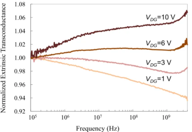
The real part of Y21 divided by the measured value at 100
kHz (transconductance ratio) is plotted in Fig. 5 versus frequency for several values of the drain-gate-voltage (VDG).
The frequency dispersion is not as significant as that of the output conductance and is less than 8% for all the investigated bias points. Several cases can be observed. For VDG less than 3
V, negative frequency dispersion is present in the whole frequency range. When VDG is increased, a positive dispersion
occurs at low-frequency and the negative dispersion disappears when VDG is greater than 6 V. This behavior was
described in GaN MESFETs [22]. The negative dispersion was observed and intensively studied in GaAs MESFETs at low-field values [23], [24] and in AlGaN/GaN HEMTs [14]-[16]. It is generally attributed to surface states in the ungated regions of the devices.
Dispersion effects are also observed on several 0.15-µm-gate-length devices issued from a different process. The broadband frequency behavior and the amplitude variations of the extrinsic parameters are globally the same as those reported in this paper. Moreover, the results exhibit a high degree of repeatability during an intensive characterization throughout five days.
IV. MODELING
A. Small-signal model including a single trap
Fig. 6 represents the simplified intrinsic small-signal model of the transistor including dispersion effects when only a single trap is considered [25]. Cgs, gm, and gd represent the
gate-source capacitance, the transconductance, and the output conductance, respectively. The dispersion effects are taken
into account with the parasitic circuit where g0 and C0 are
parameters related to the modification of the channel conductance. The voltage-controlled-current-source (with transconductance gm0) is due to the detrapping current and is
frequency dependent. At high frequency, the trap cannot follow the AC voltage swing and this additional source is constant. The main difference of our model, compared to the one proposed by Golio et al. [25], is the command voltage (Vx), which can either be the gate-source-voltage (Vgs) or the
drain-gate-voltage (Vdg), depending on the type of dispersion.
The Y-parameters are given for each case by the following equations: 1) Vx = Vgs 0 0 0 21 g (g /g )Y Y m m (1) 0 22 g Y Y d (2) 2) Vx = Vdg 0 0 0 21 g (g /g )Y Y m m (3) 0 0 0 22 g (1 g /g )Y Y d m (4)
Y0 correspond to the admittance of the g0-C0 series-network
and is given by the following compact expression: 2 0 2 2 0 0 ) ( 1 ) ( ) ( 1 ) ( g j g Y (5)
= C0/g0 corresponds to the time constant of the process.
We have restricted the discussion to Y21 and Y22 because the
dispersion is not observed on Y11 and Y12. Case 1 corresponds
to the positive frequency dispersion of transconductance, whereas case 2 stands for the negative one. The minus sign in (3) indicates that detrapping current flows in opposite direction than 2DEG current, suggesting that the carriers are not the same. Equations (1) to (4) are well-adapted to describe the frequency dispersion behavior experimentally observed in Section III. The model can be extended to other situations if the sense of the parasitic current source is changed in the equivalent circuit. In that case, the Y-parameters are given by:
3) Vx = Vgs 0 0 0 21 g (g /g )Y Y m m (6) 0 22 g Y Y d (7) 4) Vx = Vdg 0 0 0 21 g (g /g )Y Y m m (8) 0 0 0 22 g (1 g /g )Y Y d m (9)
Equation (9) corresponds to the negative dispersion of the
0.92 0.94 0.96 0.98 1.00 1.02 1.04 1.06 1.08 No rma lized Ex trinsic T ransc onduc tanc e Frequency (Hz) VDG=6 V VDG=10 V VDG=3 V VDG=1 V 105 106 107 108 109
Fig. 5. Frequency dispersion of extrinsic transconductance. The raw data are divided by the values measured at 100 kHz. VDG = 1 V (VDS = 1 V, VGS = 0 V), VDG = 3 V (3 V,0 V), VDG = 6 V (5 V, –1 V), VDG = 10 V (10 V, 0 V).
Fig. 6. Intrinsic small-signal model including a single trap. The control voltage Vx could either be Vgs or Vdg.
output conductance (or to the inductive behavior of the output impedance) already observed elsewhere [26], [27].
It is well known that the access resistances could impact the extrinsic Y-parameter values. However, the intrinsic parameters (Y21 and Y22) are frequency-dependent and the
derivation of analytical relations becomes very tedious and differs from the aim of this paper.
B. Small-signal model including distributed time constants
Up to nine discrete parasitic networks, corresponding to 27 additional elements, are needed in some cases to obtain a good agreement with experimental data. The discrimination between the different trapping processes involved in the frequency dispersion is then difficult. The use of distributed time constants in the model is an alternative solution to reduce the number of parameters and to smooth the frequency response compared to a lumped approach.
Generation-recombination noise sources with a continuous distribution of time constants between 0 and 1 have been
proposed to explain the 1/f spectrum in semiconductors, assuming that the time constant distribution function, g(), is
given by [28]: ) / ( 1 ) ( 0 1 Ln g (10)
Ln stands for the Neperian logarithm. Equation (10) could
correspond to different possibilities [29]: carriers interacting by tunneling with traps spatially distributed at an interface, distribution in activation energies, or carriers interacting with acoustical phonons.
The model with a single trap is modified by integrating the expression of Y0 between 0 and 1:
d d d Y g d G jB Y0 1 0 ( ) 0 0 0 (11)
G0d and B0d correspond to the real and the imaginary parts
of the parasitic admittance (Y0d), respectively. This integral
can easily be solved and we get:
2 0 2 1 0 1 0 0 ) ( 1 ) ( 1 ) / ( 1 2 Ln Ln g G d (12)
( ) ( )
) / ( 1 0 1 0 0 0 Arctg Arctg Ln g B d (13)The Y-parameters of the intrinsic equivalent circuit can be obtained when Y0 is changed into Y0d in (1)–(4). The complete
small-signal model of AlInN/GaN HEMTs including extrinsic elements is represented in Fig.7. Trapping effects including distributed time constant is taken into account with the current source gmpVx associated with the parasitic admittance Y0d.
The transconductance gmp is given by:
d m
mp g g Y
g ( 0/ 0) 0 (14) Several networks can be added to correctly model the complex frequency behavior of the Y-parameters. The number of elements in the model is then increased. It requires the following strategy to extract the different values. The extrinsic transconductance is fitted to experimental data in a first step. The output conductance is then adjusted. Finally, the values of the different elements involved in the dispersion effects are refined in order to obtain simultaneously a good agreement for each parameter.
V. RESULTS AND DISCUSSION
Fig.8 represents the variations of the real part of the transconductance versus frequency at VDS = 3 V for several
values of VGS. The plots are normalized with respect to the
low-frequency values. Very good agreement between the model and experimental data is observed for different bias conditions. A total of four parasitic networks are used to model at the same time both Y21 and Y22, indicating that
several trapping processes are present in the device. Two current sources are controlled by Vgs and the others are
controlled by Vdg. This behavior is the most complicated to
describe because opposite processes (i.e. positive and negative dispersions) are present and can cancel each other out, as shown at VGS = 0 V in the low-frequency range. At VGS = –1.5
V (VDG = 4.5 V), the negative dispersion is reduced and only
one current source controlled by Vdg is used. This could be due
to an extension of the space charge region in the gate-drain region which reduces the number of trapped carriers. The variations of the transconductance versus frequency measured at VGS = –1 V for several values of VDS larger than 10 V are
reported in Fig.9. In this case, the negative dispersion has disappeared and four parasitic networks with current sources controlled by Vgs are used. These additional parasitic networks
are correlated to the apparition in the measured frequency range of a field-assisted process. The positive frequency dispersion of the transconductance could be attributed to electron traps whereas the negative frequency dispersion could be due to hole traps at the surface as demonstrated in GaAs MESFETs [30] and AlGaN/GaN HEMTs [16] using two-dimensional numerical simulations. The values of the different elements extracted at VDS = 3V and VGS = –1 V are
given in Table 1 (extrinsic parameters), Table II (intrinsic parameters of the conventional model), and Table III (dispersion effects).
The variations of the output conductance versus frequency measured at VGS = –1 V for several values of VDS are presented
in Fig.10. The comparison with experimental data is presented in two different plots to appreciate the deviation between the calculated and measured values. At high field, the dispersion
gd gmVg s gm pVx Vd g Vg s Ri Rg d Cg s Cg d Cd s Y0d Rd Rg Lg Ld Ls Rs Cp g Cp d
P arasitic N etw ork Fig. 7. Small-signal model including one trap process with distributed time
is dominated by the Frenkel-Poole effect, as previously suggested. The corresponding value of the parasitic conductance g0 is largely higher than gd, which indicates the
presence of an additional conductive channel probably due to dislocations in the AlInN barrier layer. The time constants involved in the different processes cover a large range of values between 1 ns to 1 ms. The distribution of traps is in the range 0.5–10 Å, assuming a tunneling coefficient of 1010 m-1
[29]. It corresponds to a distribution of activation energies in the range 0.02–0.25 eV.
A good agreement between the model and experimental data is also observed on the imaginary parts of Y21 and Y22. A
similar agreement is obtained on the other Y-parameters (Y11
and Y12). Our results indicate that the proposed model is well
adapted to describe the frequency dispersion of AlInN/GaN HEMTs in several conditions. It could be used to understand the nature and the dynamic behavior of the trapping-detrapping processes. It could provide useful information on the physics of the frequency dispersion phenomena. Original expressions including distributed time constants are proposed in this way. The noise behavior of this technology is currently under investigation and the small-signal model proposed in this paper will be used to study the noise sources in GaN
devices in the presence of generation-recombination centers. Nonlinear modeling of GaN transistors in the presence of dispersion effects is currently a critical issue: our approach stands as the first step to include these effects in a complete
0.98 1 1.02 1.04 1.06 1.08 1.1 1.12 Normaliz ed Ex trinsic T ra nsco nductance Frequency (Hz) 105 106 107 108 109 VDS=10 V, 13 V, 15 V, 17 V
Fig. 9. Extrinsic Transconductance versus frequency at VGS = –1 V for several values of VDS. The plots are normalized with respect to the values at 100 kHz. Full-lines: measured data. Dotted-lines: model.
0.97 0.98 0.99 1 1.01 1.02 1.03 Normaliz ed Ex tr in sic T ransconductanc e Frequency (Hz) VGS =0 V, −0.5 V, −1 V, −1.5 V 105 106 107 108 109
Fig. 8. Extrinsic transconductance versus frequency at VDS = 3 V for several values of VGS. The plots are normalized with respect to the values at 100 kHz. Full-lines: measured data. Dotted-lines: model.
0.9 1 1.1 1.2 1.3 1.4 N orm al iz ed Out put Conduct ance Frequency (Hz) 105 106 107 108 109 VDS=10 V VDS=5 V VDS=3 V (a) 0 2 4 6 8 10 12 14 16 18 Nor m aliz ed Output Conduc tance Frequency (Hz) 105 106 107 108 109 VDS=13 V VDS=15 V VDS=17 V (b)
Fig. 10. Output conductance versus frequency at VGS= –1 V for several VDS values. The plots are normalized with respect to the values at 100 kHz. Full-lines: measured data. Dotted-Full-lines: model.
TABLEI
EXTRINSIC ELEMENTS OF THE SMALL-SIGNAL
Lg (pH) Ld (pH) Ls (pH) Rg () Rd () Rs () (fF) Cpg Cpd (fF) 133 110 1 5 9 5 46 36 TABLEII
INTRINSIC ELEMENTS OF THE SMALL-SIGNAL MODEL
VDS=3V AND VGS=–1V. gm (mS) (ps) gd (mS) Rgd () () Ri (fF) Cgs Cgd (fF) Cds (fF ) 32.6 0.28 12 9.3 1.2 132 56 99 TABLEIII
PARASITIC NETWORKS FOR FREQUENCY DISPERSION EFFECTS
VDS=3V AND VGS=–1V. Vx = Vgs Vx = Vdg gm0 (mS) 2.3 0.4 0.3 0.1 g0 (mS) 3.5 1 0.2 0.02 0 0.38 µs 11 ns 0.25 ns 0.12 µs 1 430 µs 180 ns 4 ns 220 µs
large-signal model.
VI. CONCLUSION
The frequency dispersion of the transconductance and output conductance in AlInN/GaN HEMTs was investigated in this paper. The dispersion effects exhibit a broadband behavior up to 1 GHz. A small-signal model including trapping effects with distributed time constants has been proposed. It is based on an analytical expression of the parasitic output admittance and is very useful to understand the physics involved in the frequency dispersion. Different behaviors such as positive and negative dispersion of the transconductance can be accurately described. Very good agreement was obtained for a large number of bias conditions.
REFERENCES
[1] J. Kuzmik, “Power electronics on InAlN/(In)GaN: prospect for a record performance,” IEEE Electron Device Lett., vol. 22, no. 11, pp. 510-512, Nov. 2001.
[2] Y. Yue, Z. Hu, J. Guo, B. Sensale-Rodriguez, G. Li, R. Wang, F. Faria, T. Fang, B. Song, X. Gao, S. Guo, T. Kosel, G. Snider, P. Fay, D. Jena, and H. Xing, “InAlN/AlN/GaN HEMTs with regrown ohmic contacts and fT of 370 GHz,” IEEE Electron Device Lett., vol. 33, no.7, pp.
998-990, Jul. 2012.
[3] S. Tirelli, D. Marti, H. Sun, A. R. Alt, J.-F. Carlin, N. Grandjean, and C. R. Bolognesi, “Fully passivated AlInN/GaN HEMTs with fT/fMAX of 205/220 GHz,” IEEE Electron Device Lett., vol. 32, no. 10, pp. 1364-1366, Oct. 2011.
[4] N. Sarazin, E. Morvan, M. A. di Forte Poisson, M. Oualli, C. Gaquière, O. Jardel, O. Drisse, M. Tordjman, M. Magis, and S. L. Delage, “AlInN/AlN/GaN HEMT technology on SiC with 10-W/mm and 50% PAE at 10 GHz,” IEEE Electron Device Lett., vol. 31, no. 1, pp. 11-13, Jan. 2010.
[5] O. Jardel, G. Callet, D. Lancereau, J-C. Jacquet, T. Reveyrand, N. Sarazin, R. Aubry, S. Leger, E. Chartier, M. Oualli, C. Dua, S. Piotrowicz, E. Morvan, M. A. Di Forte Poisson, and S. L. Delage, “First demonstration of AlInN/AlN/GaN HEMTs amplifiers at K band,” in IEEE MTT-S Int. Microw. Symp. Dig., 2012, pp. 1-3.
[6] H. Sun, A. R. Alt, H. Benedickter, E. Feltin, J.-F. Carlin, M. Gonschorek, N. Grandjean, and C. R. Bolognesi, “Low-noise microwave performance of 0.1 µm gate AlInN/GaN HEMTs on SiC,” IEEE Microw. Wireless Compon. Lett., vol. 20, no. 8, pp. 453-455, Aug. 2010. [7] J. Kuzmik, G. Pozzovivo, C. Ostermaier, G. Strasser, D. Pogany, E.
Gornik, J.-F. Carlin, M. Gonschorek, E. Feltin, and N. Grandjean, “Analysis of degradation mechanisms in lattice-matched InAlN/GaN high-electron-mobility transistors,” J. Appl. Phys., vol. 106, no. 12, p. 124503, Dec. 2009.
[8] D. Maier, M. Alomari, N. Grandjean, J.-F. Carlin, M-A. di Forte-Poisson, C. Dua, A. Chuvilin, D. Troadec, C. Gaquière, U. Kaiser, S. L. Delage, and E. Kohn, “Testing the temperature limits of GaN-based HEMT devices,” IEEE Trans. Device Mater. Rel., vol. 10, no. 4, pp. 427-436, Dec. 2010.
[9] E. Arslan, S. Bütün, and E. Ozbay, “Leakage current by Frenkel-Poole emission in Ni/Au Schottky contacts on Al0.83In0.17N/AlN/GaN
heterostructures,” Appl. Phys. Lett., vol. 94, no. 14, p. 142106, Apr. 2009.
[10] W. Chikhaoui, J.-M. Bluet, M. A. Poisson, N. Sarazin, C. Dua, and C. Bru-Chevallier, “Current deep level transient spectroscopy analysis of AlInN/GaN high-electron-mobility transistors: mechanism of gate leakage,” Appl. Phys. Lett., vol. 96, no. 7, p. 072107, Feb. 2010. [11] S. Pandey, D. Cavalcoli, B. Fraboni, A. Cavallini, T. Brazzini, and F.
Calle, “Role of surface traps on two-dimensional electron gas density in InAlN/AlN/GaN heterostructures,” Appl. Phys. Lett., vol. 100, no. 15, p. 152116, Apr. 2012.
[12] A. El Rafei, G. Callet, G. Mouginot, J. Faraj, S. Laurent, M. Prigent, R. Quéré, O. Jardel, and S. Delage, “DC (10 Hz) to RF (40 GHz) output conduction extraction by S-parameters measurements for in-depth
characterization of AlInN/GaN HEMTs, focusing on low frequency dispersion effects,” in Proc. 6th Eur. Microw. Int. Circ. Conf., Manchester, 2011, pp. 5-7.
[13] W. Kruppa, S. C. Binari, and K. Doverspike, “Low-frequency dispersion characteristics of GaN HFETs,” Electron Lett., vol. 31, no. 22, pp. 1951-1952, Oct. 1995.
[14] E. Kohn, I. Daumillier, P. Schmid, N. X. Nguyen, and C. N. Nguyen, “Large signal frequency dispersion of AlGaN/GaN heterostructure field effect transistors,” Electron Lett., vol. 35, no. 12, pp. 1022-1024, Jun. 1999.
[15] S. S. H. Hsu and D. Pavlidis, “Analysis and modeling of dispersion characteristics in AlGaN/GaN MODFETs,” in Proc. IEEE GaAs Int. Circ. Tech. Dig., San Diego, 2003, pp. 119-122.
[16] G. Meneghesso, G. Verzellesi, R. Pierobon, F. Rampazzo, A. Chini, U. K. Mishra, C. Canali, and E. Zanoni, “Surface-related drain current dispersion effects in AlGaN-GaN HEMTs,” IEEE Trans. on Electron Devices, vol. 51, no. 10, pp. 1554-1561, Oct. 2004.
[17] R. Vetury, N. Q. Zhang, S. Keller, and U.K. Mishra, “The impact of surface states on the DC and RF characteristics of AlGaN/GaN HFETs,” IEEE Trans. Electron Devices, vol. 48, no. 3, pp. 560-566, Mar. 2001. [18] S. C. Binari, K. Ikossi, J. A. Roussos, W. Kruppa, D. Park, H. B.
Dietrich, D. D. Koleske, A. E. Wickenden, and R. L. Henry, “Trapping effects and microwave power performance in AlGaN/GaN HEMTs,” IEEE Trans. Electron Devices, vol. 48, no. 3, pp. 465-471, Mar. 2001. [19] L.P. Smorchkova, M. Wojtowcz, R. Tsai, R. Sandhu, M. Barsky, C.
Namba, P.H. Liu, R. Dia, M. Truong, D. Ko, J. Wang, H. Wang, and A. Khan, “AlGaN/GaN HEMT high-power and low-noise performance at f>20 GHz,” in Proc. IEEE Lester Eastman Conf. on High Performance Devices., Newark, 2002, pp. 422-427.
[20] J. H. Leach and H. Morkoç, “Status of reliability of GaN-based heterojunction field effect transistors,” Proc. IEEE, vol. 98, no. 7, pp. 1127-1139, Jul. 2010.
[21] C. Kayis, C. Y. Zhu, M. Wu, X. Li, Ü. Özgür, and H. Morkoç, “Field-assisted emission in AlGaN/GaN heterostructure field-effect transistors using low-frequency noise technique,” J. Appl. Phys.,vol. 109, no. 8, p. 084522, Apr. 2011.
[22] S. S. Islam, A. F. M Anwar, and R. T. Webster, “A physics-based frequency dispersion model of GaN MESFETs,” IEEE Trans. on Electron Devices, vol. 51, no. 6, pp. 846-853, Jun. 2004.
[23] M. Ozeki, K. Kodama, M. Takikawa, and A. Shibatomi, “Analysis of electrical and optical properties of insulating film-GaAs interfaces using MESFET-type structures,” J. Vac. Sci. Technol., vol. 21, no.2, pp. 438-441, Jul./Aug. 1982.
[24] J. Graffeuil, Z. Hadjoub, J.-P. Fortea, and M. Pouysegur, “Analysis of capacitance and transconductance frequency dispersion in MESFETs for surface characterization,” Solid-State Electronics, vol. 29, no. 10, pp. 1087-1097, Oct. 1986.
[25] J. M. Golio, M. G. Miller, G. N. Maracas, and D. A. Johnson, “Frequency-dependent electrical characteristics of GaAs MESFET’s,” IEEE Trans. on Electron Devices, vol. 37, no. 5, pp. 1217-1227, May 1990.
[26] J. A. Reynoso-Hernandez, L. Escotte, R. Plana, and J. Graffeuil, “Deep level characterization in GaAs FETs by means of the frequency dispersion of the output impedance,” Electronics Letters, vol. 31, no. 8, pp. 677-678, Apr. 1995.
[27] W. Kruppa and J. B. Boos, “Examination of the kink effect in InAlAs/InGaAs/InP HEMTs using sinusoidal and transient excitation,” IEEE Trans on Electron Devices, vol. 42, no. 10, pp. 1717-1723, Oct. 1995.
[28] A. L. McWorther, “1/f noise and related surface effects in germanium,” Lincoln Lab. Rep., no. 80, May 1955.
[29] A. Van der Ziel, Noise in solid state devices and circuits, Wiley, New-York, 1986, pp. 125-130.
[30] S.-H. Lo, C.-P. Lee, “Numerical analysis of frequency dispersion of transconductance in GaAs MESFET’s,” IEEE Trans. on Electron Devices, vol. 43, no. 2, pp. 213-219, Feb. 1996.