HAL Id: tel-01587797
https://tel.archives-ouvertes.fr/tel-01587797
Submitted on 14 Sep 2017
HAL is a multi-disciplinary open access archive for the deposit and dissemination of sci-entific research documents, whether they are pub-lished or not. The documents may come from teaching and research institutions in France or abroad, or from public or private research centers.
L’archive ouverte pluridisciplinaire HAL, est destinée au dépôt et à la diffusion de documents scientifiques de niveau recherche, publiés ou non, émanant des établissements d’enseignement et de recherche français ou étrangers, des laboratoires publics ou privés.
Silicon for Light Emission and Amplification
Weiwei Zhang
To cite this version:
Weiwei Zhang. Hybrid Integration of Er-doped Materials and CNTs on Silicon for Light Emission and Amplification. Optics [physics.optics]. Université Paris Saclay (COmUE), 2017. English. �NNT : 2017SACLS001�. �tel-01587797�
NNT : 2017SACLS001
T
HESE DE DOCTORAT
DE
L’U
NIVERSITE
P
ARIS
-S
ACLAY
PREPAREE A
L
’U
NIVERSITE
P
ARIS
-S
UD
E
COLED
OCTORALE N°575
Physique et ingénierie : Electrons, Photons, Sciences du vivant
Spécialité de doctorat : Physique
Par
Weiwei ZHANG
Hybrid integration of Er-doped materials and CNTs
on silicon for light emission and amplification
Thèse présentée et soutenue à Orsay, le 13 janvier 2017 :
Composition du Jury :
Mme Béatrice Dagens Université Paris-Sud Présidente du Jury
M. Raphaël Clerc Institut d'Optique Graduate School Rapporteur
M. Blas Garrido University of Barcelona Rapporteur
M. Loïc Bodiou FOTON Examinateur
M. Raphael Salas Université de technologie de Troyes Examinateur
M. Stéphane Parola ENS Lyon Examinateur
Acknowledgement
I express the first gratitude to my supervisor, Eric Cassan, who motivated me entering the silicon photonics research field, guided me from a master student and helped me a lot during my first hard year study in Paris. Not only the research knowledge has been learned from him, but also the dedi-cated and rigorous attitudes to research. He is very kind and concerned to his students. It’s my honor to have such a scholarly mentor.
I am also very grateful to Prof. Laurent Vivien, who guided my experimental works related to the integration of CNTs with silicon and offered me a lot of opportunities to learn different optical measurements inside and outside the group. In particular, I wish to express my deep gratitude towards Xavier Le Roux, clean room engineer expert, who taught me nano-fabrication techniques and trans-mitted me part of his experience with respect to the silicon photonics technology. Thanks also to Prof. Delphine Marris-Morini, who also helped me to learn experimental measurements, fundamentals of the optical setup and fiber optics. Thank you to all the collaboration members of the Professor. Daming Zhang’s group and Professor. Zhipei Sun’s one for the two/three years co-working activity. I also would like to thank my working partners, Dr. Samuel Serna, Mrs. Elena Duran, Dr. Carlos Ramos and Mrs. Thi Hong Cam Hoang, Dr. Jihua Zhang, Dr. Diego Perez-Galacho, Dr. Pedro Damas, Meiling Zhang (Jilin University), John Rönn (Aalto University) with whom I have worked, discussed, and learned a lot from them.
At last, I would like to acknowledge École normale supérieure de Cachan for the international master scholarship, University Paris Saclay for the admission of Nanoscience Master program, and the ANR/NSFC POSISLOT project for funding my three years’ studies.
Sincerely, I express my deep gratitude to all members of my family, who supported me so many years.
Zhang Weiwei
September, 2016
Silicon photonics has been characterized by a huge development in the last years, boosted by aca-demic research efforts and available commercial CMOS facilities for potential mass-production ap-plications. In the past years, versatile passive and active silicon based nanophotonic devices have been demonstrated for the applications of optical interconnects, optical routers/signal processors, long range telecommunications, light-field displays, and bio-sensing.
However, challenging tasks still remain, including the demonstration of reliable on-chip silicon sources fulfilling CMOS fabrication compatibility, low cost, weakly sensitive to temperature varia-tions, and able to emit sufficient optical power for on-chip system applications. Few years ago, inte-grated stimulated Raman scattering silicon lasers were demonstrated. Although related works opened promises to build 100% silicon optical sources, the demonstrated devices were characterized by in-trinsic fundamental drawbacks including an optical pumping scheme and limited microwatt emission ranges. Electrically pumped on chip lasers are indeed usually preferred, and silicon can unfortunately hardly handle this result due to its indirect bandgap. Meanwhile, germanium-on-silicon lasers have been demonstrated by n-doping and the use of either strained layers or germanium-tin alloys and have been proved to reach lasing. However, state of the art germanium based silicon lasers cannot emit sufficient power yet and still need further improvements. To date, the most reliable on chip lasers are hybrid III-V on silicon semiconductor lasing diodes, compatible with electrical pumping, high tem-perature stability and able to emit sufficient power. However, the use of III-V hybrid on silicon diode requires additional bonding techniques on silicon, making the whole fabrication process more sophis-ticated.
Alternative solutions have been proposed and reported, which are based on cladding or sandwiched active materials integrated with silicon photonic structures. The potential advantages of such hybrid on silicon approaches include low cost, easy processing and the possible use of various active mate-rials.
In such hybrid on silicon approaches, silicon is mainly used for the qualities of the silicon on insulator (SOI) waveguide platform, eg for the low loss and strong index contrast of SOI optical waveguides. Active materials integrated on silicon through growth, spin-coating or other deposition techniques, bring on their side nonlinearities, modulation or luminescence properties that silicon cannot exhibit alone. With respect to such a scheme, a key point is to ensure that propagating or resonance optical modes are characterized by a sufficient overlap with the incorporated active materials that usually have lower refractive index values than Si. In this thesis, the focus has been made on the design,
of Erbium doped and carbon nanotubes thin film materials. The investigated hybrid integration of these materials within slotted silicon waveguides has been mainly made in the purpose of on-chip light emission and amplification.
The thesis manuscript is organized as follows:
(1). In chapter-1, a review of hybrid silicon photonics is presented.
(2). In chapter-2, we explore light confinement properties of different kinds of silicon hollow core structures.
(3). In chapter-3, integration of two kinds of Erbium doped active materials is depicted, in-cluding the description of material properties, integration methods, hybrid integration chal-lenges and optical gain measurements.
(4). In chapter-4, Carbon nanotube hybrid integration on silicon is presented. Progress related to the integration of high concentrations of semiconductor carbon nanotubes within silicon waveguides, ring resonators, and nanobeam cavities with respect to photoluminescence en-hancement and light coupling into SOI waveguides are reported.
Contents
ACKNOWLEDGEMENT i
INTRODUCTION ii
SILICON PHOTONICS: A VERSATILE HYBRID INTEGRATION PLATFORM ... 1
SILICON PHOTONICS NEEDS HYBRIDIZATION ... 1
Silicon photonics: towards co-integration with electronics ... 1
Limits of Silicon for optical interconnects ... 2
Hybrid integration in/on silicon photonics ... 4
Conclusion ... 10
RECENT PROGRESS IN SILICON PHOTONIC HYBRID STRUCTURES ... 10
Waveguide configurations for material hybridization ... 10
Hybrid silicon photonic applications ... 15
CONCLUSION ... 22
MOTIVATIONS AND CONTEXTS OF THE THESIS ... 22
DESIGN AND FABRICATION OF PASSIVE SILICON PHOTONIC STRUCTURES...24
SILICON PHOTONIC RIB AND STRIP WAVEGUIDES ... 24
SLOT WAVEGUIDES ... 26
Silicon slot waveguides... 26
Silicon nitride slot waveguides ... 33
Conclusion about slot waveguides ... 36
MICRO RING RESONATORS ... 37
Micro Disks ... 38
Strip Ring resonators ... 39
Slot Ring resonators ... 41
NANOBEAM CAVITIES ... 53
Hybrid air-dielectric nanobeam cavities ... 54
Slot waveguide-nanobeam cavities ... 59
CONCLUSION ... 60
ER3+ INTEGRATION IN SLOT SILICON PHOTONIC WAVEGUIDES ...61
INTRODUCTION ... 61
ERBIUM ION (ER3+) SPECTROSCOPY ... 64
1480 pumping regime ... 64
980 pumping regime ... 66
STATE OF THE ART OF INTEGRATED ERBIUM HYBRID WAVEGUIDE AMPLIFIER ... 66
Effects of Erbium concentration & lifetime of 4I 13/2 ... 68
Effects of energy transfer upconversion (ETU) between two ions ... 68
State of the art of erbium nano amplifiers ... 69
AMPLIFICATION SIMULATION BASED ON SLOT AMPLIFIER MODEL ... 70
1480 pumping regime ... 70
980 pumped regime ... 75
Conclusion ... 77
ER-DOPED NANOCOMPOSITE INTEGRATION WITH SILICON NITRIDE SLOT WAVEGUIDES ... 77
Properties of PMMA-NPs: Er3+/Yb3+ ... 78
Erbium integration with silicon nitride slot waveguides ... 79
Conclusion ... 85
ER2O3/AL2O3 ATOMIC LAYER INTEGRATION WITH SIN SLOT WAVEGUIDES ... 85
Properties of Er2O3/Al2O3 atomic layers ... 85
Al2O3:Er Atomic layer integration in SiN photonic slotted structures ... 88
Linear losses of Erbium atomic layer hybrid silicon nitride slot waveguides ... 89
Gain measurements of Erbium atomic layer hybrid silicon nitride slot waveguides ... 90
CONCLUSION ... 93
INTEGRATION OF CARBON NANOTUBES IN SILICON PHOTONICS ...94
OPTICAL PROPERTIES OF CNTS ... 95
Optical bands ... 95
Photoluminescence excitation spectroscopy ... 97
Quantum efficiency ... 98
Optical gain... 98
Conclusion ... 99
HIGH CONCENTRATION S-SWNTS-PFO SOLUTIONS ... 99
CNTS INTEGRATION IN RING RESONATORS ... 100
Scheme of CNT local integration and PL excitation and collection ... 101
Photoluminescence excitation spectroscopy ... 104
Enhanced PL coupling by TM polarized resonator modes ... 105
Resonance evolution as a function of pump power ... 107
Controlling PL coupling with excitation polarization ... 108
PL coupling comparison between bus waveguide and ring resonator... 110
Influence of the PFO-CNT layer properties ... 111
Removing the bus waveguide coupling ... 114
Conclusion ... 115
CNTS INTEGRATION IN NANO CAVITIES ... 115
CNT integration with air-dielectric nanobeam cavities ... 116
Conclusion ... 120
CONCLUSION ... 120
CONCLUSION AND PERSPECTIVES ... 121
APPENDIX ... 125
APPENDIX A--SIMULATION MODEL OF 1480NM PUMPED REGIME ... 125
APPENDIX B--SIMULATION MODEL OF 980NM PUMPED REGIME ... 128
REFERENCE ... 130
JOURNAL PUBLICATIONS ... 144
LIST OF FIGURES ... 146
LIST OF TABLE ... 155
RESUME EN FRANÇAIS DU MANUSCRIT DE THESE ... 156
Silicon photonics: A versatile hybrid
inte-gration platform
Silicon photonics needs hybridization
Silicon photonics: towards co-integration with electronics
Silicon photonics has been developed for some years as a mature tool for the realization of next generation high speed on-chip data communication systems benefiting from previous fruitful research developments. Nearly, most of the needed optical devices enabling on-chip data links have been de-veloped within the planar metal-oxide-semiconductor (CMOS) technology. Moreover, whole-wafer processing and compatibility with the existing micro-electronic facilities have strongly pushed Si photonics towards a rapid development [1]. To meet the trend of global network capacity rapid grow-ing and get rid of bandwidth and power limitations of on-chip electric interconnects, optical inter-connects have been proposed and implemented [1]–[3].This technology mainly consists in imple-menting optical links at the chip level, i.e. by using a combination of CMOS-compatible light sources, optical modulators, and photon detectors, thus enabling a photonics–electronics convergence [4], [5]. Bandwidth of optical interconnects mainly depends on the performances of optical transceivers, in-cluding optical modulators (E/O signal converters) and photodetectors (O/E signal converters). Elec-tro-optic silicon modulators (EOM) are usually realized through electrical free carrier concentration modulation in silicon photonic devices, giving typically rise to high data rates up to 50 Gb/s [6]–[8]. Zero-bias 40Gbit/s germanium waveguide photodetectors on silicon have also been demonstrated [9]. Advanced multiple levels of phase or amplitude modulations, such as quadrature phase-shift keying (QPSK), quadrature amplitude modulations (QAM), have also pushed the total data rate frontier much higher than 40GBits/s. For instance, a 112Gb/s optical link was realized in [10], while on chip wave-length-division-multiplexed (WDM) technology was proved to enable 1.6Tb/s receivers with 40 channels [11] and 250Gb/s for 10-channels modulation [12]. As a whole, the maturity of silicon pas-sive and active devices has led to the design and successful demonstration of on-chip systems [4].
For instance, optical communications enabled by silicon based nano-photonic devices has been suc-cessfully demonstrated on chip-scale electronic-photonic systems [4], as shown in Figure.1.1.
Figure 1.1 The electronic-photonic system uses one chip acting as the processor and the other acting as memory, connected by a full-duplex optical link with a round-trip distance of 20 m by fiber [4].
Limits of Silicon for optical interconnects
To achieve the success of the silicon photonic circuit co-integration with electronics and investigate other prospects such as full nonlinear optical signal processing, some silicon photonic limitations have to be overcome. To sum up, the dominant shortcomings in silicon are inabilities for efficient lasing, and intrinsic detrimental free carrier effects on optical third order nonlinearities. In the next sub-sections, we will draw a rapid overview of these two points.
1.1.2.1
Lasing in Silicon
On-chip laser sources are always the first choice for photonic chips in order to avoid off-chip laser coupling losses, high cost expense of package, and to pursue better performance with less energy consumption. However, such on-chip, broad band and high power emitting lasing sources are pres-ently not possible due to silicon’s low emission efficiency that it is intrinsically related to its indirect bandgap. Hence, on chip light sources should be realized through other gain mechanisms, for instance nonlinear processes including Raman effects [13], [14] and phase matched nonlinear four wave mix-ing [15]. The former Raman effects based lasers can be obtained and strongly enhanced by high Q
resonators to reduce threshold powers down to microwatts and by reversed biased PIN diodes to removed free carriers [16]. In another direction, with the use of the four wave mixing process was demonstrated for example in [15], not directly light emission, but light amplification. A broad band nonlinear gain up to 80nm wavelength range (1511-1591nm) was demonstrated and an optimal gain of 5.2dB was obtained at =1.53µm.
To sum up, these works highlight the main current status of silicon lasing sources: i) light emission is difficult in silicon; ii) nonlinear third order processes can be used for light amplification to circum-vent the intrinsic drawback of Si indirect bandgap, but, considering CMOS compatibility constraints, dense integration and small footprint, the demonstrated optically pumped lasing sources and ampli-fiers are not directly acceptable. Moreover, optical gain of Si-amplifier is limited to few dBs at tele-com wavelengths due to the effect of free carriers, as explained hereafter.
1.1.2.2
Free carriers effects in silicon photonics
Free carriers present in semiconductors can either enhance or spoil device performances depending on the situation. Free carriers can be produced in silicon waveguide cores by doping or light absorp-tion. Doping is classically used to realize PN junctions that are used, for instance, in germanium photo-detectors with n/p doped regions to prepare a high electric field (in Figure.1.2.a) and in silicon optical modulators to obtain high speed electrical free carrier concentration modulation (in Fig-ure.1.2.b).
Figure 1.2 (a) Various layers used in Germanium detector [17] (b) Schematic view of the interleaved diodes phase shifter as part of a silicon modulator [18]. (c) TPA generated free carriers in silicon channel waveguides.
Free carriers generated through light absorption can be classified into three kinds of situations [19]: low concentrations due to low light intensities, low concentration but with metal like surface carrier distribution due to moderate light intensity, and high concentrations due to two photon absorption (TPA) in high power pumping regime [20]. Free carriers primarily perturb light propagation through their induced polarization (Pif), which is linearly dependent on the free carrier densities (electrons Ne
and holes Nh) in silicon waveguides:
𝑃𝑖𝑓(𝑟, 𝑡) = 𝜀0∑ 𝜒µ 𝑓(𝜔µ, 𝑁𝑒, 𝑁ℎ)𝐸𝑖(𝑟, 𝜔µ, 𝑡) (1-1) 𝜒𝑓 = 2𝑛 0(𝑛𝑓+ 𝑖 𝑐𝛼𝑓 2𝜔) (1-2) 𝑛𝑓(𝜔𝑟, 𝑁𝑒, 𝑁ℎ) = −(8,8×10⁻⁴𝑁𝑒+ 8,5𝑁ℎ0,8)×10−18 (1-3) 𝛼𝑓(𝜔𝑟, 𝑁𝑒, 𝑁ℎ) = (8,5𝑁𝑒+ 6,0𝑁ℎ)×10−18 (1-4)
In equation 1-1 and 1-2, χf is the free carrier induced susceptibility and its real and imaginary parts are related to refraction index change (nf) and light absorption (αf), respectively.
The nonlinear Two-Photon-Absorption process (TPA; related to the imaginary part of χ(3)) can be responsible for the generation of non-negligible free electron and hole concentrations (Figure.1.2.c). These generated carriers not only absorb light but also affect the nonlinear wave propagation by changing the refractive index, thus countering the nonlinear Kerr effect (related to real part of χ(3)) [21]. Therefore, a high concentration of free carriers can strongly spoil the silicon third-order nonlin-earity due to the strength of two-photon-absorption (TPA). The relative importance between the third-order nonlinear optical Kerr and TPA effects is usually quantified by the use of the figure of merit:
FOMBulk= n2/λα2, with n2 the nonlinear refractive index and α2 the material TPA coefficient, which
for silicon waveguides is only 0.4, ie extremely small for fast nonlinear silicon photonic devices. Free carrier influence has been widely reported in four wave mixing[22] and Raman lasers [23], and has, on average, a detrimental effects on nonlinear effects in silicon.
Hybrid integration in/on silicon photonics
As discussed above, silicon itself is unable to accomplish the mission of efficient integrated optical interconnects alone. Other processes integrating other alternative materials in/on silicon are necessary to improve the performances of integrated components and/or enable some optoelectronic functions (eg light emission).
1.1.3.1
Integration of III-V and Ge devices
As the silicon platform suffers from the drawback of lack of lasing, as discussed in section-1.1.2.1 due to its indirect bandgap, direct band semiconductor compounds, like GaAs and InP, have been integrated in the silicon platform following different approaches.
III-V materials on silicon hybrid integration process can be realized through: flip-chip integration, wafer bonding and heteroepitaxial growth [24]. Heteroepitaxial growth method faces the problem of lattice mismatch ((GaAs)4%, InP/InGaAsP 8%) with silicon substrates, which is eased by thick buffer layers growth to avoid defects [25]. Flip-chip integration, namely die-to-wafer bonding, consists in locally aligning III-V layer stacks on top of silicon. For large and dense hybrid integration, wafer bonding techniques, adhesive semiconductor wafer bonding and molecular wafer bonding ap-proaches, are the suited solutions to integrate high quality III-V layers and devices on silicon. III-V materials are typically prepared as Quantum wells (QWs) or QDs and are electrically pumped to reach lasing. Related external lasing sources can be coupled with silicon waveguides. As a matter of illustration, Figure 1.3 shows an example of a hybrid III-V on silicon lasers/amplifier realized through double tapered III-V diode with QWs coupled with tapered SOI waveguides. At the present time, hybrid III-V lasers allow high emitting powers (> tens milliwatts) and can operate at high tem-peratures >60°C [26]–[29].
Figure 1.3 (a) Diagram showing a hybrid-silicon III-V optical Laser/amplifier integrated with a silicon waveguide [30]. (b)Top view, cross sections and calculated mode profiles of the III-V/SOI laser [31].
However, such kinds of highly performant lasers require complex fabrication epitaxial processes and tend to be costly for massive applications that require further low costs and large scale integration. Alternatively, germanium (Ge)-on-Si devices are becoming more and more competitive considering recent progress in integrated optical sources , modulators, and detector within the Group IV photonics technology [32].
(b) (a)
1.1.3.2
Integration within Si
3N
4/SiN
Integrated silicon nitride photonics has recently progressed a lot and is considered as a performant platform for silicon photonic integration [33]. Compared with pure silicon waveguides, silicon nitride waveguides have a core refractive index ~2 and a cladding silica index ~1.44. The index contrast is thus smaller than those of silicon (ie SOI) waveguides, thus suffering less roughness induced scatter-ing losses and a smaller influence from lithography channel waveguide variations and phase errors. The typical cross-sections and propagation losses (𝛼𝑙) as a function of bends of these two waveguide families are illustrated in Figure.1.4 and Table.1.1. With bends of few tens of micrometers, optical losses in silicon nitride waveguides are one order of magnitude less than for their silicon single-mode counterparts.
Compared with the SOI platform, which suffers from strong two photon absorption (TPA) around wavelength 1.55µm, silicon nitrides (Si3N4) waveguides have been widely demonstrated for some few years as an alternatively efficient route for integrated on-chip nonlinear optics. The success of the silicon nitride platform is due to a good balance between optical linear/nonlinear losses and third-order nonlinearities (Table.1). Small losses indeed allow a large nonlinear effective length 𝑙𝑒𝑓𝑓 = (1 − 𝑒−𝛼𝑙𝐿)/𝛼
𝑙, which leads to a large Kerr induced phase shift 𝜙𝐾 = 𝛾0∫ 𝑃(𝑧, 𝑡)𝑑𝑧 𝑙
0 = 𝛾0𝑃𝑖𝑛𝐿𝑒𝑓𝑓
[34]. As the third order nonlinearity is one order higher than in silica and only one order less than in silicon, silicon nitride allows even larger 𝜙𝐾 than silicon waveguides. Besides, the nonlinear FOM of silicon nitride is much larger than the silicon one due to a larger bandgap (as compared in Table.1.1). TPA in SiN is indeed negligible and does not spoil 𝜙𝐾 as it happens in silicon waveguides.
Figure 1.4(a)Silicon waveguides [35],(b)silicon nitride waveguides [36]; Overview of planar waveguide propaga-tion loss as a funcpropaga-tion of bend radius. (c) Data for Si3N4 waveguides taken from [37]–[39] ;Data for Si waveguides
taken from [40], [41] [42]. ( )
(a)
Si
Table 1.1 Nonlinear properties and relative parameters of three important materials in Si photonics Si SiO2 Si3N4 n0@1550nm 3.45 1.46 1.99 Eg(eV) 1.12 9 5 Transparency window (µm) 1.1-9 ~0.13-3.5 0.25-8 βTPA (cm/GW)@1550nm 0.79 << 0.01 ~0 n2 (m2/W) @1550nm ~6 × 10-18 ~2.5 × 10⁻²⁰ ~2 × 10-19 FOMTPA ~0.4 >>1.0 >>1.0
Liner loss of photonic
wave-guides ~50dB/m 1dB/m
Technically, this excellent balance between loss and nonlinear properties has led to a series of demon-strations of nonlinear parametric gain [43], optical frequency comb generation in a ring resonators (see Figure.1.5) [44], advanced Octave-spanning frequency combs [45] and supercontinuum genera-tion [46] in silicon nitrides. Gain bandwidth of 150nm, Octave-spanning frequency combs from 1.1-2.4µm and supercontinuum generation from 665nm-2µm have been achieved. All these successes clearly shown the potentials of all optical signal processing based on Si3N4 photonic integrated de-vices.
Figure 1.5 (a) SEM image of a SiN microring resonator (58 μm radius, Q = 500,000, FSR = 403 GHz). (b), Output spectrum [43] of a 58-μm-radius SiN ring-resonator optical parametric oscillator.
1.1.3.3
Integration of Carbon-based nano materials
In another direction, huge research efforts have been recently devoted to carbon-based materials with the motivation of integrating them on silicon for light emission/modulation or to exploit their nonlin-ear properties. Graphene [47], [48] and carbon nanotubes [49], [50] are the two main families leading to this possible integration scheme.
Graphene properties have been broadly investigated for a possible application to photonics,
plas-monics or opto-electronics. Graphene indeed presents a high thermal conductivity, a possibly tunable Femi level, an ultra-high threshold optical damage power, and large third order nonlinearities, as
summarized and compared with other materials in Table 1.2 [48]. Fruitful prototype devices have been achieved in recent years, such as photodetectors [47], optical modulators [51]–[54], saturable absorbers [55], [56], and nonlinear-optical devices [57]–[59]. All these demonstrations seem to show a trend towards graphene integrated hybrid silicon photonics. As shown in Figure.1.6, the envisioned hybrid graphene photonic circuits consist of a graphene mode-locked laser with a ring cavity (left), graphene optical modulators (middle), and microcavity enhanced graphene photodetectors (right) [60]. However, the challenges to develop such bright graphene based photonic circuits, including preparing and depositing high quality monolayers at right positions with high accuracy and “tightly bound” on waveguide surfaces for large scale integration and fabrications, are still effort-demanding.
Table 1.2 Comparison of different soft material properties for hybrid silicon photonics
Thermal conductivity ( W m-1K-1 )
Energy Gap
(eV) Refractive index
Optical damage Threshold mW/cm2 Second order nonlinearity χ(3) (esu) Graphene 5300 0 2.6 3 × 10⁶ no ~10-7 CNT 3000 ~10-6 DDMEBT ~1,7 1.8 ~10-10 Si 149 1.11 3.44 500 no ~10-10
Figure 1.6 Schematic illustration of an integrated graphene silicon hybrid photonic chip consisting of a graphene mode- locked laser with a ring cavity (left), graphene optical modulators (middle), and microcavity enhanced gra-phene photo detectors (right)[48].
Carbon nanotubes (CNTs), which possess excellent electrical and thermal conductivity, large
opto-mechanical strength, have raised a strong interest even earlier than graphene. With different chirality properties, CNTs can behave as metals or semiconductors, thus inducing possible applications from fundamental electronics to photonic devices. As semiconductor carbon nanotubes (sCNTs) are direct gap materials, by integrating them into opto-eletronic devices, a combination of light detection, emis-sion and transistor functions can be implemented into a single chip [49]. The interest of integrating
carbon nanotubes into telecommunication photonic chips partly origins from their photoluminescence properties, which cover full the O&C telecommunication band and are potentially useful for laser sources, as shown in Figure.1.7, considering that the quantum yield efficiency of carbon nanotubes has been greatly improved up to 20% for toluene-dispersed, FC12-wrapped nanotubes [61] and di-mensionality modified carbon nanotubes [62]. Their integration in Si photonics opens interesting routes for the development of integrated on-chip functions.
At the present time, CNTs LEDs [63], [64],[65] optical gain [66], broadband polarization-sensitive photodetectors [67], and optical biomedical sensors [68] have been already demonstrated. A further demonstration of lasing would be very useful for building next-generation sCNTs based photonic circuits.
Figure 1.7 (a) CoMoCAT® Single-wall Carbon Nanotubes [69], (b) Photoluminescence of different kinds of carbon nanotubes [70].
1.1.3.4
Integration of polymers
Polymers, as soft materials, have usually small refractive index values (1.4-1.8). They have been developed as organic photonic materials and also integrated within high index photonic platforms as top cladding materials to explore gain and nonlinear responses, excited states to reach light emission, or modulation and detection [71] [72]. As synthesizing soft materials relies on flexible chemistry processes, functional polymers can be artificially designed and fabricated according to targeted re-quirements. For instance, nonlinear polymers [73] and polymers with gain [74]. In terms of fabrica-tion and integrafabrica-tion, polymers can be solufabrica-tion-processed at low cost, easily realizing large scale dep-osition materials (contact printing, spin coating, for example) on various substrates.
Among the rich literature regarding polymer-based photonics, functional Er-doped polymers such as organo-erbium [74], Er & Yb co-doped PMMA [75] have been proposed to realize hybrid integrated
lasers and amplifiers [64,65]. Laser dye doped PMMA in silicon waveguides can emit peak optical powers up to 1.1 watts. High nonlinear χ(2) polymers can be integrated as hybrid silicon modulators [76]. For instance, polymer wavelength-division-multiplexed photonic optical networks, having 40-channel optical terminals with 100-GHz spacing, integrated with InP- based multi-wavelength lasers and planar photodetectors as transmitter and receivers, have been demonstrated in [77], [78]. Besides, polymer hybrid silicon organic modulator operating at 3dB bandwidth 100 GHz and with data rates up to 140 Gbit/s has been also demonstrated in [76]. Those χ(3) nonlinear polymers, for instance DDMEBT [79] (Figure1.11), have been successfully applied to all optical signal processing in hybrid silicon waveguides [80].
Conclusion
To conclude this section, two main points have been highlighted in the last discussion: the intrinsic properties of silicon are not enough to provide the flexibility for realization all the needed integrated photonic/optoelectronic functions. Therefore, hybrid integration within silicon platform is welcoming to push the whole photonic platform becoming even lower cost, easier processing, more robust and efficient by exploring the integration methods and novel possible materials.
In this context, a rich and burgeoning set of research works have been recently carried out to push the integration of carbon based and/or soft-matter materials on silicon. We report just hereafter the recent progress of this approach by focusing on key results.
Recent progress in silicon photonic hybrid structures
Recent progress in hybrid silicon photonics has been obtained by a proper integration of active ma-terials with silicon fast/slow (hollow or plain core) waveguides, micro-resonators and nano cavities. The focus is put just hereafter on the main hybrid strategies and applications recently developed.
Waveguide configurations for material hybridization
1.2.1.1
Standard dielectric waveguides
The main point of hybrid integration of new materials in silicon photonic devices is to find the best method to enhance light matter interactions within photonic waveguides. Silicon on insulator pho-tonic waveguides usually consist in simple strip/rib waveguides with TE-like or TM-like optical modes as shown in Figure.1.8. A general guideline is that active materials (AM) (with refractive
index nAM) need large mode/AM overlaps (𝜞𝑨𝑴), which is defined in equation 1-5, and should expe-rience as strong electric field (𝐸(𝑟⊥)) density as possible. For instance, a large 𝜞𝑨𝑴 can reduce hybrid laser/amplifier threshold [81] and can enhance waveguide nonlinearities [82] [80].
𝜞𝒄𝒍𝒂𝒅𝒅= 𝑛𝐴𝑀 2∫ |𝐸(𝑟 ⊥)|2𝑑𝑥𝑑𝑦 𝐴𝑀 ∫ 𝑛2|𝐸(𝑟 ⊥)| ∞ 2 𝑑𝑥𝑑𝑦 (1-5)
Figure 1.8 Fundamental modes of strip waveguides in (a) TE and (b) TM light polarizations; The waveguide width and height are w=360nm and h=220nm.
The first strategy in this purpose of light/active-matter overall simply consists in integrating AM
directly on silicon waveguides as a top cladding layer, which ensures its interaction with the eva-nescent tail of the guided propagating mode field (mainly in TM-like polarized modes). Materials with several hundred nanometers thicknesses can be coated as top cladding to obtain a larger interac-tion. As an example, nonlinear χ(3) polymers [82], lasing dyes [81], and Erbium doped materials [83] were integrated as thick cladding layers. Besides, nano layer materials are also possible to be inte-grated with silicon waveguides by interacting with surface stronger evanescent fields. For instance, carbon nanotubes were transferred on top of silicon nitride waveguides after grown and alignment, as shown in Figure.1.9 [84]. Graphene 2D sub-nano-meter sheets were also deposited on top of silicon waveguides, strongly interacting with a TM polarized optical mode, as shown in Figure 1.17 [51]. Similar hybrid waveguide approaches were also widely applied to optical sensing in silicon wave-guides/devices, of which surfaces can be coated with thin layers of organic materials such as proteins, spherical molecular chains and antigens to be used for detection of different analysts [85]. Both ho-mogeneous (Sh) and surface sensing (Ss) can be performed by monitoring cladding index(nc)
Figure 1.9 (a) Intensity profile of planar SWCNTs incorporated in a waveguide output, (b) SEM picture of ridge SiN waveguide with BCB lower cladding (resin was not removed), (c) SWCNT aligned by dielectrophoresis between gold electrodes. [84]
The second strategy starts from the notice that in standard high index waveguides, the central part
of the guided modes cannot interact with the surrounding AMs and the mutual interaction is only limited to the evanescent field regions. Another strategy is thus to explore hollow core waveguide
configurations, in which light is partially guided in low index cladding layers. In this purpose, slot
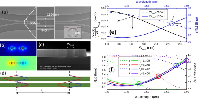
waveguides were proposed in 2004 [87] by using two narrow rails to guide the light, as shown in Figure.1.10. By properly choosing the rail width (Wrail) and slot width (Wslot), a fundamental TE mode
could be formed as in Figure.1.10.a, which shows a strong enhanced electrical field energy in AMs between two rails by about nsi2/nAM2times larger than the field intensity in silicon [87]. AMs suitable for slot waveguides have typically low refractive index values (<1.7) and should be well infiltrated in the nano slots (50nm~200nm).
Figure 1.10 (a) Eelectrical field E of the fundamental TE mode of a typical silicon slot waveguide with a waveguide height h=220nm, rail width Wrail=220nm and slot width Wslot=100nm. The active material was assumed to have the same refractive index as SiO2. The considered wavelength is 1.55µm. (b) An example of fabricated slot waveguides
(in C2N/Orsay, former IEF laboratory, Orsay).
For the widely used SOI waveguides with a silicon height h=220nm, the optical power confinement in single TE mode slot waveguides is around 20% and in the whole low index top cladding around 50%. Such high optical overlap and field energy enhancement (nsi2/nAM2~5) make slot waveguides
very good candidates to study and exploit light matter interactions. For instance, electro-optical slot waveguide modulators embedded with χ(2) have been proved in [88] by using slot TE modes, as shown
in Figure.1.15. Highly nonlinear χ(3) polymers with material Bulk nonlinear FOM up to 5 filled in slot waveguides could result in hybrid slot waveguides with overall waveguide nonlinear FOMwg
=-Re()/4πIm() much larger than those of hybrid silicon strip waveguides [82] ( being the waveguide
nonlinearity coefficient).
Figure 1.11 (a), Schematic picture of a slot waveguide cross-section comprising two silicon rails on a silicon dioxide buffer layer covered by a nonlinear optical organic material, here DDMEBT [82] [80] [79]shown in (b).
1.2.1.2
Further enhancement of light-matter interaction using slow light
waveguides and cavities
Beyond the use of slot waveguides, other physical approaches have also been proposed to enhance hybrid light matter interactions within silicon photonic structures, including slow light photonic crys-tal waveguides [89] and silicon photonic nano cavities [90].
Figure 1.12 Slow light 2D photonics crystal waveguide platform. (left),Slotted photonic crystal waveguides, (right) corrugated and dispersion engineered slot photonic crystal waveguides. [91]
Slow light means light propagating with reduced group velocity vg with respect to the situation in
standard materials. The group velocity vg is given by the dispersion of the wave propagation constant
k (equation 1-8), and usually the group index ng is used as a slowdown factor referring to light
investigated both experimentally and theoretically. For instance, slow waves in photonics could lin-early enhance modal gain 𝑔𝑚𝑜𝑑 = Γ𝐴𝑀
𝑛𝑔
𝑛𝐴𝑀𝑔𝐴𝑀 [92], where gAM is the gain coefficient of the bulk
AMs and nAM is the refractive index of the AM.
𝑣𝑔 = 𝑑𝜔 𝑑𝑘 (1-8) 𝑛𝑔 = 𝑐 𝑣𝑔 (1-9)
Silicon slow light photonic crystal waveguides with group index values typically ranging from 10 to 40 are reasonable, i.e. they can strongly enrich interactions in very short structures while maintaining optical losses at a reasonable level [93]. To achieve desired slow down factors, photonic crystal wave-guides can be dispersion engineered to tune the bandwidth, group index, group velocity dispersion and higher order dispersion terms for controlling light-matter interactions [91], [94]. By chirping the holes size/position, lattice constant, slot size, dispersion engineered slow light slotted photonic crystal waveguides with constant group index band and anomalous dispersion can be achieved (see Fig-ure.1.14) [95]. Ultra-high Q nano cavities with mode volume ~(λ/n)3 have been also achieved in slow light 2D photonic waveguide structures [96]. Photonic crystal cavities with enhancement given by the Purcell factor, were also demonstrated in low index void configurations [97]–[101] The cavity mode confined in the low index region then enables much smaller mode volumes (<(λvac/n)3) than in
standard dielectric cavities. For instance, in [98] as shown in Figure.1.13, an optical mode volume down to 0.0096 (λvac/n)3 and a Q factor up to 150,000 were reported.
Figure 1.13 (Left) Simulated TE mode field distribution of the slotted nanobeam cavities, (Right) fabricated mem-brane slotted nanobeam cavities.
Sandwiched silicon devices as shown in figure 1.14 have also been demonstrated as robust hybrid approaches, in which the functional materials are deposited between two semiconductor layers as an active core layer, requiring at least that the core layers are robust enough and compatible with CMOS
fabrication conditions such as temperature, stress, uniformity of the surface, and etching processes. Typically, simple rib waveguides, one dimensional nanobeam cavities, 2D photonic crystals have been proposed, fabricated and investigated, as shown in Figure.1.14. Lasing was also reported within sandwiched silicon nitride QDs hybrid disks [102].
Figure 1.14 (a) SEM image of an as-fabricated slot wave- guide. a The calculated fundamental TM-like mode profile, b. the plot of normalized electric field along vertical direction at waveguide center and c. AFM image of the fabri-cated slot waveguide. [103]. (b) Scheme of 1D PhC nanocavity on a horizontally SiO2-slotted Si NB [104] (c)
Sche-matics of an active membrane exposed to a focused pump beam (green) and the fibre collecting light from the taper. [92]
Hybrid silicon photonic applications
Due to the broad and rich set of reported works, an exhaustive overview of hybrid silicon photonic applications is difficult. We will mainly focus hereafter on three topics related to applications in op-toelectronic devices, optical amplification/lasing, and on-chip index sensing.
1.2.2.1
Hybrid silicon optoelectronic devices
The typical and widely demonstrated hybrid silicon optoelectronic devices are electro-optical modu-lators relying on the integration of materials such as nonlinear χ(2) polymers , graphene [51] or carbon nanotubes in silicon waveguides [67] [47], [48].
Hybrid silicon organic hybrid (SOH) modulators operating at 100GHz with 3dB bandwidth have been demonstrated in [76]. The EO polymer cladding was coated on top of the silicon slot waveguides and two shallow etched silicon rails were connected with electrodes with reduced resistance by an addi-tional direct voltage, as shown in Figure.1.17.c. This kind of devices was expected to work with on-off-keying data rates up to 140Gbit/s and with voltage-length product as low as VπL=11Vmm.
To reach more compact, lower voltage-length product efficient hybrid modulators, slotted slow light photonic crystal waveguide active devices have been demonstrated. The hybrid integration scheme
of such silicon organic modulator based slow light waveguides is shown in Figure 1.16 [105]. This ref reported a voltage–length product modulating device with a VπL factor of only 0.29 V.mm..
Figure 1.15 Schematic of a Silicon-organic hybrid modulator. (a) The silicon slot waveguide is connected to the metal electrodes by thin silicon strip-loads. The EO polymer cladding covers the waveguide and fills the slot. The shallowly doped silicon substrate is used as a gate. (b) The cross-section of the waveguide and the electric field distribution of the optical quasi-TE mode, where the light is concentrated in the slot. (c) When a positive gate voltage is applied across the 2-mm thick SiO2substrate, a highly conductive electron accumulation layer is formed
in the strip-loads.
Figure 1.16 Scanning electron microscopy (SEM) images of a fabricated device. (a) Tiled view of a local area of the silicon slot PCW modulator. (b) Top view of the slot PCW area. (c) Cross sectional view of the EO polymer refilled silicon slot PCW. PCs, photonic crystals. (d) Zoom-in image of the dashed square area in (c) [105].
Graphene hybrid silicon modulators based on electrically tuned Fermi level of the graphene sheet enabled modulation of the guided light in silicon with frequency over 1GHz [51]. Figure.1.17 shows a schematic view of the graphene layer deposition on top of a silicon waveguide and the presence of Au electrodes. By using ring resonators and detuning the critical coupling extinction ratio, hybrid
graphene modulators could operate with modulation efficiency of 15dB per 10V and at 30 GHz band-width [106].
Figure 1.17 (a) Three-dimensional schematic illustration of a device based on a graphene sheet placed on top of a silicon bus waveguide, separated from it by a 7-nm-thick Al2O3 layer (not shown). (b) Left, cross-section of the
device, with an overlay of the optical mode plot, calculated by finite element simulation. (c,d) Top view of the whole device [51].
To quote few results from the rich literature, graphene and carbon nanotube based photodetectors have also been broadly demonstrated. Typically, graphene photodetectors, as shown in Figure.1.20, could operate from O band to U band at a multigigahertz frequency, with extremely high carrier mobility 200,000cm2V-1s-1 at room temperature and low power consumption 0.5 fJ/bit [47].
Figure 1.18 Waveguide-integrated graphene photodetector. a, Colored scanning electron micrograph of a wave-guide-integrated graphene photodetector. The ‘active region’ of the graphene sheet is shown in purple. The inset shows a cross-section of the device. The graphene sheet coats both the top surface and sidewalls of the waveguide. b, Enlarged view of the section highlighted by the black dashed rectangle in a. The PC flows from the central elec-trode S towards the GND elecelec-trodes. c, Schematic illustration of the band diagram. The dotted line represents the Fermi level, EF. PC is generated in the vicinity of S.WG, waveguide [47].
1.2.2.2
Hybrid silicon optical amplifiers and lasers
As previously mentioned, silicon is an indirect bandgap material and hardly suitable for on-chip las-ing. Table.1.3 reports some of the possible approaches that have been investigated in recent years.
Table 1.3 Silicon light sources: strengths and challenges of the reported solutions; data partly based on [107].
Candidates Er-related light source Ge-on-Si laser III-V based laser Carbon nanotubes
Mechanism Er3+ as emitting source Via bandgap engineer-ing
III-V direct bandgap material as gain
me-dium
Semiconductor nanotubes
Materials SiOx:Er, SiNx:Er, Er
sili-cates, Al2O3 : Er Ge, GeSn alloy
InAlGaAs QW ; InGaAsP QW ; InAs/GaAs QD Semiconductor nanotubes with Emission at 1.2-1.6µm
Advantage CMOS compatible,
wave-length stability
CMOS compatible, large gain spectrum
High gain and output power, commercial
product existed
Both for electronics and photonics Challenge Low electroluminescence,
la-ger net gain per length
Ge materials, ultrahigh threshold current
Reduction of the cost and integration
com-plexity
Nanotube alignment, high concentration integration, obtain gain and lasing. The first promising approach to reach hybrid silicon lasers is to integrate Erbium-doped active mate-rials (AM) on silicon [108]. Erbium, which was demonstrated as an efficient amplifier/laser source in fiber optics, has attracted huge efforts for the realization of on-chip light/amplifiers sources for telecommunications. However, only few devices have been demonstrated with net gain within this approach. Indeed, low loss waveguides and high quality Erbium doped host materials are required for an efficient integration in Silicon. For instance, erbium doped Al2O3 waveguides [109]–[111], Erbium-doped phosphate glass waveguide [112], erbium silicate [113], organo-erbium [74] have been demonstrated with net gain values of around ~1dB/cm to 100dB/cm. However, none of them directly demonstrated such results on silicon photonic waveguides with a net gain of at least on the level ~1dB/mm. The most promising Si-hybrid approach demonstrated in recent years was a silicon (core)/Erbium silicate (shell) nanowire, as shown in Figure.1.20. The crystalline Er silicate corre-sponds to the cladding of the silicon waveguides and provides gain when light propagates along the nanowire, which typically sustains optical modes that are partially confined in Er silicates, as illus-trated in Figure.1.19. This submicrometer optical core (Si) shell (erbium-ytterbium silicate) nanowire, which behaved as an amplifier (see figure.1.19 and 1.20), was demonstrated with a relative gain up to 120dB/mm, but if suffering total loss 210dB/mm, which is possible reduced when nanowire is suspended. However, nanowires are not directly suitable for integrated silicon photonics. Further demonstrations in lithographically fabricated silicon waveguides with a coated erbium silicate clad-ding would be required in order to confirm that transforming core-shell nanowires to a cladded-Si-waveguides could conserve such high gain stability properties within the silicon platform.
Figure 1.19 (a) Schematic of the core-shell nano- structure. (d) (e), optical electrical-field distribution images for HE11 mode with core diameters of 300 nm, 400 nm [114].
Figure 1.20 Microstructure characterization of the Si-EYS core-shell nanowires. (a) Typical SEM images of part of a single nanowire, and (b) its locally amplified image. (c) Cross- sectional TEM image of the wire, and its corre-sponding two- dimensional element mapping (d)–(g). (h) Typical HRTEM image collected at the core-shell inter-face of the wire [red rectangle area in (c)] [114].
Another step showing possible progress towards lasing in hybrid silicon waveguides was provided by the following example. In this hybrid work, a commercial dye-doped organic cladding material, about 500nm thick, was coated on top of 4.8mm-long silicon strip and slot waveguides [115]. As shown in Figure.1.21, Bragg reflectors assisted silicon waveguides coated with an organic cladding were considered.
Figure 1.21 Silicon organic hybrid laser concept. (a) Light is guided by SOI strip or slot waveguides consisting of thin silicon nanowires (width wstrip≈150–500nm, height hWG≈200–350nm). Optical gain is provided by a
fluores-cent organic cladding material (thickness hclad≈500±50nm). (b) Dominant electric field component (Ex) of the
fun-damental TE mode for a narrow strip. (c) Dominant electric field component (Ex) of the funfun-damental quasi-TE mode for a slot waveguide [81].
To reach lasing with nanomaterials, hybrid silicon laser sources with carbon nanotubes have also been proposed. So far, optical gain properties of carbon nanotubes have been demonstrated with CNTs operating at room temperature [66] in pulsed pump regimes within a strip waveguide coated with a-CNT-doped organic layer [116]. In order to reach lasing, CNT interaction in ring resona-tors[117] and nanocavities [65], [118] have been investigated for possible silicon integrated light sources, as shown in Figure.1.23 and Figure.1.24, respectively. Fully integrated carbon-nanotube sil-icon ring resonators are capable of reaching light emission, as shown in Figure.1.24, but still not in the lasing mode. The optical net gain inside the ring resonator was indeed still not sufficient to com-pensate for optical losses in this work. Several recent works have yet shown that integrating carbon nanotubes into silicon photonic nanocavities could potentially enable on-chip lasing [118] [65] by benefiting from high Q and small mode volume effects. At the present time, hybrid carbon nanotube lasing in silicon cavity/resonator is still required to be demonstrated.
Figure 1.22 Integrated carbon nanotube (8,7) silicon ring resonator. (a) Photoluminescence coupled to silicon bus waveguides from the ring resonators, was collected from the end of the silicon bus facet by single mode fiber. (b) silicon ring mode ring resonator with diameter of 10µm and coupled with bus waveguides; HSQ was used to pro-tect the access waveguides (yellow part); single wall nanotube bundles in PFO were spin coated on top of ring resonators in order to have a homogeneous layer as top cladding. The ring resonator was pumped with continuous a laser perpendicularly to the device plane on top [117].
Figure 1.23| An individual carbon nanotube coupled to a nanobeam cavity. (a) A schematic of a device. (b) Scanning electron microscope image of a device with a suspended nanotube. Scale bar is 2 mm. (c) Typical PL spectrum of an air-mode device coupled to a nanotube. The dots are data and the lines are Lorentzian fits. (d) PL excitation map of the device shown in c taken with P¼ 10mWand the laser polarization perpendicular to the nanobeam [118].
1.2.2.3
Hybrid bio-photonic sensing
Hybrid silicon photonic waveguides and resonators described in previous sections also represent an opportunity for other kinds of applications than optical interconnects, among those on-chip sensing is the main one. Bio-detection implemented with microfluidic channels assembled by Lab-On-Chip technologies is required for future healthcare diagnostics[119], [120]. In this perspective, silicon pho-tonics enabling large-scale fabrication of compact planar sensors by integrated CMOS processes is seen as a viable route for massive on chip bio-detection.
Hybrid bio-photonic sensing relies on the functionalizing of the surface of hollow core waveguide resonators/nanocavities with antibodies or other probes, and on the detection of special antibodies binding with antigens by monitoring the resonance shift induced by the bio-chemical reaction, as shown in Figure.1.25 and Figure.1.26. Besides, homogeneous sensing (Sh) is also used to detect gases
[121].
Figure 1.24 Slot waveguides ring resonators with surface treatment of a biotinylated layer in order to bind with avidin-molecules. As slot waveguides have very strong light-matter interaction ability due to enhanced electric field in slot, they have been demonstrated with large waveguide sensitivities according to cladding index changes [122].
Figure 1.25 (a) 3D rendering of the nanoscale optofluidic sensor array device showing two 1-D photonic crystal resonators evanescently coupled to a silicon bus waveguide. The first resonator is immobilized with an antigen whereas the second resonator acts as a control. (b) 3D rendering illustrating the association of the corresponding antibody to the antigen immobilized resonator (not drawn to scale) [123].
Ring resonators and nanocavities have been thoroughly investigated to minimize the so-called sens-ing limit of detection, i.e. the minimum detectable information. Generally, the monitorsens-ing accuracy is qualified in terms of sensitivity and limit of the detections (LOD) of the detection system. In this context, recently developed silicon on insulator (SOI) optical devices have displayed detection ability with LOD down to 10-8RIU and sensitivities exceeding 103µm/RIU by using Vernier effects [124]– [127]. Versatile structures, like single ring resonators (RR) [122], [128], [129], Vernier ring resona-tors [127], photonic crystals (PhC) [99], [130], [131], Mach-Zehnder interferometers (MZI) [126], [132] and Bragg gratings [133] have been demonstrated as highly efficient sensors by the detection of refraction index (RI) changes from the surrounding fluidic channels [120].
Conclusion
Hybrid silicon photonics has been discussed in this chapter, from the material level to the material-waveguide integration and device function ones. Though on-chip lasing through III-V on Si hetero-integration approach has been demonstrated for years as the most successful solution to overcome silicon incapability of light emission, new solutions for silicon light sources still deserve special in-vestigation within silicon hybrid photonic waveguides for further progress, better integration capa-bility, and cost reduction. New demonstrations of silicon hybrid integration with erbium doped ox-ides, graphene, carbon nanotubes, highly nonlinear polymers, lasing dyes, quantum dots are thus wel-come for the realization of on-chip lasers sources and amplifiers. At the present stage of progress, no hybrid integration approach has definitely emerged, so that further investigations are necessary.
Motivations and contexts of the thesis
In this context, the motivations of this thesis are: (1) Exploring how properly integrating Er-doped
materials, semiconductor single wall carbon nanotubes into silicon photonic waveguides; (2) Demon-strating possible hybrid waveguide approaches that could constitute milestones towards integrated optical amplifiers and lasers; (3) Investing the performances of silicon hollow core waveguides for optical index sensing.
The remaining of the manuscript is organized as follows.
Chapter 2 focuses on the design, fabrication and characterization of silicon photonic passive devices including slot waveguides, micro resonators and nanobeam cavities. Optimization of slot waveguides for low losses and high Q factors will be discussed. New types of air mode cavities with high Q and
low mode volumes will be introduced in order to maximize light-matter interaction and improve the stability of the hybrid modes and resonances.
Chapter 3 is dedicated to the integration of Erbium doped PMMA and Er2O3-Al2O3 layers into hollow core Si waveguides for light amplification at =1.55µm. Both numerical and experimental studies will be reported.
In chapter 4, we study the integration of carbon nanotubes with Si waveguide ring resonators and nanobeam cavities in the purpose of optical gain and lasing (yet not fully achieved).
Then, chapter 5 summarizes the main results of this thesis regarding the state of the art. Some limita-tions of the carried out experiments will be mentioned in comparison with new strategies for next steps improvements. The perspectives for silicon amplifiers and hybrid Er-doped polymers and CNTs lasers will then be discussed.
Design and fabrication of passive silicon
photonic structures
Silicon photonic rib and strip waveguides
The basic components of photonic integrated circuits (PIC) are photonic waveguides that are used to draw communications between different blocks by light propagation. When the technologies used to develop PICs are constrained under CMOS fabrication processes, waveguides are formed by lithog-raphy & etching that usually keep rectangular shape cross-sections, as shown in Figure 2.1. The etched sidewalls contribute as the main source of waveguide scattering losses [40][38]. These losses can be reduced by engineering the waveguides cross-section profiles either by considering large width strip waveguides[40] or Rib waveguides [42] (as shown in Figure 2.1.b) to make the electric field intensity interaction with sidewalls decrease. Another option is to increase/decrease (with respect to the mode polarization) the waveguide aspect ratio to push the mode in the low index BOX or cladding layers [38]. Benefiting from advanced 300-mm wafer scale processing techniques [42] for silicon photonic device fabrication, record low loss waveguides (Table.2.1) have been demonstrated in stand-ard waveguides, slot waveguides [134], and grating couplers.
Table 2.1 Present optical loss levels of strip and rib SOI waveguides
Waveguides Type Rib (dB/cm) Strip(dB/cm)
300mm CMOS-platform 0.12±0.01[42] 0.45±0.12dB/cm [134]
Multimode waveguides 0.026 [40]
For silicon platform with 220nm thick silicon film and a 2µm BOX, fully etched silicon strip wave-guides in TM polarization are usually preferred to study the hybridization with cladding active mate-rials (AM), as shown in Figure.2.2. Figure.2.3 quantitatively shows that TM modes in strip wave-guides have indeed typically ~35% of light power confined in the top cladding material while for TE modes this confinement is only about 15% for single mode situations.
Figure 2.1 Schematic pictures of: (a) Rib waveguides, (b) Strip waveguides. Waveguide modes are shown at =1.55µm for a TE-like polarization in (c) and (d).
Figure 2.2 Cross-sectional view of power confinement of typical SOI strip waveguides at =1.55µm: (a) TE polarization; (b) TM polarization.
Figure 2.3 Total Power confinement in top cladding for strip SOI waveguides (hSi=220nm) in TE and TM polariza-tions as a function of the waveguide width (=1.55µm).
350 400 450 500 550 10 15 20 25 30 35 40 45 50 P_cladd ing (%) Wstrip (nm) TE-P_cladding TM-P_cladding Strip Wg
Slot waveguides
In view of the limited amount of optical power interacting with surrounding materials in Si strip waveguides, hollow waveguides entitled slot waveguides have been proposed for years [135]. We report in this part our contribution to the design, fabrication, and characterization of such silicon and silicon nitride slot waveguides for the hybrid integration of soft materials and liquids on silicon.
Silicon slot waveguides
2.2.1.1
Silicon slot waveguides modes and energy confinement
As stated in chapter 1, slot waveguides with TE modes (Figure2.4.a) not only partially confine light in the void low refractive index (RI) regions but are also responsible for a field reinforcement in the slot by a ratio of 𝑛𝑆𝑖2/𝑛𝑐𝑙𝑎𝑑𝑑2 . An interesting metrics of these waveguides in Si photonics is the optical power confinement in the tiny slot, which is about 22% for different slot widths for TE modes (Fig-ure2.5), while for TM modes (Figure2.4.b) light confinement maximum value is about 10%. However, the whole power confinement in the top low RI cladding material for both polarizations is above 40% with a 5-8% higher level for TE than for TM modes (Figure2.5). To conclude, both of the two polar-ized modes have a large power overlap with the top cladding material in slotted waveguides. TE modes are yet much better suited than TM ones for light-matter interaction considering much strong electric field enhancement in the slot region and a bit higher power confinement in the total cladding region.
Figure 2.4 Cross-sectional view of total power confinement of typical SOI slot waveguides for TM and TE light polarizations. (a) TE and (b) TM at =1.55µm.
Figure 2.5 Total power confinement in slot region only and whole cladding (including slot) of slot SOI waveguides as a function of the slot width and for TM and TE polarization of light (=1.55µm).
Optimization of light confinement in the top cladding region for TE modes can be investigated by considering wide ranges of slot and rail widths, as shown in inset of Figure.2.6.b, which gives an example [136] considering a highly nonlinear χ(3)top cladding polymer with refractive index 1.8. It can be seen, as a general trend, that when the rail width becomes smaller and the slot width increases, light confinement in the slot region increases. Typically, maximum confinement power levels around 75% are possible for silicon slot waveguides. For real device design, the whole set of parameters, including the slot and rail widths should be globally considered. For instance, optimization of non-linear FOM should be considered [136] for nonnon-linear hybridization, waveguide sensitivity needs to be maximized for optical sensing [137], and propagation losses should be reduced for optical ampli-fication or lasing. With the development of the etching processes, silicon slot waveguide losses have been now reduced down to 2dB/cm in present state of the art works [134].
Figure 2.6 Optical power confinement in silicon rails (Si), top cladding (CC) and above BOX (CC+Si); (a) when con-sidering slot width =100nm; (b) when concon-sidering rail widths of 170nm width (=1.55µm). The top cladding is envisioned as nonlinear polymer DDMEBT with refractive index 1.8.
40 60 80 100 120 140 160 180 200 220 10 20 30 40 50 Stlot Wg Power Conf inem en t ( %) Wslot (nm) TE-P_slot TE-P_cladding TM-P_cladding TM-P_slot (a) (b)
2.2.1.2
Silicon slot waveguides fabrication
2.2.1.2.1 Fabrication challenges
Fabrication challenges of slot waveguides mainly include two parts: mode converters and low loss long slot waveguides. Mode converters are usually used to properly connect strip and slot waveguides with the purpose of reducing back reflections while reaching high transmission efficiencies. Long (>>100µm) slot waveguides fabrication under e-beam lithography face e-beam current instabilities during long and large scale path writings, which also inevitably induce stitching errors, slot width variations along the whole waveguide and thus larger propagation losses.
2.2.1.2.1.1 Slot mode convertors
A slot waveguide mode converter, which transforms a strip mode to a slot mode, can be realized through symmetric multimode interferences [138], Y-branch couplers [139], “tip insertion” [140] and logarithmic side tapers [141]. All these kinds of couplers can reach coupling efficiencies more than 90% and logarithmic side tapers could reach the best efficiency of 99.5% with logarithmically tapered width [141]. However, all the mode converters face the problems of the conversion efficiency when slot size goes down to 100nm considering the larger scattering losses in tiny slots and minimum lithography exposure/etching feature sizes. Besides, the designed mode converters are not universal for all different slot and rail width configurations.
The minimum slot feature size in our clean room fabrication is around 40nm. The slot feature size in our .gds-II file is 20nm in order to well isolate silicon to form a minimum slot ~40nm, as shown in Figure.2.7 and Figure.2.8. Figure.2.7 shows an example of “tip insertion” mode convertor fabrication, where slot size at beginning was set with 20nm and ends with 10nm in the .gds-II file (shown in Figure.2.7.a). Figure.2.7.c shows that the slot nearly vanishes when the .gds-II slot dimension is re-duced to 10nm and indeed, Figure.2.7.b proves that the slot was not successfully formed for the 10nm .gds-II value.
Figure 2.7 “Tip insertion” slot mode converters. (a) Insertion slot size from bottom to top was modulated from 20nm to 10nm in .gds-II files; (b) The top tip slots was not isolated due to a too small exposure; (c) The bottom slot was, on the contrary, well isolated.
(c)
A good control of the this “tip insertion” mode convertor is obtained by reducing the .gds-II slot dimension from 20nm to 15nm, which finally contributes to a proper isolation of the silicon rails, as illustrated in Figure.2.8. The present whole mode convertor length is 20µm and the two side slot widths are around 50±10nm from beginning to end, as measured in Figure.2.8.
Figure 2.8 Tip insertion slot mode converters. (a) Cross-section of the beginning part of the taper; (b) SEM global view of the well fabricated taper; (c) Cross-section of the end of the taper.
A second type of “side” mode convertor [142] was also fabricated by following ref [142], which rigorously explains that logarithmically tapering the waveguides width would optimize the transmis-sion efficiency as displayed in Figure.2.9. The strip waveguide initially that sustains a single mode (Figure.2.9.a) begins to evanescently excite the slot waveguide field due to its narrowing width and ultimately a true slot mode as plotted in Figure.2.9.c. Let notice that this design is made of only one slot width, which is of a larger width than the ones used in the “tip insertion” mode convertor config-uration, which eases the slot fabrication. In this second convertor type, a side rail follows the strip waveguide with a constant slot width until the strip width (linearly or logarithmically) reducing down to the same width as the side rail. Figure.2.10.b shows one fabricated “side” mode convertor with a slot width of 95nm and a rail width of 220nm by linearly tapering the strip waveguide width down to 220nm. Logarithmically tapering methods were not adopted by us considering that a linear tapering was enough with respect to fabrication uncertainties in the design of a logarithmic profile. Experi-mentally, we characterized the losses per “side” mode converter to around 0.07dB for different slot widths, as summarized in Table.2.2, which is a bit larger than the state of the art of 0.02dB for the logarithmically tapered ones but yet fairly acceptable. “Tip insertion” slot mode converters proved to have transmission losses around 0.25dB, ie 3 times larger than “side” converters. Sometimes, fabri-cation instabilities could also enlarge conversion losses several times higher, for instance, 1.2dB for “tip insertion” converter with slot width 110nm and 0.21dB for “side” converter with 130nm slot width.
Figure 2.9 Mode transitions along the “side” mode converter from (a) strip waveguide mode to (c) slot waveguide mode. The whole transitions process are depicted in (c) [142].
Figure 2.10 “Side”-type slot mode converters. (a) Cross-section of the beginning part of the taper; (b) SEM over-view of the well fabricated taper; (c) Cross-section of the end of the taper.
Table 2.2 Summarized losses per mode converters with different slot widths at the wavelength of 1.55µm.
Slot width 90nm 110nm 130nm 150nm
“Tip” 0.26dB 1.2dB 0.67dB 0.25dB
“Side” 0.088dB 0.074dB 0.21dB 0.059dB
To conclude this part, the design method of “side” mode convectors is simple and their fabrication was verified as very robust compared with “tip insertion” convertors. The reasons for this stem in several points: i) Lateral tapers do not require tiny slots as “tip convertors” do , thus inducing less fabrication errors; ii) They suffer lower light back reflection levels. This is the reason why lateral strip to slot convertors have been preferred and considered for most of the realizations presented in this manuscript.
2.2.1.2.1.2 Stitching errors in slot waveguides
Stitching errors, the deviation from perfect alignment between consecutive writing subfields or main fields, have been found more frequently in fabricated slot waveguides than in strip ones, especially inside bended slot waveguides between two consecutive writing subfields, as shown in Figure.2.11.a. The realization of slot ring resonators with a diameter of 100µm, for example, requires an e-beam exposure in 58 subfields (10µm×10µm) during the e-beam lithography writing process. This long curved slot waveguide path needs to be cut into different small polygons in each subfield. In some subfields, the polygons are so small that stitching errors occur when the gds-II files are interpreted

![Table 1.3 Silicon light sources: strengths and challenges of the reported solutions; data partly based on [107]](https://thumb-eu.123doks.com/thumbv2/123doknet/14529139.723300/25.892.82.838.273.483/table-silicon-sources-strengths-challenges-reported-solutions-partly.webp)