HAL Id: hal-02998364
https://hal-amu.archives-ouvertes.fr/hal-02998364
Submitted on 11 Nov 2020HAL is a multi-disciplinary open access archive for the deposit and dissemination of sci-entific research documents, whether they are pub-lished or not. The documents may come from teaching and research institutions in France or abroad, or from public or private research centers.
L’archive ouverte pluridisciplinaire HAL, est destinée au dépôt et à la diffusion de documents scientifiques de niveau recherche, publiés ou non, émanant des établissements d’enseignement et de recherche français ou étrangers, des laboratoires publics ou privés.
Distributed under a Creative Commons Attribution| 4.0 International License
Interactions between Terrestrial Cosmic-Ray Neutrons
and III-V Compound Semiconductors
Daniela Munteanu, Jean-Luc Autran
To cite this version:
Daniela Munteanu, Jean-Luc Autran. Interactions between Terrestrial Cosmic-Ray Neutrons and III-V Compound Semiconductors. Modeling and Simulation in Engineering, 2020, 978-953-51-0012-6. �10.5772/intechopen.92774�. �hal-02998364�
Interactions between Terrestrial
Cosmic-Ray Neutrons and III-V
Compound Semiconductors
Daniela Munteanu, Jean-Luc Autran Aix-Marseille University, CNRS, University of Toulon, IM2NP, UMR 7334, Faculté des Sciences, F-13397 Marseille Cedex 20, France [email protected] Abstract This work explores by numerical simulation the impact of high energy atmospheric neutrons and their interactions with III-V binary compound semiconductors. The efforts have focused on eight III-V semiconductors: GaAs, AlAs, InP, InAs, GaSb, InSb, GaN and GaP. For each material, extensive Geant4 numerical simulations have been performed considering a bulk target exposed to a neutron source emulating the atmospheric neutron spectrum at terrestrial level. Results emphasize in detail the reaction rates per type of reaction (elastic, inelastic, nonelastic) and offer a classification of all the neutron-induced secondary products as a function of their atomic number, kinetic energy, initial stopping power and range. Implications for single event effects are analyzed and discussed, notably in terms of energy and charge deposited in the bulk material and in the first nanometers of particle range with respect to the critical charge for modern CMOS technologies.
Keywords: radiation effects, III-V compound semiconductors, cosmic-rays,
atmospheric neutrons, numerical simulation, neutron cross section, elastic scattering, inelastic scattering, nonelastic interactions, nuclear data library, Geant4.
1. Introduction
The introduction of III-V high-mobility semiconductor materials into advanced CMOS manufacturing is currently envisaged as a possible “technological booster” for carrier mobility enhancement. Indeed, for nanometer-scale transistor, it will not be possible to maintain the power–performance tradeoff offered by conventional silicon-based technologies because of the transport properties of Si that are becoming a fundamental limitation for ultimate CMOS [1-2]. Several materials exhibiting higher carrier mobilities than Si are currently exploring for both n-channel and p-channel transistors. Between all these materials, GaAs, InAs, InGaAs and InP are suitable candidates for n-channel devices and GaSb and InGaSb for p-channel transistors [3-5].
In complement to their physical and electrical characterization, the exploration of the radiation response of these III-V materials is also an important concern for predicting their reliability. Several studies investigating total ionizing dose (TID),
heavy ion and laser responses of III-V MOS transistors in modern architectures, as well as the creation mechanisms of single event effects, have been reported in literature but relatively little work concerns their response to terrestrial neutrons [6-13]. In two recent papers [14-15], we begun such a systematic investigation of the susceptibility to natural radiation of group-IV and III-V materials exposed.
The aim of this chapter is to provide new data and metrics for this exploration via Geant4 [16-17] numerical simulations of the radiation response of III-V binary compound semiconductors subjected to high energy atmospheric neutrons. The study specifically focuses on eight III-V materials: GaAs, AlAs, InP, InAs, GaSb, InSb, GaN and GaP. For each material, the reaction rates for elastic, inelastic and nonelastic events have been determined as well as the classification of all produced secondaries as a function of their atomic number, kinetic energy, initial stopping power and range in the target bulk. Average energy and charge deposited in the bulk material and in the first nanometers of particle ranges have been also evaluated. These later quantities are important statistical metrics in the occurrence of single event effects (SEE [18]); they have been compared with the critical charge for various CMOS technologies (180nm to 14nm nodes).
The chapter is organized as follows. Section 2 presents the different compound materials studied and summarizes their main physical and electronic properties. Section 3 details the Geant4 numerical simulations conducted in the framework of this study. Section 4 presents the complete analysis of interactions databases in which all neutron-induced secondaries have been recorded for each material subjected to atmospheric neutrons. Finally, in section 5, implications for single event effects in CMOS based on these semiconductor materials are analyzed.
2. Semiconductor properties
III-V binary compound materials explored in this work are semiconductor alloys containing one element from group III (boron column: Al, Ga, In) and one from group V (nitrogen column: N, As, Sb) of the periodic table. Table I shows the natural isotopic abundance for these six chemical elements. For example, natural gallium (31Ga)
consists of a mixture of two stable isotopes: 31-Ga-31 at 60.10% and 31-Ga-71 at 39.90%. Numerical simulations presented in the following take into account such isotopic compositions for each element present in the eight studied materials.
Symbol number Atomic Nuclide abundance Natural
Al 13 13-Al-27 100.00%
Ga 31 31-Ga-69 31-Ga-71 60.10% 39.90%
In 49 49-In-115 95.70% 49-In-113 4.30% N 7 7-N-14 7-N-15 99.60% 0.40% P 15 15-P-31 100.00% As 33 33-As-75 100.00% Sb 51 51-Sb-121 57.40% 51-Sb-123 42.60% Table 1. Natural abundance of nuclides related to the III-V alloys studied in this work.
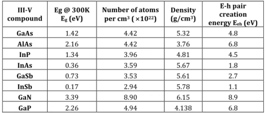
III-V compound Eg @ 300K Eg (eV) Number of atoms per cm3 ( ´1022) Density (g/cm3) E-h pair creation energy Eeh (eV) GaAs 1.42 4.42 5.32 4.8 AlAs 2.16 4.42 3.76 6.8 InP 1.34 3.96 4.81 4.5 InAs 0.36 3.59 5.67 1.8 GaSb 0.73 3.53 5.61 2.7 InSb 0.17 2.94 5.78 1.1 GaN 3.39 8.90 6.15 8.9 GaP 2.26 4.94 4.138 6.8 Table 2. Main properties of the III-V binary semiconductors considered in this study. Partially from [19]. Table 2 summarizes the main experimental values for GaAs, AlAs, InP, InAs, GaSb, InSb, GaN and GaP bulk materials in terms of energy bandgap Eg, number of atoms per volume unit, density [19], and electron-hole pair creation energy Eeh. All these crystalline solids are denser than Si (2.32 g/cm3). The following materials, GaAs, AlAs, InP, GaN, GaP, are characterized by a bandgap larger than Si and, consequently, by a larger electron-hole pair creation energy (3.6 eV for Si). The other materials, i.e. InAs, GaSb, InSb, have a bandgap clearly below 1eV; Eeh values for these materials are also lower than the one of Si. Finally, for GaSb and InSb, we did not find in literature an experimental value for Eeh; we used by default the values deduced from the Klein’s
model [20] establishing a linear relationship between Eg and Eeh in semiconductor
materials.
3. Geant4 numerical simulations
Geant4 simulations were carried out following a methodology used in previous works [14,21-22]. We considered a target of bulk material (composed of a pure material chosen between the eight binary compounds studied) with a parallelepiped geometry (surface 1 cm2, thickness 20 µm). Each target was virtually irradiated with
neutrons arriving perpendicularly to the surface and for which the energy distribution follows the terrestrial natural neutron background at sea level. This latter was chosen equal to the high-energy (above 1 MeV) neutron spectrum measured by Goldhagen et al. at sea level (New York City) [23-24]. A total of 108 of incident neutrons was considered, representing the equivalent duration of 5x10⁶ h of natural neutron irradiation at sea level. Geant4 version 4.9.4 patch 01 was used for these simulations. The list of physical processes employed in these simulations is based on the standard package of physics lists QGSP_BIC_HP [25]. Other simulation details can be found in Ref. [21]. Outputs of each simulation consist in a series of files containing all the information related to the neutron interaction events in the target material. For each event, this information includes the nature and the coordinates of the vertex of the interaction, the energy of the incident neutron, the exhaustive list of secondary particles produced during the interaction, the energy and the emission direction vector for each of these emitted particles. All these records have been post-treated and formatted into the final interaction databases (text files) following two compilation rules: i) we eliminated in the output file (raw data) all secondaries below 1 keV of energy; ii) we also eliminated all g photons, p0, e+, e- and h particles, these particles being not able to deposit 1 keV
of energy in the targets, which is a mandatory condition to observe single event effects in electronics. The computational time was approximately of three weeks for
eight parallel runs on multi-core 3 GHz CPUs; the code being executed on separate cores for each material. 4. Simulation results Table 3 gives the distributions of elastic, inelastic and nonelastic events recorded in the different III-V compound material databases. Values for the database related to silicon are also reported for comparison. For memory, the interactions of neutrons with atomic nuclei can occur through two major mechanisms: scattering (which can be subdivided in elastic and inelastic processes) and capture (also called non-elastic) [26]. When a neutron is involved in an elastic scattering, the nature of the interacting particles is not modified; in particular the recoil nucleus is then the same as the target nuclei A or B in the case of a binary compound material AB. Similarly, during an inelastic scattering, the impacted target nucleus A or B undergoes an internal rearrangement into an excited state from which eventually releases radiation. Instead of being scattered, an incident neutron may be absorbed or captured by a target material nucleus A or B. Many reactions are possible, and a large variety of particles can be emitted. This type of interaction is also called nonelastic interaction.
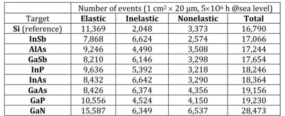
As evidenced by results of Table 3, the eight III-V materials show an interaction rate superior to the value observed for the reference case with Si even if GaSb, AlAs and InSb show a number of interaction events the closest from the one of Si. A single material stands out clearly from the others in terms of very high number of interactions: GaN. This result is the direct consequence of GaN crystallographic structure that leads to a number of atoms per volume unit almost double with respect to all other materials (see Table 1).
Concerning elastic events, their proportion is clearly predominant for Si (68%), GaP, GaN (55%), AlAs (54%) and InP (53%). The sum of inelastic and nonelastic events is above 50% for GaAs (56%), InAs, InSb (54%) and GaSb (53%). For Si, this sum is only around 32%, which is lower than 40% found in previous studies [21]. The reason is that, in the present case, the minimum kinetic energy (energy cutoff) to take into account recoils and secondaries in the databases has been fixed to 1 keV, whereas this value was fixed to a higher value, i.e. 40 keV, in previous studies. According to [15], the number and, consequently, the proportion of elastic events with respect to inelastic and nonelastic events clearly depends on such energy cutoff; it is the reason why these percentages may vary.
Number of events (1 cm2 ´ 20 µm, 5´1O6 h @sea level)
Target Elastic Inelastic Nonelastic Total
Si (reference) 11,369 2,048 3,373 16,790 InSb 7,868 6,624 2,574 17,066 AlAs 9,246 4,490 3,508 17,244 GaSb 8,210 6,146 3,298 17,654 InP 9,636 5,392 3,218 18,246 InAs 8,432 6,642 3,290 18,364 GaAs 8,426 6,374 4,356 19,156 GaP 10,556 4,524 4,150 19,230 GaN 15,587 6,349 6,537 28,473
Table 3. Number of elastic, inelastic and nonelastic interactions induced by
atmospheric neutrons in the different III-V binary compound materials obtained from Geant4 simulations.
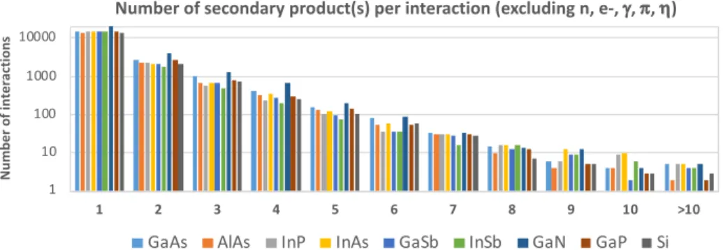
Figure 1. Number of secondary product(s) per interaction (after excluding g photons,
p, e+, e- and h particles as explained in the text).
Figure 2. Number of secondaries in the events recorded in the eight III-V material
databases for the four product classes defined in the text. The nature of recoils is indicated for each material. Results for silicon are also shown for reference.
Figure 1 shows the number n of secondary product(s) per interaction for the different materials. It is important to note that n has been evaluated after excluding g photons, p, e+, e- and h particles from the raw simulation data, as mentioned in Section
3. As a consequence, the first class of the distribution, i.e. n=1, corresponds to single product reactions that only result in a single recoil after interaction. These reactions correspond to all elastic and inelastic events, totalized in Table 1. For n>2, all secondaries are produced during nonelastic interactions, with an average number of secondary products per reaction between 2.5 and 2.7 for the different III-V materials (2.6 for silicon). Note that GaN and, in a lesser extent GaAs and GaP, show the most important number of reactions for n ranging from 2 to 5. To understand these results, a more detailed analysis in terms of secondary products must be conducted. Precisely, Figure 2 shows the distribution of secondaries produced in the different targets of III-V binary compound materials subjected to atmospheric neutrons. Four groups of particles have been defined as a function of the atomic number Z: i) protons, deuterons and tritons (Z=1), ii) alpha particles and He-3 (Z=2), iii) nuclei corresponding to target atoms (named recoils #1 and #2 for binary compounds) and iv) other nuclei (with Z different from the other three categories). 1 10 100 1000 10000 1 2 3 4 5 6 7 8 9 10 >10 Num be r of inte rac tions
Number of secondary product(s) per interaction (excluding n, e-, g, p, h)
GaAs AlAs InP InAs GaSb InSb GaN GaP Si
0 2000 4000 6000 8000 10000 12000 14000 16000
InSb Si GaSb AlAs InP InAs GaP GaAs GaN
Num be r of pr oduc ts
Secondaries produced in all interactions (1cm2x 20 µm, 5x10⁶h @ sea level)
protons, deuterons, tritons alphas, He-3 Recoils #1 Recoils #2 Others
Geant4 databases
Product energy cutoff 1 keV
In Sb Si Ga Sb Al As Ga Ga As Ga N In In P As
Figure 2 shows that similar distributions of these particle groups are found for all materials, GaN excepted, with approximately 20-25% of protons+alphas, 60% of recoil products constituted of target nuclei and the remaining 15% of other nuclei. In the case of GaN, the proportion of protons and alpha particles is more important and correspond to approximately two times the proportion observed in silicon; this result can be explained by the additional production channels of protons and alpha particles offered by the 14N(n,p)14C and 14N(n,a)11B reactions [27]. Always for GaN, the
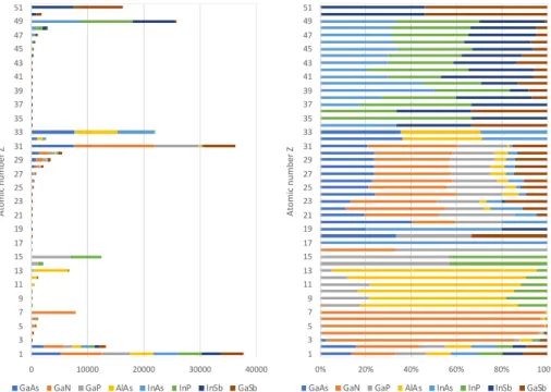
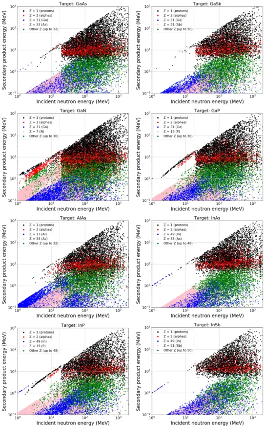
combination of a high number of atoms per volume unit and the presence of nitrogen is at the origin of such a large difference with respect to other III-V materials in terms of a higher number of interactions, of secondaries produced and of alphas and protons. In addition to Figure 2, Figure 3 shows the exhaustive distribution of all secondaries produced in all materials as a function of Z. The stacked declination of the histograms is only to produce a clearer comparison figure; there is of course no physical sense to add secondaries of same Z induced by neutrons in different targets other than specifying their distribution in Z. Figure 4 shows the energy mappings for all secondaries produced by atmospheric neutrons in the eight different targets. In these figures, each colored point correspond to a single secondary product; the x-coordinate of the point corresponds to the energy of the incident neutron which gave birth to it; the y-coordinate corresponds to the kinetic energy of the secondary after its release at the level of the reaction vertex. The same four groups of particles as previously defined (Figure 2) have been considered. Such product energy mappings allow us to visually compare the contain of the different databases and to highlight similarities and differences between the atmospheric neutron susceptibilities of the eight studied materials, notably in terms of protons, alphas (GaN and GaAs as compared to InSb and InP) and recoil distributions (differences between light and heavy recoils: N, Al and P as compared to Ga, As, In and Sb). In Figure 4, we can see that all points are logically below the straight-line y=x because the maximum energy of secondary products is, at most, equal to that of the incident primary neutron. Figure 3. Distribution in number (left) and in percent(right) of all secondaries produced in all materials as a function of their atomic number. 0 10000 20000 30000 40000 1 3 5 7 9 11 13 15 17 19 21 23 25 27 29 31 33 35 37 39 41 43 45 47 49 51 Ato m ic n um be r Z
GaAs GaN GaP AlAs InAs InP InSb GaSb
0% 20% 40% 60% 80% 100% 1 3 5 7 9 11 13 15 17 19 21 23 25 27 29 31 33 35 37 39 41 43 45 47 49 51 Ato m ic n um be r Z
Figure 4. Energy distributions as a function of the incident neutron energy for all
secondaries produced in the events recorded in the eight III-V material databases.
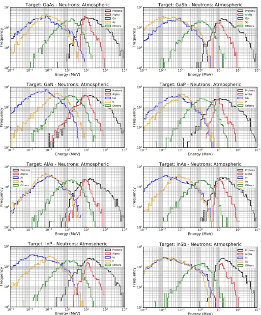
Figure 5. Energy histograms (100 bins) of protons, alphas, target nucleus recoils and
other ions produced by atmospheric neutron interactions in the eight III-V bulk material targets.
From data of Figure 4, we deduced the energy histograms of Figure 5 for all the secondary products in the eight materials. To limit the number of curves, these histograms have been calculated for the four classes of secondaries previously defined, i.e. for protons, alpha particles, target nucleus recoils and other ions. These energy histograms show the same information as in Figure 4 but in a more compact and quantitative form. These curves indicate the energy domain covered for each type of particle and also the energy position of the maximum of the distributions. For recoil products, the heavier the recoil nucleus, the lower the energy of the maximum of the distribution. For protons, alphas and other nuclei, similar distributions and energy domains are obtained (from 10-1 to 103 MeV for protons, from 1 to 102 MeV for alphas,
from 10-2 to a few tens of MeV for other nuclei) for the different targets, excepted for
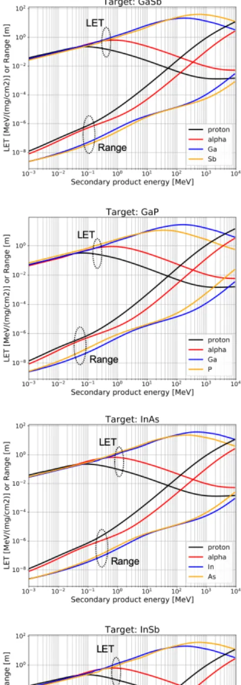
evidenced in the range of 0.1 to 1 MeV; for InAs and InSb, proton distributions are narrower and only cover an energy range between 1 and 103 MeV. Figure 6. Linear energy transfer (LET) and range related to protons, alphas and recoil products in the eight III-V materials calculated with SRIM.
From the above data, we deduced the linear energy transfer (LET) and range distributions of all secondary products for the different target materials. For memory, the linear energy transfer or LET of a charged particle refers to the stopping power, i.e. the energy lost by unit of length, due only to electronic collisions and expressed in MeV/(mg/cm2) or in keV/µm. The range corresponds to the distance that a charged particle travels from its emission point through matter until it comes to rest. Both LET and range primarily depend on the type and initial energy of the particle and of the medium (i.e. the target material) in which the particle travels.
We used the popular and reference code SRIM (Stopping and Range of Ions in Matter [28-29]) to perform (in batch mode controlled from a short C-code) the automatic calculation of the LET and range tables (in the range 1keV to 10 GeV) for all possible nuclides from Z=1 to Z=92, which represents 2,670 SRIM tables per material. A total of 2,670 ´ 8 = 21,360 files were computed and indexed in different folders in order to be directly read from a python code to automatically compute LET and range histograms. Figure 6 shows the plots of SRIM tables for LET and range related to protons, alphas and recoil products in the eight III-V materials.
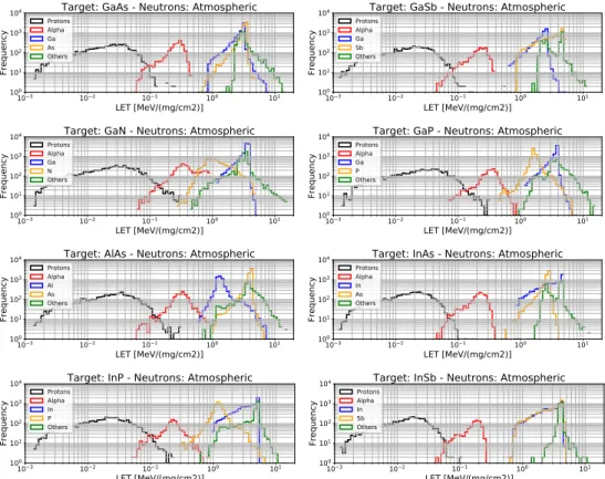
The cross-combination of these SRIM data with particle types and energies listed in the different interaction databases was performed using a dedicated python script to compute (by linear interpolation of the SRIM tables) the initial LET (at product release) and the range histograms of all products, shown in Figures 7 and 8 respectively. Figure 7. Initial LET histograms (100 bins) of protons, alphas, target nucleus recoils and other ions produced by atmospheric neutron interactions in the eight III-V bulk material targets.
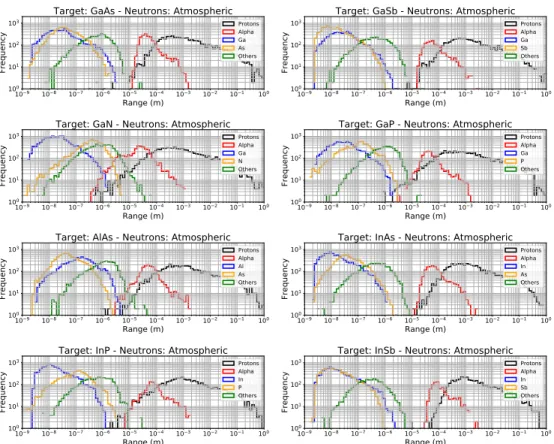
Figure 8. Range histograms (100 bins) of protons, alphas, target nucleus recoils and
other ions produced by atmospheric neutron interactions in the eight III-V bulk material targets.
Figures 7 and 8 logically show that the smaller the particle, the lower the initial LET and the higher the range of the particle. Thereby protons exhibit the lowest LET values, in the interval from 10-3 to a few 10-1 MeV/(mg/cm2) for all materials, and the
highest ranges, typically from 10-6-10-5 m to a few tens of cm. Alphas particles are
characterized by intermediate values, with typical initial LET values between 0.1 to 1 MeV/(mg/cm2) and ranges in the domain from the micron to millimeter. Finally,
recoil products and other nuclei exhibit the highest initial LET values, up to 10 MeV/(mg/cm2) and the lowest ranges, from the nanometer to a maximum of few tens
of microns. These results strongly suggest that products recoils will play and increasing role in submicron and nanowire devices, as explored in the following. 5. Discussion
In complement to [15], we examine, in this last section, some consequences of the above results in terms of creation of single event effects in electronics based on the studied III-V materials. Following neutron interactions with target nuclei and release of secondaries, the energy deposition of these secondary products in the bulk material and its conversion to free charge via the creation of electron-hole pairs is another fundamental step in the creation of SEEs.
First, we evaluated two global metrics to quantify such an energy deposition consecutive to neutron interactions in the bulk of the III-V materials: i) the mean value of deposited energy per interaction (averaged over all events) and ii) the corresponding amount of created electron-hole pairs. These two metrics have been
evaluated, in Figure 9, for the different materials. The first metric, i.e. the mean energy deposited per interaction, is found to vary from around 9 MeV for Si to 14 MeV for GaAs. Atmospheric neutron interactions deposit, in average, more energy in III-V materials than in Si. This result is the consequence of a difference in the number of nonelastic interactions, which is higher in III-V materials than in Si, as shown in the following (Figure 10 and text). Figure 9 compares the number of e-h pairs created per interaction in the different III-V materials with respect to the value obtained for silicon (relative factor). Three groups of materials can be considered: 1) GaAs, AlAs, InP, GaN and GaP that are found very similar to Si (relative factor close to 1 with respect to Si); 2) InAs and GaSb which exhibit a relative factor between 1.5 and 2.5 and, finally, 3) InSb characterized by the highest factor, close to 4. For the first group of materials, the higher atmospheric neutron sensitivity of these materials (which is indicated by the number of interactions) is largely compensated by a higher energy of e-h pair creation at semiconductor level, due to their large bandgap. On the contrary, for the three last materials which are lower bandgap semiconductors (see Table I), their vulnerability to atmospheric neutrons is finally reinforced by their electrical response level due to the relatively low values of the energy of e-h pair creation. Figure 9. Deposited energy per interaction (mean value estimated from all events) and corresponding amounts of e-h pairs created in the different III-V material targets. Values have been evaluated considering for each material the e-h pair creation energy given in Table I. Typical values for silicon are also indicated for reference. Figure 10. Averaged values of the deposited energy per elastic or inelastic interaction and per nonelastic interaction for the different III-V material targets. For the case of elastic or inelastic interactions, values have been multiplied by a factor ´100 to be plotted on the same scale.
Global results of Figure 9, however, do not show important quantitative differences that exist between the respective contributions of, on one hand, elastic or
0.0 5.0 10.0 15.0
GaAs AlAs InP InAs GaSb InSb GaN GaP Si
Ee nr gy (Me V) Num be r of e -h pair s (m illions)
Average energy deposited per interaction Average number of e-h pairs created per interaction
0 10 20 30 40 50 60 70 80
GaAs AlAs InP InAs GaSb InSb GaN GaP Si
Ene
rgy (Me
V)
inelastic interactions and, on the other hand, nonelastic reactions, to these global values. In order to examine this particular point, we recalculated the average energy deposited per interaction. Results are shown in Figure 10. Elastic or inelastic interactions deposit, in average, between 0.1 MeV (GaSb) and 0.25 MeV (GaN) with a value of 0.23 MeV for Si. On the contrary, nonelastic interactions deposit, in average, more than 50 MeV for GaN and up to 75 MeV for InSb, with a comparative value of 45 MeV for Si. In other words, noneleastic interactions deposit approximately between ´200 (GaN) and ´600 times (GaSb) more energy in average than elastic or inelastic events. Because these nonelastic events are less numerous than elastic+inelastic events (see Table 3), this explains why the global average energies per interaction (Figure 9) are relatively modest, distributed between 10 to 15 MeV. But these values hide very different situations, depending on the type of interactions. Converted into electron-hole pairs, nonelastic reactions are able to deposit, in average value integrated over all the secondary tracks, deposited charges up to a few pC whereas elastic or inelastic reactions hardly reach values around a few fC.
In addition to the previous results, we evaluated the fraction of the total energy deposited per type of secondaries for all interaction events in the semiconductor bulks. Results are shown in Figure 11. Surprisingly enough, over 85% of the total energy deposited in the different III-V materials is deposited by protons, followed by alpha particles (around 10%). Other nuclei and recoil products represent less than 5% whereas for silicon, they represent around 8% and alphas only 5%. Considering the range of protons and alphas, this result shows that the largest part of the energy is deposited far from the location of the reaction vertex.
Figure 11. Fraction of the total energy deposited per type of secondaries for all
interaction events in the bulk of the studied III-V semiconductors. Figure 12. Fraction of the total initial LET deposited per type of secondaries for all interaction events in the bulk of the studied III-V semiconductors. 75% 80% 85% 90% 95% 100%
GaAs AlAs InP InAs GaSb InSb GaN GaP Si
Fraction of the total energy deposited per type of secondaries for all interaction events
protons alphas recoils others
0% 20% 40% 60% 80% 100%
GaAs AlAs InP InAs GaSb InSb GaN GaP Si
Fraction of the total initial LET per type of secondaries (averaged over all secondaries for all interaction events)
Conversely, if we consider the fraction of the total initial LET deposited per type of secondaries for all interaction events in the different materials, we obtain results shown in Figure 12. For III-V material, 70% to 80% (minimum for GaP, maximum for InSb) of the total of the initial LET values corresponds to recoil products. The remaining 10% is related to other nuclei, the contributions of protons and alpha particles being negligible in this total initial LET. This signifies that recoil products are essentially at the origin of the charge deposited in the first (tens of) nanometers around the incoming neutron interaction point (also called reaction vertex).
To evaluate the deposited charge in the first nanometers around reaction vertex points, we derived this quantity from the initial LET of particles just after their
release. Introducing Eeh, the energy needed for creating an electron-hole pair given in
Table 2 and tSi the thickness of the material thin layer in which the charge Qdep is
deposited, we obtain [13]:
𝑄!"#[𝑓𝐶] = 𝐴´LET[𝑀𝑒𝑉/(𝑚𝑔/𝑐𝑚2)] ´ tSi[µ𝑚] (1)
where A is a numerical factor that only depends on the semiconductor material density r and on the value of Eeh, given in Table 4 for all studied III-V materials and for silicon: A = 16,02´ρ[𝑔/𝑐𝑚 3] 𝐸"$[𝑒𝑉] (2) Qdep[fC] = A ´ LET[MeV/(mg/cm2)] ´ tSi[µm] Material Coefficient A Si (for memory) 10.3 InSb 84.1 AlAs 8.8 GaSb 33.2 InP 17.1 InAs 50.4 GaAs 17.7 GaP 9.5 GaN 11.1 Table 4. Analytical expression of the charge deposited by a particle of a given initial LET (supposed constant) in a given thickness of a given material. The numerical value of the coefficient A for this expression is indicated for the eight III-V materials (and for memory for silicon). Figure 13. Charge deposited in the first 10 nm from the reaction vertex, averaged over all secondaries for all interaction events per material. 0.0 0.5 1.0 1.5 2.0 2.5 3.0
InSb InAs GaSb GaAs InP Si GaN GaP AlAs
Cha
rge
(fC)
CMOS node (nm) 180 130 90 65 45 32 22 14
Critical charge Qcrit (fC) 3.5 2.9 1.9 1.3 0.9 0.85 0.8 0.7
Table 5. Minimum critical charge versus CMOS technological nodes for standard
SRAM memory cells. After Seifert et al. [30]. From Equation (1), we derived an estimation of the charge deposited in the first nanometers from the reaction vertex, averaged over all secondaries for all interaction events per material. These results are shown in Figure 13 for a distance of 10 nm. The comparison of values of Figure 13 with the current values of the minimum critical charge for standard SRAM memory cells as a function of the technological node, reported in Table 5, shows that three materials, InSb, InAs and GaSb, exhibit a charge largely superior to 0.7 fC, the minimum critical charge for the 14 nm node. On the contrary, three other material show a charge inferior the reference value for silicon (0.36 fC), i.e. GaN, GaP and AlAs. Finally, GaAs and InP exhibit intermediate values around 0.5 fC, also compatible with integration down to 14 nm. Finally, the comparison of these results with those of Figure 9 suggests that integrated electronics based on InSb, InAs or GaSb semiconductor material should be potentially more affected by neutron-induced single event effects than those based on the other studied materials and on silicon. Of course, such a prediction will have to be verified experimentally, when devices and circuits based on these new materials for CMOS electronics will be available to be tested for radiation. 3. Conclusion In conclusion, Geant4 numerical simulation was intensively used in this work as an exploration tool to anticipate the radiation response of III-V binary compound semiconductors and future electronics based on these materials (not yet available) subjected to high energy atmospheric neutrons. Eight III-V semiconductors have been considered: GaAs, AlAs, InP, InAs, GaSb, InSb, GaN and GaP. Simulations of bulk targets (with natural isotope compositions) exposed to sea level neutron spectrum showed that all III-V materials exhibit more interactions than in silicon, in particular for GaAs, GaP and GaN, this latter being a somewhat special case due to the presence of nitrogen, whose reactions with neutrons lead to an increased production of protons and alpha particles. A detailed analysis based on histograms on secondary product energy, LET and range has been conducted, providing synthetic data about the atmospheric neutron radiation response of all these materials. Our also shown the importance of products recoils in the radiation response of ultimate CMOS electronics, due to their relative elevated masses that result in very short particle ranges and significant charge deposition within nanometer distances from the interaction points. We draw attention to the integrated electronics based on InSb, InAs or GaSb semiconductor that should be potentially more affected by neutron-induced single event effects than those based on the other studied materials. The current lack of experimental data in the literature forces us to consider these projections with all the precautions that we must constantly have in mind when it comes to simulation results that are not been validated experimentally.
Conflict of Interest
References [1] S. Mauthe et al., “Monolithic Integration of III -V on silicon for photonic and electronic applications”, 76th Device Research Conference, Santa Barbara, CA, 2018, pp. 1-2. [2] https://www.zurich.ibm.com/st/nanodevices/iii-v_cmos.html [3] S. Oktyabrsky, P. Ye, Fundamentals of III-V Semiconductor MOSFETs, Springer Science & Business Media, 2010. [4] T. Li, M. Mastro, A. Dadgar, III–V Compound Semiconductors: Integration with Silicon-Based Microelectronics, CRC Press, 2016. [5] A.A. Jönsson, J. Svensson and L. Wernersson, “A Self-Aligned Gate-Last Process Applied to All-III–V CMOS on Si,” IEEE Electron Device Letters, vol. 39, no. 7, pp. 935-938, July 2018. [6] K. Ni et al., “Single-Event Transient Response of InGaAs MOSFETs,” in IEEE Transactions on Nuclear Science, vol. 61, no. 6, pp. 3550-3556, Dec. 2014. [7] H. Gong et al., “Scaling Effects on Single-Event Transients in InGaAs FinFETs,” in IEEE Transactions on Nuclear Science, vol. 65, no. 1, pp. 296-303, Jan. 2018. [8] H. Gong et al., “Pulsed-Laser Induced Single-Event Transients in InGaAs FinFETs on Bulk Silicon Substrates,” IEEE Transactions on Nuclear Science, vol. 66, no. 1, pp. 376-383, Jan. 2019. [9] C.H. Tsao, R. Silberberg and J.R. Letaw, “A comparison of neutron-induced SEU rates in Si and GaAs devices,” IEEE Transactions on Nuclear Science, vol. 35, no. 6, pp. 1634-1637, Dec. 1988. [10] T.T. Vu, Compound Semiconductor Integrated Circuits, World Scientific, 2003. [11] D. McMorrow, J.S. Melinger, A.R. Knudson, “Single-event effects in III-V semiconductor electronics”, International Journal of High-Speed Electronics and Systems Vol. 14, No. 2, 311-325, 2004. [12] H. Liu, M. Cotter, S. Datta, V. Narayanan, vTechnology Assessment of Si and III-V FinFETs and III-V Tunnel FETs from Soft Error Rate Perspective”, International Electron Device Meeting, Institute of Electrical and Electronics Engineers, 2012, pp. 577-580. [13] D. Munteanu, J.L. Autran, “Modeling and simulation of single-event effects in digital devices and ICs”, IEEE Transactions on Nuclear Science vol. 55, no. 4, pp.1854-1878, 2008. [14] D. Munteanu, J.L. Autran, “Susceptibility of Group-IV and III-V Semiconductor-based Electronics to Atmospheric Neutrons Explored by Geant4 Numerical Simulations”, in “Numerical Simulations", Numerical Simulations, Numerical Simulations in Engineering and Science, Srinivas P. Rao, IntechOpen, 2017, Chapter 7, p. 234-255. [15] J.L. Autran, D. Munteanu, “Atmospheric Neutron Radiation Response of III-V Binary Compound Semiconductors," IEEE Transactions on Nuclear Science, 2020, accepted for publication. [16] S. Agostinelli et al., “Geant4 – a simulation toolkit”, Nuclear Instruments and Methods in Physics Research Section A: Accelerators, Spectrometers, Detectors and Associated Equipment, vol. 506, no. 3, pp. 250-303, 2003.
[17] J. Allison, K. Amako, J. Apostolakis, P. Arce, M. Asai et al., “Recent developments in Geant4”, Nuclear Instruments and Methods in Physics Research Section A: Accelerators, Spectrometers, Detectors and Associated Equipment, vol. 835, pp. 186-225, 2016. [18] J.L. Autran, D. Munteanu, Soft Errors: from particles to circuits. Taylor & Francis/CRC Press, 2015. [19] S. Kasap, P. Capper (Editors), Springer Handbook of Electronic and Photonic Materials, Springer International Publishing AG, 2017. [20] C.A. Klein, “Bandgap Dependence and Related Features of Radiation Ionization Energies in Semiconductors”, Journal of Applied Physics. 39. 2029 – 2038, 1968. [21] S. Serre, S. Semikh, S. Uznanski, J.L. Autran, D. Munteanu, G. Gasiot, P. Roche, “Geant4 Analysis of n-Si Nuclear Reactions From Different Sources of Neutrons and Its Implication on Soft-Error Rate”, IEEE Transactions on Nuclear Science, vol. 59, no. 4, pp. 714-722, 2012. [22] J.L. Autran, S. Serre, S. Semikh, D. Munteanu, G. Gasiot, P. Roche, “Soft-Error Rate Induced by Thermal and Low Energy Neutrons in 40 nm SRAMs”, IEEE Transactions on Nuclear Science, vol. 59, no. 6, pp. 2658-2665, 2012. [23] M.S. Gordon et al., “Measurement of the Flux and Energy Spectrum of Cosmic-Ray Induced Neutrons on the Ground,” IEEE Transactions on Nuclear Science, vol. 51, pp. 3427-3434, 2004. [24] P. Goldhagen, “Cosmic-Ray Neutrons on the Ground and in the Atmosphere”, MRS Bulletin, vol. 28, no. 2, pp. 131-135, 2003. [25] Geant4 version 4.9.4. Online available: http://geant4.cern.ch/collaboration/working_groups/electromagnetic/physlis t9.4.shtml [26] P. Rinard, “Neutron Interactions with Matter”, Los Alamos Technical Report (1991). [27] M.B. Chadwick et al. “ENDF/B-VII.1 Nuclear Data for Science and Technology: Cross Sections, Covariances, Fission Product Yields and Decay Data,” Nuclear Data Sheets, vol. 112, pp. 2887-2996, 2011. [28] J. F. Ziegler, J. P. Biersack, M. D. Ziegler, "SRIM - The Stopping and Range of Ions in Matter". SRIM Co., 2008, ISBN 0-9654207-1-X. [29] http://srim.org [30] N. Seifert, S. Jahinuzzaman, J. Velamala, R. Ascazubi, N. Patel, B. Gill, J. Basile, J. Hicks, “Soft Error Rate Improvements in 14-nm Technology Featuring Second-Generation 3D Tri-Gate Transistors”, IEEE Transactions on Nuclear Science, vol. 62, no. 6, pp. 2570-2577, 2012.