Publisher’s version / Version de l'éditeur:
Optics Letters, 35, 15, pp. 2526-2528, 2010-07-20
READ THESE TERMS AND CONDITIONS CAREFULLY BEFORE USING THIS WEBSITE. https://nrc-publications.canada.ca/eng/copyright
Vous avez des questions? Nous pouvons vous aider. Pour communiquer directement avec un auteur, consultez la
première page de la revue dans laquelle son article a été publié afin de trouver ses coordonnées. Si vous n’arrivez pas à les repérer, communiquez avec nous à PublicationsArchive-ArchivesPublications@nrc-cnrc.gc.ca.
Questions? Contact the NRC Publications Archive team at
PublicationsArchive-ArchivesPublications@nrc-cnrc.gc.ca. If you wish to email the authors directly, please see the first page of the publication for their contact information.
NRC Publications Archive
Archives des publications du CNRC
This publication could be one of several versions: author’s original, accepted manuscript or the publisher’s version. / La version de cette publication peut être l’une des suivantes : la version prépublication de l’auteur, la version acceptée du manuscrit ou la version de l’éditeur.
For the publisher’s version, please access the DOI link below./ Pour consulter la version de l’éditeur, utilisez le lien DOI ci-dessous.
https://doi.org/10.1364/OL.35.002526
Access and use of this website and the material on it are subject to the Terms and Conditions set forth at
Refractive index engineering with subwavelength gratings for efficient
microphotonic couplers and planar waveguide multiplexers
Cheben, Pavel; Bock, Przemek J.; Schmid, Jens H.; Lapointe, Jean; Janz,
Siegfried; Xu, Dan-Zia; Densmore, Adam; Delâge, André; Lamontagne,
Boris; Hall, Trevor J.
https://publications-cnrc.canada.ca/fra/droits
L’accès à ce site Web et l’utilisation de son contenu sont assujettis aux conditions présentées dans le site LISEZ CES CONDITIONS ATTENTIVEMENT AVANT D’UTILISER CE SITE WEB.
NRC Publications Record / Notice d'Archives des publications de CNRC:
https://nrc-publications.canada.ca/eng/view/object/?id=c4ed2c4b-1ed8-4a69-9b2e-d595ebe6422a https://publications-cnrc.canada.ca/fra/voir/objet/?id=c4ed2c4b-1ed8-4a69-9b2e-d595ebe6422a
Refractive index engineering with subwavelength
gratings for efficient microphotonic
couplers and planar waveguide multiplexers
Pavel Cheben,1,* Przemek J. Bock,2,1Jens H. Schmid,1Jean Lapointe,1Siegfried Janz,1Dan-Xia Xu,1
Adam Densmore,1André Delâge,1Boris Lamontagne,1and Trevor J. Hall2
1Institute for Microstructural Sciences, National Research Council Canada, K1A 0R6 Ottawa, Canada 2Centre for Research in Photonics, University of Ottawa, K1N 6N5 Ottawa, Canada
*Corresponding author: pavel.cheben@nrc.ca
Received April 23, 2010; revised June 24, 2010; accepted June 25, 2010; posted July 2, 2010 (Doc. ID 127495); published July 20, 2010
We use subwavelength gratings (SWGs) to engineer the refractive index in microphotonic waveguides, including practical components such as input couplers and multiplexer circuits. This technique allows for direct control of the mode confinement by changing the refractive index of a waveguide core over a range as broad as 1.6–3.5 by litho-graphic patterning. We demonstrate two experimental examples of refractive index engineering, namely, a micro-photonic fiber-chip coupler with a coupling loss as small as −0:9 dB and minimal wavelength dependence and a planar waveguide multiplexer with SWG nanostructure, which acts as a slab waveguide for light diffracted by the grating, while at the same time acting as a lateral cladding for the strip waveguide. This yields an operation band-width of 170 nm for a device size of only ~160 μm × 100 μm. © 2010 Optical Society of America
OCIS codes: 130.3120, 230.1950, 060.1810.
Diffraction effects are suppressed for waves propagating in materials structured at the subwavelength scale. Sub-wavelength periodic structures were first used in the late nineteenth century by Hertz, when studying the proper-ties of the newly discovered radio waves with a fine grid of parallel metal wires used as a polarizer. It was not until the 1940s that electromagnetic wave propagation in a medium structured at the subwavelength scale was first studied [1]. Although the subwavelength phenomenon has been known and exploited for many years in free-space optics [2], little has been reported on using sub-wavelength periodic structures in dielectric optical waveguides [3,4].
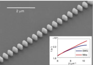
Here, we demonstrate using subwavelength grating (SWG) structures for refractive index engineering in mi-crophotonic silicon waveguides. A basic structure that exemplifies the use of refractive index engineering in a waveguide is shown in Fig. 1. This is a nonresonant photonic structure formed by etching a linear periodic array of rectangular segments into a 260-nm-thick single crystal silicon layer of a silicon-on-insulator wafer. A 2-μm-thick bottom oxide (SiO2) layer separates the
waveguide from the underlying silicon substrate. The waveguide core is a composite medium formed by inter-lacing the high-refractive-index segments with a material of a lower refractive index, which at the same time is used as the cladding material. The refractive index of the core is controlled lithographically by changing the volume fractions of the two materials. By intermixing Si and SU-8 materials at the subwavelength scale, the re-fractive index range of ∼1:6–3:5 can be obtained.
In order to avoid the formation of standing waves due to Bragg scattering and the opening of a band gap near 1550nm wavelength, we chose the nominal structural period d ¼ 300 nm, which is less than a half of the effec-tive wavelength of the waveguide mode λeff. Indeed,
per-iodic photonic lattices have been investigated to a great extent, but the efforts have almost exclusively focused
on photonic crystals with d ∼ λeff=2 that have a band
gap at the operational frequency range [5]. In such struc-tures, a waveguide is created by introducing a line-defect in a periodic lattice. In contrast to photonic crystal waveguides, the light is confined in our SWG waveguide by total internal reflection, as in conventional index-guided structures.
Figure 1(inset) shows the dispersion diagram of our periodic SWG waveguide calculated using the MIT photo-nic bands software. We have determined that the disper-sion away from the bandgap resonance matches that of an equivalent strip waveguide with a core index of 2.65. Electron beam lithography was used to define waveguide patterns in hydrogen silsesquioxane resist. The patterns were then transferred into the silicon layer by inductively coupled plasma reactive ion etching. The samples were coated with a 2-μm-thick SU-8 polymer layer (upper clad-ding) with a refractive index of 1.58. We estimated the
Fig. 1. (Color online) SWG waveguide (SEM image). Inset, dispersion diagrams for SWG and an equivalent strip waveguide with an engineered core refractive index of 2.65 (TE polarization).
2526 OPTICS LETTERS / Vol. 35, No. 15 / August 1, 2010
SWG waveguide loss by coupling the light to a set of test waveguides of different lengths varying from 5 to 30 mm, located on the same chip, yielding the propagation loss of −2:1 dB=cm near the 1:55 μm wavelength. Counterintui-tive as it may seem that such low loss is achieved for light propagating over a 1 cm distance through more than 33,000 boundaries between high- and low-refractive-index segments, our finding is consistent with the Bloch theory for periodic structures. The group index was measured using Mach–Zehnder interferometer test struc-tures. We have determined a low, polarization indepen-dent and almost constant group index of ng∼ 1:5 over the measured wavelength range of λ ¼ 1480 nm− 1580nm, in agreement with simulation results. A major problem with both conventional and bandgap micropho-tonic waveguides is their large polarization dependent loss (PDL), and those waveguides are typically used for TE polarization only [5,6]. In our SWG waveguides, the PDL is below 0:5 dB.
We demonstrate the potential of SWG refractive index engineering through the realization of practical func-tional components. Our SWG coupler, shown in Fig. 2, is designed to reduce the effective index mismatch and the associated loss at the fiber–chip coupling inter-face. The coupler principle is based on a gradual modi-fication of the waveguide core refractive index and the corresponding mode size transformation by changing the volume fractions of the Si and SU-8 materials that form the composite waveguide core. The microscopic
geometry of the taper was designed such that at one end of the coupler, the effective mode index is matched to a 450-nm-wide silicon strip waveguide for both TE- and TM-like polarizations (nTE ¼ 2:51 and nTM¼ 2:11), while at the end near the chip facet, it is close to that of an op-tical fiber (n ∼ 1:5). We used a lensed single-mode opop-tical fiber with a Gaussian beam waist of 2 μm. Our previous theoretical study allowed us to identify the range of cou-pler parameters (grating period, chirp, duty ratio, taper length, and tip width) for adiabatic mode transformation with low loss and negligible higher order mode excitation [3]. The fabricated coupler structure is shown in Fig. 2. The grating period is linearly chirped from 400 nm at the chip edge to 200 nm at the junction with the strip wave-guide. At the same time, the waveguide width is tapered from 350 nm to 450 nm. Two taper stages with distinct geometries of silicon segments are used to account for different mode confinement in two regions of the cou-pler. In the first stage [Fig. 2(b)], near the chip edge where the mode is weakly confined, the gaps are fully opened and their lengths linearly decrease from 200nm to 170 nm. In the second stage [Fig.2(c)], near the strip waveguide where the mode is highly confined, we used silicon bridging segments to partially fill the gaps, thereby mitigating the loss by making the transition more adiabatic. In this region, the gaps have a constant length (100 nm), and the width of the Si bridging seg-ments linearly increases from 100 nm to 450 nm where the coupler joins the strip waveguide. The two taper stages can also be clearly seen in the intermediate region of the coupler shown in Fig.2(d).
Transmission spectra of the coupler structure mea-sured using a tunable semiconductor laser are shown in Fig. 2(e), for the wavelength range (1430–1630nm), which exceeds the full S, C, and L telecom bands. The curves represent the measurements of a 5-mm-long sili-con strip waveguide terminated with the SWG couplers at their inputs and outputs, for TE (blue) and TM (red) po-larizations. For this structure, a coupling enhancement of ∼16 dB is measured, compared to the reference wave-guide without the SWG tapers (near λ ¼ 1550 nm, TE po-larization). The insertion loss in Fig. 2(e) includes the coupling loss and the propagation loss in the strip wave-guide. The intrinsic coupler loss was determined in an independent measurement using a broadband Er-fiber source on a series of couplers (up to 62) connected back to back as −0:23 dB for TE and −0:47 dB for TM polar-izations [see inset of Fig.2(e)]. The low intrinsic coupler loss is important, as it allows a seamless integration of the silicon strip and SWG waveguides in a photonic cir-cuit. From the measured insertion loss, the waveguide propagation loss, and the coupler intrinsic loss, the total fiber-to-waveguide coupling efficiency was determined as −0:9 dB for TE and −1:2 dB for TM polarizations. To our knowledge, this is the highest efficiency with minimal wavelength and polarization dependence yet re-ported for a microphotonic coupler [7]. Furthermore, the SWG coupler exhibits a high tolerance to the feature size variations that may arise from limited accuracy of litho-graphy and etching. We found that the coupler loss is neg-ligibly affected by changing the taper tip width from the nominal 350 nm to 300 nm, with loss penalty of less than 0:1 dB for both polarizations. This is a remarkably
Fig. 2. (Color online) SWG input coupler. (a) SEM image of the coupler. (b) Low-confinement section near the chip edge. (c) High-confinement section near the 450-nm-wide strip wave-guide. (d) Intermediate section positioned at ∼15 μm from the chip edge. (e) Transmission spectra of the insertion loss of a strip waveguide terminated at both ends with a SWG coupler, for TE (blue) and TM (red) polarizations. The inset shows the intrinsic coupler loss measured on a series of couplers con-nected back to back.
improved fabrication robustness compared to other cou-pler designs.
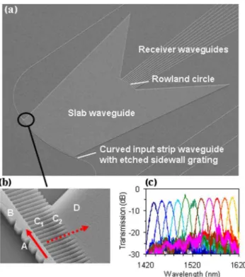
As we showed above, in silicon-based waveguides, media with a wide range of intermediate effective indices can be engineered by modifying the volume fractions of the silicon and cladding material. This control of the re-fractive index in a specific location of a chip is highly de-sirable for building sophisticated microphotonic circuits, as in the example of the optical multiplexer circuit shown in Fig.3(a). This new device is only possible using a SWG-engineered nanostructure that provides sufficient optical confinement to make a waveguide, yet have a waveguide boundary that is transparent to light propagating normal to the boundary. In this multiplexer, the light propagating in the curved strip waveguide is diffracted by the grating etched in one of the waveguide sidewalls [Fig.3(b)]. Cur-ving the waveguide serves the focusing function, so that diffracted light propagates with a convergent wave-front toward the focal region. Different wavelengths are focused at different positions along the focal curve
(Rowland circle of radius 80 μm) where they are inter-cepted by the receiver waveguides. Our previous theore-tical study allowed us to calculate design parameters to minimize cross talk and diffraction loss [8]. The sub-wavelength nanostructure (similar to that reported in [9]) formed in the trench between the strip waveguide and the slab waveguide combiner is shown in Fig.3(b). The purpose of using the subwavelength trench is two-fold: near the strip waveguide an effective material index of n ∼ 2:03 is created (300 nm SWG pitch, 50% duty ratio, TE polarization). Here, the trench acts as a waveguide for light diffracted by the grating toward the combiner re-gion, while acting as a lateral cladding for the strip wa-veguide. On the other side of the trench, near the slab waveguide combiner, a triangular SWG structure is used as a graded-index medium to suppress Fresnel reflection for the light propagating from the trench to the slab wa-veguide. Transmission spectra for 11 channels of the spectrometer are presented in Fig. 3(c). The achieved maximum-to-minimum transmission ratio is as large as ∼20 dB, while the loss is approximately −4 dB, allowing for wavelength filtering with a bandwidth of 170 nm. This is the largest wavelength range yet reported for a minia-ture spectrometer chip. Remarkably, this performance is achieved for a device size of only ∼160 μm × 100 μm.
We demonstrated refractive index engineering in a microphotonic waveguide using SWGs, including im-plementations in practical components at telecom wavelengths. Our technique circumvents an important limitation in integrated optics, that is, the fixed value of the refractive indices of the constituent materials. These results suggest that SWG waveguides could be-come important elements for future integrated photonic circuits.
References
1. I. E. Tamm and V. L. Ginzburg, Izv. Akad. Nauk SSSR Ser. Fiz. 7, 30 (1943).
2. J. N. Mait and W. W. Prather, eds., Selected Papers on Sub-wavelength Diffractive Optics, SPIE Milestone Series, V. Ms 166 (SPIE Press, 2001).
3. P. Cheben, D.-X. Xu, S. Janz, and A. Densmore, Opt. Ex-press 14, 4695 (2006).
4. J. H. Schmid, P. Cheben, S. Janz, J. Lapointe, E. Post, A. Delâge, A. Densmore, B. Lamontagne, P. Waldron, and D.-X. Xu, Adv. Opt. Technol. 2008, 685489 (2008). 5. T. J. Krauss, R. M. DeLaRue, and S. Brand, Nature 383,
699 (1996).
6. F. Xia, L. Sekaric, and Y. Vlasov, Nat. Photon. 1, 63 (2006). 7. V. R. Almeida, R. R. Panepucci, and M. Lipson, Opt. Lett. 28,
1302 (2003).
8. P. J. Bock, P. Cheben, A. Delâge, J. H. Schmid, D.-X. Xu, S. Janz, and T. J. Hall, Opt. Express 16, 17616 (2008). 9. R. Halir, P. Cheben, S. Janz, D.-X. Xu, Í. Molina-Fernández,
and J. G. Wangüemert-Pérez, Opt. Lett. 34, 1408 (2009). Fig. 3. (Color online) Waveguide grating multiplexer with
re-fractive index engineered SWG interface. (a) Fabricated multi-plexer chip. (b) Detailed view showing several grating teeth (A) etched in a sidewall of strip waveguide (B) along with SWG na-nostructure (C1) joining the slab waveguide (D) via a
graded-index antireflective SWG interface (C2). The arrows indicate
the light propagation direction in the strip waveguide (solid ar-row) and light diffracted (dashed arar-row) by the sidewall grating into the slab waveguide region via the SWG interface. (c) Mea-sured multiplexer spectra.