Design, implementation, and verification
of
a
multipurpose, flexible, three-phase back-to-back
voltage-source inverter
by
Elaina T. Chai
B.S., Massachusetts Institute of Technology (2012)
Submitted to the Department of Electrical Engineering and Computer
Science
in partial fulfillment of the requirements for the degree of
Master of Engineering in Electrical Engineering and Computer Science
at the
MASSACHUSETTS INSTITUTE OF TECHNOLOGY
February 2014
©
Elaina T. Chai, MMXIV. All rights reserved.
The author hereby grants to MIT permission to reproduce and to
distribute publicly paper and electronic copies of this thesis document
in whole or in part in any medium now known or hereafter created.
Signature redacted
A uthor ...
...
Department of Electri l Engineering and Computer Science
"/
yIl-1
Certified by...
Signature redacted
January
it, ZU14
Signature redacted
Ivan Celanovic
Principal Research Scientist
Thesis Supervisor
Accepted by.
...
Albert R. Meyer
Chairman, Masters of Engineering Thesis Committee
OF TECHNOLoGY
JUL 15 2014
Design, implementation, and verification of a multipurpose,
flexible, three-phase back-to-back voltage-source inverter
by
Elaina T. Chai
Submitted to the Department of Electrical Engineering and Computer Science on January 31, 2014, in partial fulfillment of the
requirements for the degree of
Master of Engineering in Electrical Engineering and Computer Science
Abstract
In this thesis, I designed, implemented, and verified a multi-purpose,three-phase back-to-back voltage source inverter for grid connected applications. This inverter features extensive hardware protection, opto-isolation between the power stage and the con-troller, and reconfigurable I/O routing. The converter is designed for both research and teaching to enable rapid prototyping and verification of advanced control algo-rithms for grid-connected converters, motor drives etc. I also demonstrate the utility of the power electronics converter as a vector controlled PMSM motor drive. Finally, I use the inverter to perform frequency domain validation of a hardware-in-the-loop simulator. I then design and implement a virtual spectrum analyzer, whose imple-mentation required the creation of a DFT algorithm in python based on the Goertzel algorithm.
Thesis Supervisor: Ivan Celanovic Title: Principal Research Scientist
Acknowledgments
I would like to first and foremost, express my sincere gratitude to my mentor and
thesis supervisor, Ivan Celanovic, for his knowledge, patience and guidance. He has been, and continues to be a pillar of support during my years spent working for him as an undergraduate researcher and as a Master's student, as was critical to the successful completion of my thesis.
I would also like to thank my lab mates, Jason Poon, Michel Kinsy and Walker Chan, for their advice, company, pranks and stories. They made every day working in the lab something fun to look forward to, and they were invaluable in their advice towards my work.
Last but not least, I would like to thank my family: my parents Ronald and Suzanne, for their support and their patience, especially during the times I was too grumpy and tired to talk to; my older sister, Sarah and her awesome baked goods always waiting for me when I go home for the holidays, and my twin Lauren, for putting up with moods in proxy of my parents, and reminding me to have fun once in a while.
Contents
1 Introduction 1.1 Thesis Contributions . . . . 2 Inverter Design 2.1 Power Stage . . . . 2.1.1 IGBT Module . . . . 2.1.2 Voltage and Current Measurements2.1.3 DC Measurements
2.1.4 Isolated Power Mod
. . . .
uiles . . . .. . . .
. . . .
. . . .
. . . .
2.2 Flexible I/O 2.3 Protection Scheme . . . 2.3.1 CPLD protection 2.3.2 DSP Protection 2.4 Layout Considerations 2.5 Digital Stage . . . . 2.6 Finished Packaging . . . 2.7 Experiments . . . . 2.8 Conclusion . . . . 2.8.1 Issues . . . . 2.8.2 Final Remarks .3 Virtual Spectrum Anayzer
3.0.3 Previous Works .
in Real-Time HIL Simulator
15 16 19 . . . . 2 0 . . . . 2 1 . . . . 2 2 . . . . 2 3 . . . . 2 4 . . . . 2 5 . . . . 2 6 . . . . 2 9 . . . . 2 9 . . . . 3 0 . . . . 3 2 . . . . 3 3 . . . . 3 4 . . . . 3 6 . . . . 3 6 . . . . 3 6 39 . . . . . 40
.
. . . .
.
3.0.4 Introduction . . . .4
3.1 Frequency Domain Analysis of HIL Simulator . . . . 41
3.1.1 Test Setup . . . . 42
3.1.2 Input Impedance Experiment . . . . 43
3.1.3 Output Impedance Experiment . . . . 44
3.1.4 Line-to-Output Experiment . . . . 45
3.1.5 Control-to-Output Experiment . . . . 46
3.1.6 Loop-Gain Measurement . . . . 48
3.2 Reference Hardware Design . . . . 50
3.3 Fidelity Comparison: HIL vs Reference Hardware Design . . . . 52
3.3.1 Time Domain Comparison . . . . 52
3.3.2 Frequency Domain Comparison . . . . 54
3.4 Conclusion . . . ... . . . . 55
4 Conclusion 57
A Inverter PCB Layout 59
B Mechanical Design Drawings 67
C Back-to-Back Inverter Pin 10 71
D Inverter Circuit Schematic 75
E CPLD Pin 10 85
List of Figures
2-1 Top Level Schematic of Inverter . . . . 21
2-2 Platform Cable USB II for programming the CPLD . . . . 26
2-3 Programming the CPLD . . . . 26
2-4 Comparator circuit for fault detection . . . . 28
2-5 Layer 2 of PCB showing separation of ground planes . . . . 32
2-6 Image of Inverter Front Panel interfacing with microcontroller board . 33 2-7 Image of Inverter Back Panel . . . . 34
2-8 Image of PMSM Test Setup . . . . 35
2-9 Transient Line Current comparisons of inverter hardware ( i"(t) in blue) and the real-time emulation (i, in cyan) Error shown in red. . 35 2-10 Steady-state Line-to-Line Voltage comparisons of inverter hardware ( Vab(t) in blue) and the real-time emulation (i'ab in cyan). . . . . 35
3-1 Schematic of Input Impedance Measurement (controller is external) . 43 3-2 Bode Plot of Buck Converter Input Impedance . . . . 44
3-3 Schematic of Output Impedance Measurement (controller is external) 44 3-4 Bode Plot of Buck Converter Output Impedance . . . . 45
3-5 Schematic of Line-to-Output Measurement (controller is external) . . 46
3-6 Bode Plot of Buck Converter Line-to-Output transfer function . . . . 46
3-7 Model of Buck Converter simulated in real-time, as shown interfac-ing with an open-loop embedded controller to measure the control-to-output transfer function . . . . 47
3-9 Schematic of Loop Gain Measurement . . . . 49
3-10 Bode Plot of Closed Loop Buck Converter Loop Gain transfer function 50 3-11 Schematic of Buck Converter validation setup, as shown interfacing with an open-loop embedded controller to measure the control-to-output transfer function . . . . 51
3-12 Photograph of the experimental buck converter HIL emulation valida-tion setup . . . . 51
3-13 Comparison of steady state output voltage, V0t of the HIL emulator and the reference hardware design . . . . 53
3-14 Comparison of steady state inductor current of the HIL emulator and the reference hardware design . . . . 53
3-15 Comparison of control-to-output measurements between the HIL em-ulator and the reference hardware design . . . . 54
A-1 Layer 1: Signal . . . . 60
A-2 Layer 2: Ground Plane . . . . 61
A-3 Layer 3: Signal
/
Power . . . . 62A-4 Layer 4: Signal
/
Power . . . . 63A-5 Layer 5: Ground Plane . . . . 64
A-6 Layer 6: Signal . . . . 65
B-i Mechanical Drawing of Heat Sink for Grid-Connected IGBT, IGBT1 68 B-2 Mechanical Drawing of Heat Sink for Load-Connected IGBT, IGBT2 69 D-1 Schematic of CPLD Connections . . . . 76
D-2 Schematic of Analog and Digital Connectors . . . . 77
D-3 Schematic of Power Stage 1 . . . . 78
D-4 Schematic of Power Stage 2 . . . . 79
D-5 Schematic of Analog Signal Conditioning Circuits . . . . 80
D-6 Schematic of Power Supplies and Output Filters . . . . 81
List of Tables
2.1 PMSM Experimental Testbed Specifications and Ratings . . . . 34
3.1 Component values for buck converter simulation test setup . . . . 42
3.2 Real-time HIL computational platform features . . . . 43
3.3 Component values for buck converter test setup . . . . 51
C. 1 Table showing Pinout of 64-Pin Analog Connector . . . . 72
C.2 Table showing Pinout of 96-Pin Digital Connector . . . . 73
Chapter 1
Introduction
This thesis presents the development of hardware and software tools for the purpose of rapid controller development for controlling power electronics systems. This thesis will be presenting a flexible back-to-back 3-phase inverter for the purpose of reference hardware validation of controller design, and a virtual spectrum analyzer for imple-mentation inside a ultra-low-latency hardware in the loop (HIL) power electronics simulator.
Power electronics is a discipline that deals with efficient conversion and control of power flow by means of semiconductor switches; whether it is DC-DC conversion inside a computer, or DC to 3-Phase AC interface with the power grid. With over $400 billion spent on electrical energy in the US alone in the last year, more reliance on 'green' energy, and increasing costs associated with extracting energy from other sources such as fossil fuels, any increase in efficiency and reliability introduced into power electronics will result in massive energy savings. Some estimates predict up to
30% energy savings by power electronics if fully utilized.
power electronics research. However, power electronics systems are not very easy to model compared to other electronic systems. Most electronic systems can be very accurately modeled by assuming that the entire system is linear time invariant (LTI). By assuming an LTI system, analysis and predictions of the behavior of the system becomes much simpler, and one can take advantage of a large range of available mathematical and computational tools. Power electronics circuits heavily rely on the use of fast switches which are inherently non-linear. Every time a switch changes its state, the topology of the circuit changes. As a result, the entire power electronics system is a non-linear time-varying dynamic circuit.
To model power electronics systems, ideal switch models are often a good approx-imation. For a circuit with n switches, the set of possible states of the circuit can be as high as 2n (though the actual number of valid states is lower). Within each of these states (we call them modes in hybrid system terminology) however, the topology is approximated as an LTI system, easing the analysis. The only difficulty is that one has to keep track of these modes.
1.1
Thesis Contributions
Thesis contributions are two fold:
1. The design, construction and verification of the inverter
2. The design and implementation of the spectrum analyzer inside the real-time emulator.
For the inverter design and construction, I will describe the following contribu-tions:
* Top Level design of inverter
" 3 level Scheme to protect the user and hardware against a wide variety of fault conditions
" Line and DC Measurements to allow for closed loop control of the system " Flexible Digital I/O using a CPLD
" Mechanical Design of the system
" Layout considerations to improve noise effects
For the spectrum analyzer, I will describe the followign contributions:
" Implementation of the spectrum analyzer " Test Setup and verification
Chapter 2
Inverter Design
My project was to create a universal bi-directional back-to-back 3-phase 2-level
in-verter to serve as the flexible hardware prototyping for advance control development, to be used in conjunction with the TI DSP controller. The inverter is designed to be used in a research and academic settings.
The project is a new design inspired by an inverter built by Nathan Pallo for his 2011 Undergraduate Advanced Project, titled 'Hybrid Dynamical Modeling of Power Electronics Systems'[10]. He designed a single three phase 2-level inverter. The nominal output was a phase voltage of 120V, and phase current 12A. The switching for the 3-phase inverter was implemented using an IGBT module by International Rectifier rated for 600V 20A. The design featured full isolation between power and small signal circuitry for EMI and safety reasons. He used analog opto-isolators for output current and voltage measurements, and BNC connectors to connect these measurements to the external controller. Digital isolators were used for the gate drive signals. These digital signals were delivered to the board via a DB-37 connector. The final PCB was very compact. The PCB itself was 16 square inches, and supported only with standoffs. It was not designed to be encased in an enclosure. Additional
breakout boards were required to interface with the controller.
My revision features key improvements in the original design by Nathan, to be
discussed later in this report, such as:
1. 3-level Protection scheme for hardware and user
2. Integrated Power supply for control and signal conditioning circuitry
3. Improved DSP controller interface
4. Increased EMI suppression
5. Increased current and voltage filtering 6. Flexible digital 10
7. Mechanical Packaging
The inverter is designed to be used in as the final verification step of a rapid prototyping design process and as a teaching tool. The control design process is described as follows:
1. Initial control design and testing using an offline simulator (e.g. PSIM or PLECS)
2. Rapid protyping using ultra-high fidelity HIL system
3. Final control system verification using flexible three-phase two-level
back-to-back IGBT inverter.
2.1
Power Stage
In this section I will describe the power stage of the inverter. I will elaborate on the features, choice of key power components, as well as PCB layout. A top level schematic of the inverter is shown in Figure 2-1.
13-Phase Power
i/O
Grid Connected Side
... ... ...
....
....
...
---
49
... ...
... ....
... ...
...
--
----F, -n-aiog isol
I
DC Power 1/0
6f-k3-Phase Power 1/01
Load Connected Side
--
--
-
----
----
--- [-
--...---- - O o
jagx:1
Gate Drivers/Isolation
Signal
Coditio
g
Fault Protection
CPLD
Analog
1/O
Digital I/O
Figure 2-1: Top Level Schematic of Inverter
2.1.1
IGBT Module
The power module used is the an intergrated 3-phase IGBT module by International rectifier, IRAMY20UP60B, rated for 600V 20A[4]. To create the 2-level inverter, two of these modules were connected via the DC bus, as shown in Figure 2-1.
An integrated power module was chosen because of the additional functionality and convenience that accompanies a complete module package. The inverter itself could have been constructed using 12 switches (6 per inverter) at a potentially lower total cost than the integrated module. However, having the switches in a single module, the overall layout of the switches is much tighter than what could easily be achieved by 6 individual switches. In addition, this power module has highly
I
desirable functionality and built-in protection that would have been otherwise difficult to implement otherwise. This protection includes:
1. Shoot-through protection.
2. Over-current and over-temperature protection.
Additionally the module provides temperature measurement as well as a DC-link current measurement.
2.1.2
Voltage and Current Measurements
This section describes the measurement circuits on the 3-phase line sides of the in-verter. Both sides feature current measurement circuits on two of the three lines. The current measurement of the third line can be calculated from the other two. The grid-tied side of the circuit also has circuits to measure the line-to-line voltages. This side is the side intended to be connected to the grid if the application calls for it (see left side of figure 2-1).
Having these measurements is crucial in many standard applications of 3-phase inverters. For example, in the application of pernament magnet synchronous motor (PMSM) drive, proper control can be achieved using closed loop control where the feedback signals are the phase current measurements. In grid-connected applications, such as a photo-voltaic circuit injecting power into the grid, in order to efficiently inject power into the grid, the phase and amplitude of the line-to-line grid voltage must be known by the controller.
The key modules used to make the current and voltage measurements are a series of current and voltage Hall Effect transducers, listed below:
1. Current Transducer - CAS 15-NP [6].
2. Voltage Transducer - Mfg. No. LV 20-P [5].
These modules were chosen for a number of reasons. They were very simple to integrate and their nominal measurement ranges easily captured to expected current and voltage ranges of the power stage. Additionally, they could provide measurements that were both bi-directional, as well as isolated, elimnating the need for special analog opto-isolation circuits to deliver the measurements to the small-signal analog stage.
2.1.3
DC Measurements
This subsection describes the DC bus measurements. The measurements are as
fol-lows:
1. DC-Link Current through IGBT Module 1 (using integrated shunt resistor)[4].
2. DC-Link Current through IGBT Module 2.
3. DC Bus Voltage.
These measurements are important for two reasons: closed loop control and circuit protection. In certain applications, such as a boost rectifier, where the output voltage is the DC Bus voltage, the goal is to maintain a certain output voltage via feedback measurements to the micro-controller.
Additionally, in case of fault, it is essential to monitor the the DC bus and DC-Link current being carried by the components. The 3-stage protection scheme implemented in this design, requires that both CPLD and and the micro-controller have ready access to these values in order to initiate a safe shutdown of the circuit if need be. This is described further in section (ref).
2.1.4
Isolated Power Modules
The control the internal
and measurement circuitry in the power stage is supplied separately by isolated power supply. The voltages required are as follows:
* +5V
* -5V * +12V * +15V
Being connected to the power stage comes with two main disadvantages. The first is that power electronics circuits are very noisy, especially compared to relatively small signal analog circuits. The second, is the high power nature of power electronics presents a hazard to any electronics directly connected to it. Without proper isola-tion, even through the power supply of the board, any faults in the power stage can potentially destroy not only the power supply, but any delicate circuitry such as the control boards, as well as present a hazard to the connected computer as well user, who will be directly interacting with the control board more than any other system connected to the inverter. It is for this reason that special isolated power modules
are required to power the circuitry in power stage.
To further reduce the problem of noise, the measurement circuitry is given its own analog ground inside the power stage, and a +5V and -5V power module separate from the rest of the circuitry inside the power stage. The grounds are separated by a ferrite bead[12]. The final list of components are as follows:
Part Description
+5/+15V Isolated Power Module
+12V Isolated Power Module
+5/-5V
Isolated Power ModuleManu. Murata Murata CUI Inc Manu. Number NMD050515SC MEV3SO512SC VASD1-S12-D5-SIP Ratings 1OOmA,34mA 250mA 100mAlOOmA
2.2
Flexible
I/O
To maintain compatability with as many controllers as possible, without the use of any additional breakout boards, it was necessary to insert a programmable device that could do the rerouting of these digital signals. The device chosen was the CPLD, and with it, the inverter system can be rapidly programmed to accept either controller, or any other that uses the same DIN connector.
The part chosen was the XCR3128XL-10VQ100C by Xilinx, a 100-pin CPLD with
a max delay of 9.1ns and 84 general purpose I/O[16]. The pin connections of this part can be found in table E.1.
As long as the controller uses the 96-pin DIN 41612 connector, and has its I/O along the 43 pins connected to the CPLD, the CPLD can be programmed to route the appropriate signals.
There are two minimum requirements for programming the CPLD:
9 ISE WebPack, a Xilinx programming environment free for use for programming
CPLD's.
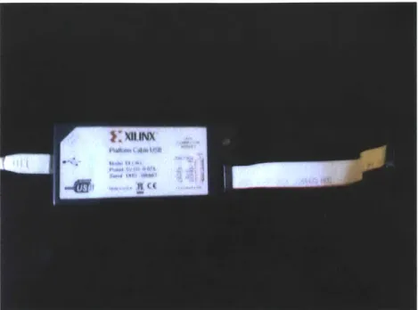
9 JTAG programmer. The recommended model is the Xilinx Platform Cable USB II, shown in figure 2-2, and uses a 14-pin 2mm female connector.
Figure 2-2: Platform Cable USB II for programming the CPLD
Figure 2-3: Programming the CPLD
2.3
Protection Scheme
Protection schemes are essential to power electronics design. The large currents and
voltages regularly handled by power electronics systems not only present a danger
to any connected circuitry, but also pose serious health hazards to the user and any other by-standers. In this design, we handle this by using relays, fuses and other components to implement a 3-level protection scheme:
" Fast: Within ps, the IGBT module internal protection starts shutting down the IGBT and the CPLD throw open all relays.
" Average: Fast-acting fuses ( as quickly as 10ms) disconnect the power stage[7].
" Slow: External controller shuts down PWM and signals that contactors should open.
The scenarious we are interested in protecting against are:
1. DC-Bus Overvoltage 2. DC-Bus Undervoltage
3. Over-current in each IGBT module 4. Over-temperature in each IGBT module 5. Shoot-through
They first four scenarios produce 6 signals (2 each for current and over-temperature) that are measured via a series of comparators, whose reference values can be set by potentiometers. In the event that we encounter one of the above scenarios, the comparator would transition to a high state, and initiate a shutdown sequence (See Appendix D pg. 83). Figure 2-4 shows the comparators on the board with their associated potentiometers for setting the reference values.
Figure 2-4: Comparator circuit for fault detection
In the case of over-voltage, the CPLD immediately turns on a chopper circuit(See Appendix D pg. 79). This consists of a power resistor and switch (at the same rating as the IGBT modules) across the DC bus. It will immediately start drawing power from the DC bus when DC Link Overvoltage is detected, and will shutoff when the
DC Link has recovered from over-voltage.
The IGBT module currently used (iramy20up6Ob) does not contain an input for a shutdown signal. Instead it already comes with the following protection schemes built in:
" Over current protection " Over temperature protection
2.3.1
CPLD protection
The output of the comparators for the above signals are tied directly to CPLD I/O pins. Within the CPLD, this signals would be a connected to a single OR gate. When we encounter any of the above fault scenarios, the CPLD will initiate the following shutdown sequence:
1. Turn off all PWM signals.
2. Throw open all contactors.
3. Send a fault signal to the DSP.
4. Turn on an LED to indicate to the user that a fault was detected.
2.3.2
DSP Protection
While the DSP controller will receive the analog outputs of the the Inverter, and so can actually measure when the module has encountered one of the above fault scenarios, this detection is slower, compared to the built-in module protection. Instead the module will rely on the fault signals from the CPLD to initiate a shutdown. Upon receiving the fault signal it will shutdown the PWM signals.
Due to the large capacitance across the DC bus, it is a good practice to place a discharge resistor across the DC bus capacitor. This will ensure a speedy discharge of the large bus capacitor ~10s when the converter is off. However, since we do not want this resistor to draw too much current during normal operation, the resistor chosen will have the following parameters:
* 20 K Ohms * loW
Fuses are mounted into the back panel of the case. They are added to the external connectors that serve as power I/O's, totalling 4 panel mount fuses.
2.4
Layout Considerations
One of the greatest challenges of the inverter design was the board layout. While certain factors such as proximity to external connectors, or the physical limitations imposed by the component sizes and the case dimensions played a role, by far, the factor that had the greatest effect on the board layout was noise considerations.
The problem was that the circuit board was a combination of three types of circuits:
" Analog " Digital
" Power switching (high-power)
The small signal analog stage circuits were all the circuitry whose job was signal measurement and conditioning. The digital stage was all circuitry expected to handle digital signals, and the power stage contained all circuitry connected to the high power electronics. While the rapid switching of digital circuits can produce some noise in the ground, the main source of noise is from the power stage, where the high currents flowing through the power electronics can induce noise in the nearby copper.
To minimize the effects of this noise, the ground was separated into 4 parts:
* Small signal analog: All analog circuitry used for conditioning of signals going out of the Analog I/O connector.
" Digital Stage: All circuitry used for routing of digital signals.
" Power electronics: All circuitry connected to the power electronics that either handles high power or digital signals.
" Small signal analog in power stage: All of the circuitry in the power stage used to capture measurements.
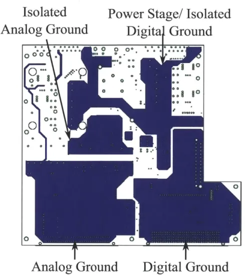
The amount of noise generated by the power stage was creating too much interfer-ence with the measurement circuitry to produce clean useful signals. To mitigate this as much as possible, the board had to be laid out in such a way that even the mea-surement circuitry and the rest of the power stage were given separate grounds and power supplies, connected only by a ferrite bead. Figure 2-5 shows ground separation in one of the inner layers.
The result of this layout is a 6-layer board, with most of the internal layers used for power routing, leaving the outer layers for signal routing. While it usually good practice to keep as many components as possible on one side of the board to reduce board manufacturing costs, this rule of thumb had to be broken to keep the power electronics compact, and the filter capacitors as close as possible to their respective power modules.
There is still some noise in the lOOmV range of the measured signals due to the power electronics, and this will simply have to be accounted for in system controller.
Isolated
Power Stage/ Isolated
Analog Ground
Digita Ground
I
0 00
Analog Ground
Digital Ground
Figure 2-5: Layer 2 of PCB showing separation of ground planes
2.5
Digital Stage
The addition of the digital stage is a major improvement over previous 2011 design.
The key component of the digital stage is the Complex Programming Logic Device
(CPLD), through which all digital I/O from the external connector is routed. This
component enables both the 3-level protection scheme, as well as the greatly increases
the overall flexibility of the unit.
* 1MHz clock
* 6 general purpose LED's drive by the CPLD
* Digital optoisolation circuits for all signals routed to the power stage * 6 Digitized signals from the analog stage for fault detection
2.6
Finished Packaging
The inverter was mounted in a plastic case by Bopla. The front and back panels are 2mm aluminum plates cut to provide openings for the external connectors, to provide mechanical support for the IGBT heat sinks, and a mounting platform for the fuses and the power supply.
Power Fuses for grid-connected side
3-Phase Connecto for Loads
irid Connected i-Phase Connector
Figure 2-7: Image of Inverter Back Panel
2.7
Experiments
After the completion of the inverter, it was used in test and verification experiments [2]. One such experiment was to control a permanent magnet synchronous machine (PMSM), and the results were compared with the real time emulator. The ratings for the PMSM are as follows:
Model identifier Anaheim EMJ-04APB
Stator Resistance 2.174 Q
Magnet flux linkage 0.3859 Wb
d-axis inductance 2.5 mH
q-axis inductance 2.5 mH
Number of Pole Pairs 2
Base speed 5000 r/min
Phase Current 2.7 A
Phase voltage 200 V
PWM Switching Frequency 4 kHz
Dead time 1 ps
Table 2.1: PMSM Experimental Testbed Specifications and Ratings
DC Bus Power Fuse
Figure 2-8: Image of PMSM Test Setup 0 4 3 2 1 0 -1 -2 -3 -4 -40 -20 0 20 40 Time (ms)
Figure 2-9: Transient Line Current comparisons of inverter hardware ( ia(t) in blue)
and the real-time emulation (Za in cyan) Error shown in red.
bi~ 0 0 V 200 100" 0 -100 -200 0 100 200 300 400 500 600 700 Time (us)
Figure 2-10: Steady-state Line-to-Line Voltage comparisons of inverter hardware
( Vab(t) in blue) and the real-time emulation (ibab in cyan).
S- -... ... . ... .. .. a ... ... ...1 ,... , - - -Vab(t)
...-.
I I. . . . .
2.8
Conclusion
2.8.1
Issues
There are still issues facing the current iteration of the design:
* Noise is still a big issue in the DC current measurement circuitry, and the switching action of the IGBT's can be easily seen in the background of the measured signals.
" The inverter cannot be directly connected to the grid, and still has to be powered by either a variable DC or AC supply. The concern is inrush through the AC
connectors.
Therefore my recommendations for any future revisions are the following.
For noise, consider having improved PCB layout and more finely tuned filtering.
To mitigate inrush on the 3-phase connectors, consider having another set of relays on the 3-phase legs, in series with resistors to pre-charge the DC-Bus cap to prevent inrush when connecting to the grid or a DC Bus pre-charging resistor.
From this project, I learned a great deal about the following:
2.8.2
Final Remarks
* Power electronics systems design
" Circuit schematic design " PCB Layout and Ordering
" Factors influencing component selection and availability " Power electronics safety
* Practical circuit construction and debugging techniques
I also became very adept at circuit CAD software, in this case, Eagle CAD, as well as the mechanical CAD software, Solidworks.
Chapter 3
Virtual Spectrum Anayzer in
Real-Time HIL Simulator
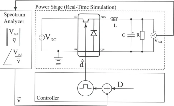
One of the key functions of the back-to-back inverter was to provide the final hardware validation of the experiments run using an Ultra-Low-Latency Hardware-in-the-Loop (HIL) simulator.
HIL has been receiving increasing attention as an indispensable tool for deisgn-ing and validatdeisgn-ing complex control systems. Hardware-in-the-loop enables control engineers to test real controller systems by directly interfacing them with a real-time emulation of a converter power stage. Because engineers are able to quickly test controllers under a wide range of operating and fault conditions without the need for a high-power lab, the amount of time and resources required for design, testing, and validation of these systems can be drastically reduced. In addition, the HIL configuration enables repeatable and formalized testing over a spectrum of operating conditions (including faults) that are often impossible or too expensive to test with real hardware.
3.0.3
Previous Works
Until recently however, the computational and latency requirements for real-time simulation of fast, non-linear switching power electronics have limited the speed, fidelity, and applicability of HIL emulators in power electronics. For instance, in [15], the authors have designed and tested a realtime HIL simulator of an H-bridge inverter. However, because the HIL simulation relied on a time averaged model with a minimum time step of 250[t s, the authors were unable to characterize the model beyond 100 Hz, which limits the fidelity of the model. In another study, authors have presented fast real-time HIL simulators with a minimum time step of 10s [3]. While they have validated the results of the system under steady state conditions, the
fidelity of the system for fast transient conditions and in the frequency domain have not been presented. Lastly, in [11], the authors have presented results under steady state and transient conditions for a real-time HIL simulator with a PWM sampling resolution of 12.5 ns and 10s simulation time step. However, the fidelity of this system in the frequency domain has not been validated, and it appears that the flexibility of the proposed modeling approach is limited.
The HIL emulator platform analyzed in this chapter is based on a novel application specific processor in FPGA that computes piecewise linear state space models in hard real-time with a 1its time step [8].
3.0.4
Introduction
In this chapter, I will:
9 demonstrate the concept and describe my implementation of a network analyzer in a high-fidelity HIL design environment.
" present a frequency domain analysis of several representative converter models in the HIL system by means of comparisons with small-signal analytical models. " describe an experimental test setup using the inverter described in the previous
chapter, to verify my findings in the time and frequency domains.
I experimentally validate several frequency domain transfer functions for a buck converter, including input impedance, output impedance, line-to-output, and control-to-output transfer functions using an HIL-based spectrum analyzer. To the best of my knowledge, extensive frequency domain fidelity validation has not been reported for any ultra-low latency HIL emulators. In addition, I believe that the network analyzer utility in HIL can be an extremely useful tool for control engineers to quickly tune and optimize performance of a closed loop control system.
3.1
Frequency Domain Analysis of HIL Simulator
In order to validate the fidelity of the HIL emulator in the frequency domain, I have created a test setup where I measure the following frequency domain transfer func-tions: input impedance, output impedance, line-to-output, and control-to-output. I will briefly describe the test setup used to obtain the frequency domain measure-ments, the four experiments used to measure the transfer functions, and the analytical models used to compare the results.
I have chosen the converter under test to be the buck converter, due to its ana-lytical small-signal model being very well understood. However, the HIL system can be easily expanded to model more complex systems such as a two-level inverter.
3.1.1
Test Setup
The procedure for the tests was as follows: the buck converter was created inside the schematic editor of the HIL and assigned the values shown in Table 3.1. For each experiment, an external signal generator is used to inject a disturbance into the HIL emulator. The frequency of the disturbance is swept and the resulting analog waveforms from the emulator are captured on an oscilloscope for post processing. Post processing is initially carried out using Python. A script is used to extract the Discrete Fourier Transform (DFT) of the swept frequencies based on the Goertzel algorithm. The DFT of the output is compared to the input disturbance, and plotted against the analytical model in the frequency domain[2].
Output Resistance, R 5Q Output Inductance, L 1 mH Output Capcitance, C 100 tF Input Voltage, VDC 50 V PWM Switching Frequency 10 kHz Duty Cycle, D 50% Dead time 1 ps
Table 3.1: Component values for buck converter simulation test setup
The open loop control algorithm for the buck converter is implemented on a sep-arate DSP based Texas Instruments TMS320F2808 Control Card.
The signal generator used to generate the disturbance is an Agilent 33220A and is injected through an interface board between the TMS320F2808 Control Card and the HIL emulator. For the input impedance, output impedance, and line-to-output tests, the disturbance is routed directly to the HIL emulator and is used to drive the simulated disturbance source. For the control-to-output test, the disturbance is routed to the internal ADC module of the TMS320F2808, where it is used to perturb the control signal, as seen in Figure 3-7. The specifications for the HIL computational platform can be seen in Table 3.2.
FPGA Device Xilinx Virtex-5 ML506
Clock Speed 100 Mhz
ADC Sampling Rate 1 MSPS
DAC Sampling Rate 1 MSPS
Table 3.2: Real-time HIL computational platform features
3.1.2
Input Impedance Experiment
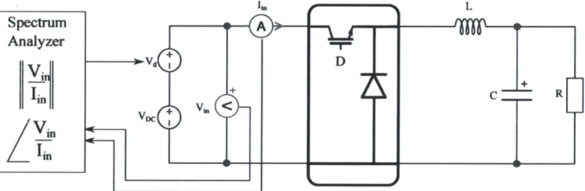
In the first experiment in which I measure the input impedance, I injected a distur-bance into the input voltage and measured the effect this disturdistur-bance had on the input current. A schematic of this is shown is Figure 3-1:
Ia
VDC+ V <
D
L
C R
Figure 3-1: Schematic of Input Impedance Measurement (controller is external)
The disturbance is modeled as a small sinusoidal voltage source in series with the
DC input voltage. The final voltage is shown in figure 3-1 as Vd. Indeed here I can see
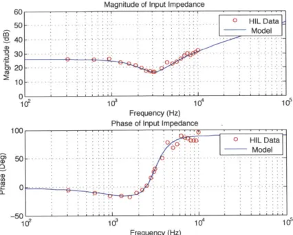
a benefit of using the HIL emulator system, in which there is no need for an isolation transformer or impedance matching in order to successfully inject our disturbance into the power electronics system. I compare this to the following analytical model shown in equation 3.1 [9] and plot the results in figure 3-2:
Vin 1 (s 2
RLC+sL+R
IinD2
(
sRC+ 1
Spectrum Analyzer V i (3.1)Magnitude of Input Impedance 50 40 30 20 10 0 1 100 0 -5' 02 1ic1 14 Frequency (Hz) Phase of Input Impedance
102 1le 10
Frequency (Hz)
Figure 3-2: Bode Plot of Buck Converter Input Impedance
3.1.3
Output Impedance Experiment
In this experiment, I injected a disturbance into the output current and measured the effect this disturbance had on the output voltage. The disturbance is modeled as circuit containing a small sinusoidal voltage source in series with a RC blocking circuit, in parallel with the output of the buck converter. A schematic of this is shown is Figure 3-3: I. A V1 L lout Cl RI AV C R < ou
T r
Vd Spectrum Analyzer Iout utLivowt
ZloutFigure 3-3: Schematic of Output Impedance Measurement (controller is external)
I compare this to the following analytical model shown in equation 3.2 [9] and
plot the results in figure 3-4:
V C) -o C U) 0 U) tl) 0 0) Co 0 0~ I -T-r-r%
'
L- - .0 a 0 HIL Data Model . . . . .. . . ....- -.. - -0 CP 0 HIL Data : Model ...-. . -...- :. 50| 1 9sLR s2RLC+sL+R 20 10 -W e 0
Magnitude of Output Impedance
0 HIL Data Model 103 4V2 12 o 0) 0 a,) 0 10 Frequency (Hz) Phase of Output Impedance
_50 1 An 102 103 Frequency (Hz) 10 (3.2)
Figure 3-4: Bode Plot of Buck Converter Output Impedance
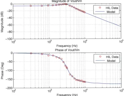
3.1.4
Line-to-Output Experiment
In the third experiment, in which I measure the line-to-output transfer function, I use the same setup as the input impedance experiment, but instead of measuring the input current, I measure the resulting output voltage to get the line-to-output transfer function. A schematic of this is shown is Figure 3-5:
This result is compared to the following analytical model shown in equation 3.3
[9] and plot the results in figure 3-6:
V tD 1 R (3.3) tin s2 LC + R +1 -10 r 1 1 0CP 0e - - -- - - - - -0 HIL Data .... Model 50
+ v Spectrum Analyzer
V
Vm I Ii C_ R Vu T<]Figure 3-5: Schematic of Line-to-Output Measurement (controller is external)
-o -o C (U 0) Q a, U, (U -c 0~ V -20 -40 -60 -80 -1 --1 Magnitude of VoutNin 00' 10 1 1 A 4 1 Frequency (Hz) Phase of VoutNin 0 0 HIL Data 50 - . . Model 00 -5 0 - .-no 10 le Frequency (Hz)
Figure 3-6: Bode Plot of Buck Converter Line-to-Output transfer function
3.1.5
Control-to-Output Experiment
For our fifth experiment, I inject our disturbance directly into the controller. The
ADC module inside the TMS320F2808 requires unipolar signals, so I inject this with
an offset. Inside the controller, I remove this offset and appropriately scale it before adding it to the value of the duty cycle inside the controller. An interrupt service routine runs at 8 kHz to read the ADC and update the PWM generator module inside the controller. The PWM module then uses this updated duty cycle value to determine the duty cycle of the PWM used to drive the converter.
0 I 0 HIL Data - Model -. . ...-. . . . .. . P id, 10 P
Spectrum
Analyzer
Vout
Z
ou
Figure 3-7: Model of Buck Converter simulated in real-time, as shown interfacing with
an open-loop embedded controller to measure the control-to-output transfer function
The corresponding analytical model in equation 3.4 [9]:
V
Vin
(dD s2LC+8L+ 1
(3.4)
However, the analytical model for the control-to-output transfer function has to be
modified to take into account the delay due to the PWM implementation of the
controller. This is unlike the previous frequency response measurements, in which
comparisons were made directly to the analytical models described in their respective
sections. Thus, the updated control-to-output transfer function is shown in equation
3.5, where T is the time step of the controller, and the real-time emulation is compared
to this model in figure 3-8:
(3.5)
e -r_ _
d
D
s2LC+8L+ 1Power Stage (Real-Time Simulation)
L
'DC
Vout
Magnitude of Vout/Control 50 E) 0 HIL Data Model -502 1010 104 105 Frequency (rad/s) Phase of Vout/Control 0 HIL Data -200 .. .. .. . ... . .. . ... . . M odel Q -400 -U -600 - --800 --1000 102 10 10 100 Frequency (rad/s)
Figure 3-8: Bode Plot of Buck Converter Control-to-Output transfer function
3.1.6
Loop-Gain Measurement
I tested the spectrum analyzer on a closed loop system to see if we could map out the loop gain transfer function. The system chosen was a TI online example closed loop buck controller code that used the output voltage as a feedback signal[13]. Instead of injecting the disturbance in the controller, within the emulator I injected the
dis-turbance Vd into the output voltage measurement V0st and used the sum of Vst + Vd
as the feedback signal to the external controller. The closed loop gain is measured as A schematic of this is shown in figure 3-9.
Vd
This approach is a marked improvement over the implementation in the previous section because this implementation of the spectrum analyzer is controller agnos-tic. The stock code from TI was run on the TMS320F2808 control card without
Real-Time Emulator I--- ---Vd Spectrum + Analyzer L V+ + VDC+ I out - -coupling TMS320F2808 Closed Loop Controller
Figure 3-9: Schematic of Loop Gain Measurement
any modifications. Instead the injection took place inside the emulator itself. The loop-gain transfer function can be mapped out independent of the controller hard-ware/software/firmware implementation, for rapid development of the closed loop parameters.
The prelimiary loop gain measurement result of this is shown in figure 3-10. We see a typical loop gain transfer function of the plant and the controller, with a slope at DC to mitigate steady state error, and a magnitude bump to improve bandwidth. Controller parameters are completely detuned and this measurement technique re-quires further test and verification, but overall results are promising.
E tM IA 4, Ma 9L 3U 25 20 15 10 5 0 -00 101 - -0 --- ...---. ...-. -. -. .... --- ... .. ... ---... ---- . --- - - -.. . . . ... ... ... ... ... . .... . .... .... .... .... .. .0. .. .... ...0 ...
0
2 101 Frequency (Hz) 101 00 0 ...-- -. ---- .... -- .... . .... 00 --- --- -- --0 --- -- -- - ---- ----.- -. .. 400 10 0 10 1 102 Frequency (Hz)Figure 3-10: Bode Plot of Closed Loop Buck Converter Loop Gain transfer function
3.2
Reference Hardware Design
To comprehensively validate the fidelity of the real time HIL emulation, I created a validation test setup that runs the real-time HIL emulation in parallel with an identical power stage implementation [2]. The schematic of this setup can be seen in Figure 3-11. The test setup can be seen in Figure 3-12 and the specifications of the test bed is given in Table 3.2 and Table 3.3.
101
Spectrum
Analyzer
V"
outV
t
Figure 3-11: Schematic of Buck Converter validation setup, as shown interfacing with
an open-loop embedded controller to measure the control-to-output transfer function
Figure 3-12: Photograph of the experimental buck converter
setup
HIL emulation validation
Output Resistance
10Q
Output Inductance
450 ptH
Output Capcitance
80 ptF
Input Voltage
50 V
PWM Switching Frequency
10 kHz
Inverter Module Ratings
20A, 600V
Dead time
1 pus
Table 3.3: Component values for buck converter test setup
Power Stage
________ IN*___ Cur+ LV
c -R
<
Cji
VoutController
The hardware reference design consists of the back-to-back two-level three-phase inverter drive described in the previous chapter.
3.3
Fidelity Comparison: HIL vs Reference
Hard-ware Design
In this section, I investigate the fidelity of the real-time HIL emulator by comparing the results of the large-signal time domain and the small signal frequency domain of the HIL emulator with the Buck Converter reference hardware design described in Section 3.2. The controller used is an open-loop Buck Converter control code run on the TMS320F2808 control card [14]. In each of the following experiments, I run both systems in parallel with the same PWM signals from the controller.
3.3.1
Time Domain Comparison
In the first experiment, I compare the steady state output voltage ripple of the HIL emulator with the real hardware reference. Figure 3-13 shows the comparison between the emulator and the real hardware reference on the time scale of the switching frequency.
In the second experiment, I compare the steady state current ripple through the inductor of the HIL emulator with that of the real hardware reference. Figure 3-14 shows the comparison between the two results. As the figures show, the emulation of the buck converter matches very closely with the real hardware reference on the time scale of the switching frequency.
30 25L . 0
0
..I ' -* HIL Emulator Real Hardware Error ... . . -. . . .. . . .. 20 . -15 -10 -.... 5 -. -. .. .. . .. . . . -0 -3.5 -3 -2.5 -2 -1.5 Tirre (s) -1 -0.5 0 x 10 Figure 3-13: Comparison of steady state output voltage,and the reference hardware design
:3 c U -3 5 4 3
Vst of the HIL emulator
HIL Errulator Real Hardware Error ..... .. . .. .. .. . . . .. .. .. . -. ....-. .-.-. ... -- .. .. . .... . . . .. . -2 1 0 -1 -3. 5 -3 -2.5 -2 -1.5 Time (s)
Figure 3-14: Comparison of steady state inductor current of the HIL emulator and the reference hardware design
-1 -0.5 0
x 10
3JI
..
-3.3.2
Frequency Domain Comparison
In the third experiment, I redo the small signal frequency domain experiment to measure the control-to-output transfer function, but this time I compare the results to the real hardware reference. Figure 3-15 shows the comparison in the frequency domain. As the figure shows, the emulation of the buck converter closely matches the frequency response of the real hardware converter.
60 2 40 > 20 0 1 0 (D 0 0)-200 a--400 1 Magnitude of Vout/Control 0 Hardware ---... ... - -0 .- - 06 " ' -- ..---. * HIL Data 234 0 10 10 10 Frequency (rad/s) Phase of Vout/Control S:0 Hardware * HIL Data - - -.. - .- .. . Y
0
10 10 10 Frequency (rad/s)Figure 3-15: Comparison of control-to-output measurements between the HIL emu-lator and the reference hardware design
3.4
Conclusion
For the initial frequency domain validation, post-processing was done using Mat-lab. With the concept of a network analyzer inside the real-time emulator validated against the back-to-back voltage-source inverter, the final spectrum analyzer inside the emulator was implemented using python and took advantage of the built-in cap-ture functions. The result is a seamless additional tool inside the emulator with which to carry out frequency analysis of the power electronics model in real time.
For this work I learned the following:
" Designing and implementing an experimental test bed. " Various techniques with which to carry out DFT analysis. " Automation script development for experimental purposes.
Another limitation is the variety of real-hardware frequency analysis comparisons we are able to implement. Many similar spectrum analysis of any power electronics systems usually requires injection using an isolation transformer. Our real-hardware comparison avoided this by injecting the distrubance signal into the controller itself, thereby avoiding physically tampering with the power electronics hardware. This limited the variety of real-hardware comparisons we could do, and a real-hardware comparison of the impedance measurements would require more powerful and spe-cialized hardware to inject the disturbance signal in a safe manner.
For future works, I recommend the following:
" Aquiring hardware to expand the range of hardware tests that can safely im-plemented.
control systems.
e A possible collaboration with RPI to use the virtual spectrum analyzer to carry out three-phase impedance measurements [1].
Chapter 4
Conclusion
In this thesis I have described a flexible multi-purpose back-to-back inverter with extensive built in software and hardware protection. I have demonstrated its utility in as both a power converter for a 3-phase PMSM, as well as a buck converter. I used the inverter as real hardware validation for my work validating the concept of a spectrum analyzer for a real-time simulator, which resulted in the complete python implementation of a spectrum analyzer tool for use inside the simulator software.
The specification for the back-to-back voltage source inverter with the following requirements:
" Flexible I/O for compatability with controllers used with the real-time simulator
* Extensive protection on a hardware and software level, due to its use in an experimental research setting
" Flexible power electronics stage to maximize the number of topologies it can
verify from the real-time emulator.
the implementation of spectrum analyzer inside the real-time emulator.
With the completion of both projects, the real-time emulator developers have a more flexible and safer hardware with which to verify their results from the emulator. Additionally, they now have a spectrum analyzer tool that can be implemented on their systems in real-time, further increasing the capability of their systems.
Such a tool can also be applied to future adaptive controller development projects, utilizing the results of the spectrum analysis to adjust parameters of the control code.
Suggestions for future work are:
* A next revision of the inverter PCB with improved PCB layout and more finely tuned filtering.
" consider having another set of relays on the 3-phase legs, in series with resistors to pre-charge the DC-Bus cap to prevent inrush when connecting to the grid, or a DC Bus pre-charging resistor.
" Aquiring hardware to expand the range of hardware tests that can safely im-plemented.
* Using the results of these tests in the development of adaptive closed loop control systems.
* A possible collaboration with RPI to use the virtual spectrum analyzer to carry out three-phase impedance measurements [1].
Appendix
Inverter PCB Layout
A
ado ma
amrw
-Figure A-1: Layer 1: Signal
13*
M.".C: I -JL. IV w w 04"-Cjm- -W G o0 0 a
0
T
17 7;
1
0000
0
0 .. 0. 0 000 o e 0 o 0 0000
0
o a i n0
S0
Nlo 0 A -0 * .. U a -00 .0 t7
3. *4 e . " n a 6 * a * U S 0 0*0 6*0 0*0 0*0 0 004 USOUS*UUOU 3.4 3541 . --. 4,' - ; 9 *** *"" " '...--...
0
EOGUSUCGUOUBO 0 0 0 0 no 0 0 a a 0a 0o n o 00 00o -, .. D wo 0 C. . 04: *.1...0. . Me ' " .. - - . S -wiern .aZaeU@ .-. U .Oh on moo @*"powwow Po.
Figure A-3: Layer 3: Signal / Power0
a.s
030 of I
o o o c
00 0 0 0 0 0 QOS * 5 0 0 .0
"m-
40
-0. S * -e-0
USD1
10
-
00 D Sgo 00 .S. 0
. 0 0 0 DO0 * so : a a hi US -, 00 .- - * - -**- U @ em istattineustUn.t.uttmotmu. o a!!!!ttitt!ttitRFigure A-4: Layer 4: Signal
/
Power a* ~0
S S S
Figure A-5: Layer 5: Ground Plane
. . e -.. U -_0 0