Chemical Nucleation of Diamond Films
Soumen Mandal,
*
,†Evan L. H. Thomas,
†Titus A. Jenny,
‡and Oliver A. Williams
*
,† †School of Physics and Astronomy, Cardiff University, Cardiff CF24 3AA, United Kingdom‡Department of Chemistry, University of Fribourg, Fribourg CH-1700, Switzerland
ABSTRACT: With the large differences in surface energy
between film and substrate in combination with the low sticking coefficient of hydrocarbon radicals, nanocrystalline diamond growth on foreign substrates typically results in poor nucleation densities. A seeding technique is therefore required to realize pinhole-free and thin coalescedfilms. In this work, a
chemical nucleation method for growth of diamond on nondiamond substrates based on 2,2-divinyladamantane is shown. After treating with the carbon-containing DVA, the chemically treated wafers were exposed to low-power-density plasma, known as the incubation phase, to facilitate the formation of diamond nucleation sites followed by a high-power-density growth regime to produce coalesced films. The resulting films demonstrate high crystallinity, whereas the Raman spectra suggest high-quality diamond with low sp2content.
KEYWORDS: diamond, chemical nucleation, chemical vapor deposition, diamond growth, adamantane
1. INTRODUCTION
For all but single-crystal iridium with its ability to dissolve and then expel carbon sufficiently fast for single-crystalline growth, diamond growth on foreign substrates typically results in polycrystalline diamond films.1,2 For example, the large differences in surface energy between diamond and silicon (6 vs 1.5 J cm−2) in combination with the low sticking coefficient of methyl precursors lead to the formation of three-dimensional clusters of density of 1× 10⁴to 1× 105cm−2upon growth on unseeded silicon.3,4To aid coalescence and produce thinfilms, a seeding step is therefore required to reach the nucleation densities required. In the literature a wide range of techniques can be found from mechanical abrasion of the substrate surface,5−7 ultrasonic particle treatment,8,9 bias enhanced nucleation10 and the attachment of nanodiamond particles onto the substrate surface11for subsequent growth. In addition, researchers have also tried nucleation of surfaces using chemical precursors like diamondoids.12−16 With the small size of diamondoid molecules (1 nm), successful use of such a seed would allow the growth of ultrathin layers of diamond on top of nondiamond substrates. However, although enhanced nuclea-tion was observed during these studies, the increase in density was not enough to produce thin coalescedfilms.17
With regards to the choice of chemical precursor, it was initially suggested by Olah18that organic molecules with cage structure can act as possible nucleation sites for diamond growth. The following years, Linford et al.19,20showed that it is possible to covalently attach organic molecules to the hydrogen-terminated silicon surface. This led Leroy et al.21to design adamantane based 2,2-divinyladamantane (DVA) for chemical nucleation of diamond consisting of the smallest diamondoid, adamantane (C10H16), with two vinyl groups to facilitate covalent attachment to the silicon surface. Giraud et al.22 were then able to demonstrate an increase in the
nucleation density above that of bare silicon upon using DVA, however coalescedfilms were not obtained.
It is to be noted that in many of the previous studies on the chemical nucleation of diamond growth the diamondoid molecules were spun-coated on substrates by dissolving in solvents like glycol15or toluene.16Therefore, it is important to investigate the effects these solvents have on the nucleation density on the substrates. For example, in the course of the present study, it was found that solvents like toluene or cyclohexane can also lead to enhanced nucleation on silicon substrates, in agreement with results reported within previous studies.23,24As a result, such solvent-mediated nucleation sites may interfere with diamondoid based chemical nucleation.
The main motivation for a chemical-based nucleation process is to develop a protocol that is cleanroom compatible, thus making diamond an attractive material to the electronic fabrication industry. Within the present study DVA is used to produce coalescedfilms, with the addition of a low-temperature incubation step to allow the chemical precursor to stabilize and act as nucleation sites for subsequent diamond growth. Varying the grafting procedure meanwhile demonstrates the require-ment for UV radiation to facilitate covalent attachrequire-ment of the DVA molecules to the silicon surface, whereas the carrier solvent used has been shown to affect the resulting growth with toluene, leading to an enhanced nucleation density.
2. EXPERIMENTAL SECTION
Silicon (111) wafers of 500 μm thickness was used as substrates throughout. The wafers werefirst cleaned in acetone and iso-propanol to remove any organic impurities present on the surface followed by 1 min in a 5% solution of hydrofluoric acid to remove the native oxide
http://doc.rero.ch
Published in "ACS Applied Materials & Interfaces 8(39): 26220–26225, 2016"
which should be cited to refer to this work.
leaving a hydrogen terminated surface. The wafers were then repeatedly cleaned in deionized water to remove any excess acid present on the surface before the application of a thin coat of DVA. The coated samples were then placed inside a chamber andflooded with nitrogen at 900 mbar to remove the atmospheric oxygen and minimize evaporation of the solution. After 2 h, the samples were exposed to UV radiation of varying duration to facilitate the grafting of the DVA molecules through the use of a deuterium lamp (30 W from LOT-QuantumDesign, U.K.) with emission predominantly between 160 and 400 nm, or a xenon arc lamp(300 W from LOT-QuantumDesign, UK)fitted with a water based IR filter limiting the emission between 250 and 950 nm to reduce heating of the sample. In the mechanism proposed by Giraud et al.22 UV exposure leads to homolysis of the Si−H bonds present at the surface of the clean silicon surface, initiating a bis-hydrosilyation25 process that allows the formation of covalent bonds between silicon atoms and the DVA molecules. Such covalent attachment then alleviates issues with the low sublimation point of adamantane and increases the likelihood of the molecules acting as nucleation sites upon being subjected to plasma conditions.22
At the end of exposure, the samples were twice alternately rinsed in ethanol and deionized water for 30 s to remove the excess DVA. Subsequent sonication for 5 min in a portion of dichloromethane then removed ungrafted DVA and residual traces of solvents. The samples were then placed inside a Seki AX6500 series CVD reactor under high vacuum (1 × 10⁻⁶ mbar) to complete the drying process, and in preparation for deposition. CVD was initially carried out at a growth temperature of 250 °C and a methane admixture of 5% CH4:
(CH4+H2) to prevent etching of the seeds when being exposed to the
hydrogen plasma at conventional growth temperatures of 700−900 °C, termed the incubation phase of growth. This incubation phase is necessary to ensure the growth and stability of the volatile diamondoid molecules. During the process heating of the sample occurs solely from the plasma, with the plasma density used to control the resulting substrate temperature at approximately 250°C. Further information about the need for an incubation step can be found within the review by Williams.26Upon establishment of the diamond seeds the methane admixture was then reduced to 3% CH4:(CH4+H2) and the
temperature raised to 850 °C in an attempt to realize high-quality nanocrystalline diamond films, termed as the growth phase. The complete procedure of seeding and growth is summarized schemati-cally in Figure 1. To investigate the contribution and optimum duration of each stage of the process, we prepared 13 different samples with parameters tabulated inTable 1: samples S1−S9 were coated with DVA through the process detailed previously and exposed to UV light from the Deuterium lamp for a duration of 1 h; samples S10 and S11 were similarly coated but exposed to light for 24 h from the Xenon and Deuterium lamps respectively; sample S12 was coated with DVA without exposure from either lamps; and finally, sample S13 had neither DVA coat nor was exposed to light.
The samples were characterized using scanning electron microscopy (SEM), atomic force microscopy (AFM) and Raman spectroscopy. SEM was performed with the in-lens detector of Raith eLine operating at 20 kV with a working distance of 10 mm, while AFM was carried out with a Park Systems XE-100 AFM operating in noncontact mode. Scans of the stabilized seeds were taken with Bruker Tespa V2 AFM tips (Nominal frequency 320 kHz, spring constant 42 N/m, tip radius 8 nm) with particular care taken to tap lightly to prevent excessive wear and retain the shape of the tip during scanning. Finally, the quality of the resultingfilms were studied with Raman spectroscopy utilizing a Renishaw inVia Raman microscope using the 514 nm line of an Ar+ion laser.
3. RESULTS AND DISCUSSION
500× 500 nm2AFM images of the initial incubation only S1 and S2 samples are shown inFigure 2, with S1 and S2 subjected to a low density plasma for 30 and 240 min, respectively. Panel A ofFigure 2clearly shows the nucleated nanodiamonds on the surface of the substrate with an average deviation in height over
the scan of approximately 5 nm. The seed density calculated from the AFM image is approximately 6× 1011cm−2which is comparable to the existing state of the art.26However, such a density can only be useful if there is complete coverage of the substrate. In comparison, the AFM image of the 240 min incubation sample show nanodiamonds larger in lateral size and height, with an average deviation in height of hemispherical seeds of approximately 20 nm. AFM studies on BEN nucleated silicon performed by Jiang et al.3reveal a lack of crystals smaller than 3 nm in height, suggesting a critical radius must be reached to prevent etching and revaporisation of the nuclei present. Similarly, Arnault et al.27demonstrated the stability of 6.6 nm detonation nanodiamond seeds dispersed onto silicon sub-strates under a pure hydrogen plasma. The 240 min incubation time was selected to test if good quality diamond can be grown using such low density plasma, which from the SEM images is clear introduces considerable surface damage. Therefore, it is believed that the crystallite size of the 30 min incubation period is sufficiently large to form nucleation sites at conventional
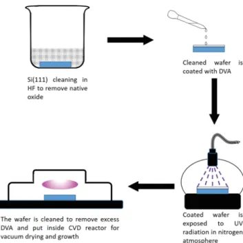
Figure 1. Schematic of the diamond growth with chemical nucleation. The wafers werefirst cleaned with HF to remove native oxide and then subsequently coated with DVA and followed by a multistep growth process.
Table 1. List of Samples
sample DVA lamp
exposure duration (h) incubation duration (min) growth duration (min) S1 yes D 1 30 S2 yes D 1 240 S3 yes D 1 60 S4 yes D 1 5 60 S5 yes D 1 15 60 S6 yes D 1 30 60 S7 yes D 1 45 60 S8 yes D 1 60 60 S9 yes D 1 30 510 S10 yes Xe 24 30 60 S11 yes D 24 30 60 S12 yes 30 60 S13 no 30 60
http://doc.rero.ch
growth temperatures, reducing the thickness of the poorer quality interfacial region26 as required in the growth of thin films. In addition, upon closer inspection of the AFM images it can be seen that there is considerable surface damage for the film with longer exposure to the plasma, and reiterated by the SEM image of the sample shown in Panel C. Such damage on the surface is not visible in the shorter incubation period sample, S1.
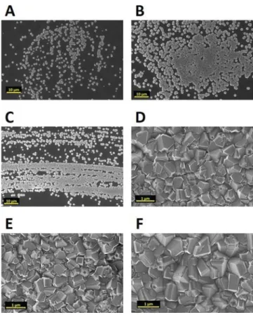
Once it was established that the initial low temperature step of 30 min in duration can give rise to diamond nucleation sites, thickerfilms were grown through varying the incubation time between 0 and 60 min in intervals of 5 min to obtain the minimum time needed to observe coalescedfilms. SEM images of the resulting S3−S8 samples are shown within panels A−F, respectively, ofFigure 3. After the varying-duration, low-plasma density/low-temperature incubation step, the power density of the plasma was increased to raise the substrate temperature to approximately 850°C for a growth duration of 1 h. From the images, it is quite clear that the low-temperature incubation
step plays a crucial role in the growth offilms; as the length of incubation is increased, the number of nucleation sites surviving the high plasma density step increase, giving rise to coalesced films. For the samples grown with incubation periods of 0, 5, and 15 min (panels A, B, and C, respectively), growth leads to island growth partially covering the substrate, whereas the samples incubated for longer than 30 min (panels D, E, and F) shows coalescedfilms as a result of stabilization of the seeds from the DVA solution. Therefore, an incubation step of 30 min at temperatures below 250°C is needed for the nucleation sites to grow large enough to survive the high-plasma-density growth regime. Finally,Figure 4shows afilm with a incubation phase of 30 min that has been subjected to an extended growth period of 510 min. As can be made out, the thickerfilm shows a continuous polycrystallinefilm with large grains.
To test the quality of the resulting films, we studied the samples with considerable coalescence with Raman spectros-copy. Figure 5 shows the resulting Raman measurements of samples S8 and S9. The 1332 cm−1diamond peak is seen in both the samples with little evidence of G-band (1560 cm−1) and D-band (1350 cm−1) peaks attributable to ordered sp2 carbon and amorphous carbon, respectively. For the thinner sample, the second-order TO peak of silicon is also visible at 950 cm−1.
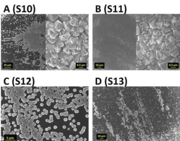
With the demonstration that DVA can lead to enhanced nucleation on Si(111), individual steps were then systematically varied to investigate their importance within the seeding process in samples S10−S13, with the results shown inFigure 6. All the samples were exposed to similar CVD conditions of
Figure 2. Panels A and B show the atomic force microscopy images of samples S1 and S2 produced with incubation periods of 30 and 240 min, respectively. For the 30 min incubation sample within panel A nucleated diamonds are clearly present with an average height of 5 nm, while the 240 min sample shows similar texture with a larger average height of approximately 20 nm. Panel C, meanwhile, shows damage present on the surface of the 240 min sample arising from the plasma.
Figure 3. Scanning electron micrographs of samples S3−S8 (A−F, respectively) produced with 0−60 min of incubation and subsequent hour of growth. At an incubation period of 30 min (panel D), a transition is visible from isolated island growth to coalesced film, indicating an incubation period of at least 30 min is required to produce thinfilms.
30 min under low-density plasma conditions, resulting in substrate temperatures below 250°C, followed by 1 h exposure to high-density plasma conditions with substrate temperatures of approximately 900°C.
To investigate the effect of the wavelength on the grafting process, we used two different radiation sources with different emission spectra. During the earlier study by Giraud et al.,22a Xenon arc lamp was used for 24 h while filtering out wavelengths above 280 nm to minimize heating of the DVA, suggesting wavelengths within the UV are required. Therefore, S10 wasfirst coated with DVA and then exposed to white light for 24 h using a Xe-arc lampfitted with an IR filter to avoid any overheating of the sample. As seen from panel A inFigure 6, it is clear that this process enhances nucleation with a mix of isolated island growth and areas of partial coalescence over the substrate surface. The zoomed-in image of one such island (right-hand side of panel A in Figure 6) clearly shows a continuousfilm. S11 was meanwhile exposed for 24 h to UV
radiation through the use of a deuterium lamp. In this case, the sample presents a higher nucleation density and a more coalescedfilm with less of the substrate being visible. This film is similar to thefilms with just 1 h exposure to UV radiation, as shown within panel D ofFigure 3, indicating saturation of the attachment of the DVA molecule to the silicon surface. The reduced time required to attach DVA to the silicon substrate when using deuterium lamp is believed to be due to the higher intensity of UV radiation emitted in comparison to the xenon lamp.
To see the effects of radiation on the resulting nucleation density, we prepared sample S12 by coating the sample substrate with DVA and leaving in a nitrogen atmosphere for the same duration as S10 and S11 without exposure to radiation. Enhancement in nucleation is clearly visible (panel C in Figure 6) but the absence of coalesced film illustrates the importance of the exposure to UV light. Finally, sample S13 was left untreated with DVA, cleaned with ethanol, DI water, and dicholoromethane, and then placed inside the CVD chamber. As is evident with the low density of crystals visible within panel D ofFigure 6, the DVA coating plays an important role in the nucleation of diamond. Based on the results shown above it can be concluded that the attachment of the DVA molecule to the silicon substrate happens under radiation wavelengths below 250 nm since the Xe lamp used in this experiment radiates between 250 and 950 nm while the deuterium lamp radiates between 160 and 400 nm. Also, the efficiency of attachment while using deuterium lamp is much higher because samples with 1 and 24 h exposure have similar nucleation densities and coverage area. A point that needs to be emphasized here is the deuterium lamp is a 30 W source, whereas the xenon lamp is a 300 W source. Even though the deuterium lamp is one-tenth the power of xenon lamp, we have effective attachment with much less exposure because the component of radiation needed for grafting is more prominent in the deuterium lamp.
So far, the results discussed are based on the use of DVA as chemical precursor, derived from adamantanone using a complex chemical process,28 which in turn is produced when adamantane is dissolved in sulfuric acid.29 To see if it is
Figure 4. Scanning electron micrograph of sample S9 showing produced with an incubation period of 30 min followed by an extended growth duration of 510 min large diamond grains.
Figure 5. Raman spectrum of samples S8, S9, and silicon background diamond peaks in the sample. In both samples the 1332 cm−1 is prominent with little indication of nondiamond carbon through the presence of the G-band or D-band peaks at 1560 and 1350 cm−1, respectively.
Figure 6. SEM images of samples S10−13 produced to investigate the importance of each step of the seeding process are shown in panels A− D, respectively. The tiles to the right of panels A, B, and C show magnified views of the coalesced sections of the respective films.
essential to tailor the adamantane molecule to be effective for chemical nucleation, further experiments with adamantane and 1-mercaptoadamantane(C10H16S) dissolved in cyclohexane were conducted along with studies of the effects of solvents like toluene and cyclohexane on the crystal density through the use of the low temperature incubation step. Furthermore, while previous studies have dissolved tailored diamondoids in solvents such as toluene16it needs to be seen if such chemicals can also give rise to nucleation sites. Four samples were therefore spin- coated with various chemical precursors and then exposed to CVD with the process detailed previously (low temperature incubation for 30 min followed by high temper-ature growth for 60 min). The chemical precursors used were (A) adamantane in cyclohexane, (B) 1-mercaptoadamantane in cyclohexane, (C) cyclohexane, (D) toluene. None of these samples were exposed to any radiation prior to deposition.
Panel A in Figure 7 shows the SEM image of sample spin coated with adamantane dissolved in cyclohexane, with little difference in the density when comparing to the SEM of the untreated sample of Figure 6D. In panel B, meanwhile, the SEM image of the sample which was spin coated with 1-mercaptoadamantane dissolved in cyclohexane is shown with a clear enhancement in nucleation. This is a clear indication that
to use adamantane for chemical nucleation it is important to tailor the parent molecule to enhance the attachment to the substrate surface.
Lastly, the effects of solvents like toluene, cyclohexane, and dicholoromethane were also examined. Although it is possible to remove the effects of dichloromethane completely (Figure 6D), the same is not the case for cyclohexane or toluene. Even after extensive cleaning, samples coated with cyclohexane or toluene showed enhanced nucleation as seen in the SEM images in panels C and D ofFigure 7, respectively. In the case of toluene the enhancement was more pronounced with the presence of diamond microislands. It should be noted that the low-temperature step of the growth at 250°C is well above the boiling point of toluene. In the last two panels of Figure 7, zoomed-in views of sections from panel D are shown with panel E showing a magnified view of one of the numerous nanodiamonds, whereas panel F shows a magnified view of the area marked by the yellow box. From the magnified views, clear faceting of the surfaces can be seen, confirming the high quality of the diamond nanoparticles, whereas the coalesced area is reminiscent of NCD films. Such continuous areas may be possible because of the low-temperature step introduced in our process but it is the chemical nucleation using DVA that is capable of giving coalesced films over large areas, not just microislands. In combination with the previous reports on the increase in nucleation upon using organic precursors as reported within the introduction, it is clear from the present studies that solvent choice is therefore important when coating the substrates with tailored adamantane molecules.
4. CONCLUSION
A modified adamantane molecule (DVA) has been used to create nucleation sites on nondiamond substrates for the growth of thin diamondfilms. Tethering of the modified DVA molecule through the UV-driven homolysis of the Si−H bonds present on the substrate has been demonstrated to minimize the effect of sublimation, allowing the molecules to act as nucleation sites. A low-temperature incubation step of 250°C allowing the seeds to stabilize and subsequent conventional growth regime at 850 °C has then been shown to produce highly coalesced and high-quality diamond thinfilms. It has also been demonstrated that the choice of adamantane-containing solvent can give rise to nucleation sites, necessitating careful removal of all traces before subjecting the treated substrates to CVD.
■
AUTHOR INFORMATIONCorresponding Authors
*E-mail:mandals2@cardiff.ac.uk. *E-mail:williamso@cardiff.ac.uk.
Notes
The authors declare no competingfinancial interest.
■
ACKNOWLEDGMENTSThis project is supported by Engineering and Physical Sciences Research Council, UK, Grant EP/K007459/1.
■
REFERENCES(1) Ohtsuka, K.; Suzuki, K.; Sawabe, A.; Inuzuka, T. Epitaxial Growth of Diamond on Iridium. Jpn. J. Appl. Phys. 1996, 35, L1072−L1074.
(2) Verstraete, M. J.; Charlier, J.-C. Why is Iridium the Best Substrate for Single Crystal Diamond Growth? Appl. Phys. Lett. 2005, 86, 191917.
Figure 7. SEM images of samples grown to see the effect of tailoring the adamantane molecule as well as the effect various solvents have on nucleation. (A) Image of the sample that was spin-coated with adamantane dissolved in cyclohexane. In this case, no enhancement in nucleation is observed. (B) Enhanced nucleation observed on silicon pieces spin coated with 1-mercaptoadamantane dissolved in cyclo-hexane. (C) Image of diamond particle growth on samples washed with cyclohexane. Even though the sample is sparsely covered, the density is higher than that seen on untreated silicon pieces. (D) Islands of diamond grown on silicon treated with toluene. (E) Image of one of the many clearly faceted diamond nanoparticle seen on samples treated with toluene as seen in panel D. (F) Magnified view of the sample in the yellow box of panel D.
(3) Jiang, X.; Schiffmann, K.; Westphal, A.; Klages, C. Atom-icForceMicroscopic Study of Heteroepitaxial Diamond Nucleation on (100) Silicon. Appl. Phys. Lett. 1993, 63, 1203−1205.
(4) Williams, O. A. Nanocrystalline Diamond. Diamond Relat. Mater. 2011, 20, 621−640.
(5) Spitsyn, B.; Bouilov, L.; Derjaguin, B. Vapor Growth of Diamond on Diamond and Other Surfaces. J. Cryst. Growth 1981, 52, 219−226. (6) Suzuki, K.; Sawabe, A.; Yasuda, H.; Inuzuka, T. Growth of Diamond Thin Films by dc Plasma Chemical Vapor Deposition. Appl. Phys. Lett. 1987, 50, 728−729.
(7) Ravi, K. V.; Koch, C. A.; Hu, H. S.; Joshi, A. The Nucleation and Morphology of Diamond Crystals and Films Synthesized by the Combustion Flame Technique. J. Mater. Res. 1990, 5, 2356−2366.
(8) Iijima, S.; Aikawa, Y.; Baba, K. Early Formation of Chemical Vapor Deposition Diamond Films. Appl. Phys. Lett. 1990, 57, 2646− 2648.
(9) Ascarelli, P.; Fontana, S. Dissimilar Grit-Size Dependence of the Diamond Nucleation Density on Substrate Surface Pretreatments. Appl. Surf. Sci. 1993, 64, 307−311.
(10) Yugo, S.; Kimura, T.; Muto, T. Effects of Electric Field on the Growth of Diamond by Microwave Plasma {CVD}. Vacuum 1990, 41, 1364−1367.
(11) Williams, O. A.; Douhéret, O.; Daenen, M.; Haenen, K.; Osawa, E.; Takahashi, M. Enhanced Diamond Nucleation on Monodispersed Nanocrystalline Diamond. Chem. Phys. Lett. 2007, 445, 255−258.
(12) Tiwari, R. N.; Chang, L. Growth, Microstructure, and Field-Emission Properties of Synthesized Diamond Film on Adamantane-coated Silicon Substrate by Microwave Plasma Chemical Vapor Deposition. J. Appl. Phys. 2010, 107, 103305.
(13) Tsugawa, K.; Ishihara, M.; Kim, J.; Koga, Y.; Hasegawa, M. Nucleation Enhancement of Nanocrystalline Diamond Growth at Low Substrate Temperatures by Adamantane Seeding. J. Phys. Chem. C 2010, 114, 3822−3824.
(14) Tiwari, R. N.; Tiwari, J. N.; Chang, L.; Yoshimura, M. Enhanced Nucleation and Growth of Diamond Film on Si by CVD Using a Chemical Precursor. J. Phys. Chem. C 2011, 115, 16063−16073.
(15) Chen, Y.-C.; Chang, L. Chemical Vapor Deposition of Diamond on Silicon Substrates Coated with Adamantane in Glycol Chemical Solutions. RSC Adv. 2013, 3, 1514−1518.
(16) Zhang, J. L.; et al. Hybrid Group IV Nanophotonic Structures Incorporating Diamond Silicon-Vacancy Color Centers. Nano Lett. 2016, 16, 212−217.
(17) Lee, S. T.; Peng, H. Y.; Zhou, X. T.; Wang, N.; Lee, C. S.; Bello, I.; Lifshitz, Y. A Nucleation Site and Mechanism Leading to Epitaxial Growth of Diamond Films. Science 2000, 287, 104−106.
(18) Olah, G. In Cage Hydrocarbons; Olah, G., Schleyer, P. V., Eds.; Wiley: New York, 1990; pp 1−45.
(19) Linford, M. R.; Chidsey, C. E. D. Alkyl Monolayers Covalently Bonded to Silicon Surfaces. J. Am. Chem. Soc. 1993, 115, 12631− 12632.
(20) Linford, M. R.; Fenter, P.; Eisenberger, P. M.; Chidsey, C. E. D. Alkyl Monolayers on Silicon Prepared from 1-Alkenes and Hydrogen-Terminated Silicon. J. Am. Chem. Soc. 1995, 117, 3145−3155.
(21) Leroy, E.; Küttel, O. M.; Schlapbach, L.; Giraud, L.; Jenny, T. Chemical Vapor Deposition of Diamond Growth Using a Chemical Precursor. Appl. Phys. Lett. 1998, 73, 1050−1052.
(22) Giraud, A.; Jenny, T.; Leroy, E.; Küttel, O. M.; Schlapbach, L.; Vanelle, P.; Giraud, L. Chemical Nucleation for CVD Diamond Growth. J. Am. Chem. Soc. 2001, 123, 2271−2274.
(23) Pehrsson, P. E.; Morrish, A. A. Hydrocarbon Oil-Based Acceleration of CVD-Diamond Nucleation. In Proceedings of the 2nd International Conference on New Diamond Science and Technology; Washington, D.C., Sept 23−27, 1990 Materials Research Society: Pittsburgh, PA, 1991; pp 397−402.
(24) Ece, M.; Oral, B.; Patscheider, J.; Ernst, K.-H. Effect of Organic Precursors on Diamond Nucleation on Silicon. Diamond Relat. Mater. 1995, 4, 720−724.
(25) Bevan, W. I.; Haszeldine, R. N.; Middleton, J.; Tipping, A. E. Polyfluoroalkyl Compounds of Silicon. Part XII. Reactions of
Trichlorosilane with 2-chloro- and 2-bromo-1,1-difluoroethylene. J. Chem. Soc., Dalton Trans. 1974, 2305−2309.
(26) Williams, O. Nanocrystalline Diamond. Diamond Relat. Mater. 2011, 20, 621−640.
(27) Arnault, J.; Saada, S.; Nesladek, M.; Williams, O.; Haenen, K.; Bergonzo, P.; Osawa, E. Diamond Nanoseeding on Silicon: Stability Under {H2} {MPCVD} Exposures and Early Stages of Growth. Diamond Relat. Mater. 2008, 17, 1143−1149.
(28) Giraud, L.; Huber, V.; Jenny, T. 2,2-Divinyladamantane: A New Substrate for the Modification of Silicon Surfaces. Tetrahedron 1998, 54, 11899−11906.
(29) Geluk, H.; Schlatmann, J. Hydride Transfer Reactions of the Adamantyl CationI. Tetrahedron 1968, 24, 5361−5368.