HAL Id: tel-01726290
https://tel.archives-ouvertes.fr/tel-01726290
Submitted on 8 Mar 2018HAL is a multi-disciplinary open access archive for the deposit and dissemination of sci-entific research documents, whether they are pub-lished or not. The documents may come from teaching and research institutions in France or abroad, or from public or private research centers.
L’archive ouverte pluridisciplinaire HAL, est destinée au dépôt et à la diffusion de documents scientifiques de niveau recherche, publiés ou non, émanant des établissements d’enseignement et de recherche français ou étrangers, des laboratoires publics ou privés.
Area Evaluation for 14nm and beyond
Alexandre Ayres de Sousa
To cite this version:
Alexandre Ayres de Sousa. 3D Monolithic Integration : performance, Power and Area Evaluation for 14nm and beyond. Micro and nanotechnologies/Microelectronics. Université Grenoble Alpes, 2017. English. �NNT : 2017GREAT065�. �tel-01726290�
Pour obtenir le grade de
DOCTEUR DE LA COMMUNAUTE UNIVERSITE
GRENOBLE ALPES
Spécialité : Nano Electronique et Nano Technologies
Arrêté ministériel : 25 mai 2016
Présentée par
Alexandre AYRES DE SOUSA
Thèse dirigée par Laurent FESQUET et
co-encadrée par Olivier ROZEAU et Bertrand BOROT
préparée au sein du Laboratoire Techniques de l'Informatique et de la
Microélectronique pour l'Architecture des systèmes intégrés (TIMA) et du Laboratoire d'électronique des technologies de l'information (CEA-LETI)
au sein de l'École Doctorale électronique, électrotechnique, automatique et
traitement du signal (EEATS)
Intégration monolithique en 3D: étude du
potentiel en termes de consommation,
performance et surface pour le nœud
technologique 14nm et au-delà
Thèse soutenue publiquement le 16 Octobre 2017, devant le jury composé de :
Pr. Francis CALMON
Professeur des Universités,INSA de Lyon, Lyon (Président)
Pr. Lionel TORRES
Professeur des Universités, université de Montpellier, Montpellier (Rapporteur)
Dr. Olivier ROSSETTO
Maître de conférences, université Grenoble Alpes, Grenoble (Membre)
Dr. Laurent FESQUET
Maître de conférences, Grenoble INP, Grenoble, (Directeur de thèse)
Dr. Olivier ROZEAU
Ingénieur de recherche au CEA-Leti, Grenoble (Membre Invité)
Mr. Bertrand BOROT
ACKNOWLEDGMENTS
My doctoral thesis took place between 2014 and 2017 in Grenoble, France. It was performed in collaboration among STMicroelectronics in Crolles, the research institute of the French Alternatives Energies and Atomic Energy Commission (CEA-LETI) in Grenoble and the TIMA laboratory from Grenoble-Institute of Technology (Grenoble INP). This environment including enterprise, research institute and academia allowed me to be in the center of the Grenoble semiconductor development “war machine”. The level of excellence and competence in the Grenoble ecosystem inspired me.
I would like to thank all people who gave me this fantastic and unique opportunity, and welcomed a Brazilian that had just left the electrical engineering school. In a great surprise I have met nice, intelligent and welcoming people 9000 km away from home. The adventure of coming to France without even knowing the basics in the French language, quickly turned in a pleasant life, in a lovely country. As a CIFRE thesis program, I could experience the importance of academia close to the industry.
The TIMA laboratory and its team amused me by their competence in semiconductor design. I would like to thank the whole team which I had the opportunity to discuss my work several times and receive constructive feedback. A warmhearted thanks to all Brazilian friends working at TIMA to whom I wish the best. I specially thank Rodrigo BASTOS. I had the luck to work with Laurent FESQUET, who gave me an incredible guidance, quickly solved my problems with tight deadlines, always with clear insights and gently. At STMicroelectronics, my gratitude to Bertrand BOROT, his competence, readiness, technical knowledge and management will be inspiration for the rest of my days. I greatly appreciate the Crolles fast pace, the industrial environment and support for new ideas.
I spent most of my PhD at the LICL laboratory from CEA-LETI. I have gained a lot of advanced process technical knowledge at LETI, even working with design. My gratitude to Louis HUTIN, Perrine BATUDE, François ANDRIEU, Laurent BRUNET and Claire FENOUILLET who were always prompt to discuss and explain ideas. Also, a big thanks to Olivier ROZEAU. I could write a book of the adventures of being advised by Olivier. His excellence, attention to the details, competence and rigor always pushed me to move forward. I am really honored to have worked with him. I also particularly thank Mathilde, Julien, Luca, Lina, José, Julien, Jessy, Remy, Fabien, Vincent and Giulia for the great times spent during my thesis. Really nice people, to whose I wish the best. I can speak French now because the insistence of Julien, Mathilde and Lina who always taught me.
Finally, my deepest gratitude to my family who have supported me unconditionally. Despite of the distance and seeing them only few days per year, I always felt their support which kept me strong in the difficult times. A genuine thanks to my parents Alexandre and Adriene.
Sincerely,
TABLE OF CONTENTS
TABLE OF CONTENTS ... 5
GLOSSARY ... 8
1 CHAPTER ONE – INTRODUCTION TO 3DVLSI ... 12
1.1 INTRODUCTION TO 3DVLSI ... 13
1.1.1 CMOSSCALING ... 13
1.1.2 MOSFETDEVICE OVERVIEW AND TYPICAL FIGURES OF MERIT ... 16
1.1.3 DENNARD’S SCALING ... 19
1.1.4 2000’S TECHNICAL ADVANCES ON SCALING ... 21
1.1.5 RISE OF NEW MOSFET ARCHITECTURES ... 23
1.2 3DINTEGRATION AS MORE THAN MOORE’S ALTERNATIVE ... 28
1.2.1 MOTIVATION AND CONCEPT ... 28
1.2.2 TSV–PARALLEL INTEGRATION ... 30
1.2.3 MONOLITHIC 3DSEQUENTIAL INTEGRATION –STATE OF THE ART ... 33
1.3 THESIS OBJECTIVES ... 40
1.4 CHAPTER CONCLUSION ... 41
PART ONE: DESIGN ... 46
2 CHAPTER TWO – TRANSISTOR LEVEL 3D DESIGN ... 48
2.1 VLSIDIGITAL DESIGN FLOW ... 49
2.1.1 OVERVIEW IN PLANAR DESIGN FLOW ... 49
2.1.2 3DDESIGN FLOW ... 50
2.1.3 DESIGN FLOW WITH EDA ... 51
2.1.4 CONCLUSION AND POSITIONING ... 53
2.2 BOTTOM-UP APPROACH FOR THE DIGITAL DESIGN FLOW ... 54
2.2.1 FULL CUSTOM STANDARD CELL ... 54
2.3 3DDESIGN ENVIRONMENT ... 60
2.3.1 MOSFETPERFORMANCE AND SPICEMODELS ... 60
2.3.2 SIMULATION RESULTS ... 60
2.3.3 PARASITIC ELEMENTS EXTRACTIONS ... 61
2.3.4 CONCLUSION ... 61
2.4 ELECTRICAL DESIGN CHARACTERIZATION ... 62
3 CHAPTER THREE – BEOL PROCESS INFLUENCE ON 3D DESIGN ... 77
3.1 GUIDELINES ON 3DVLSIBEOL PROCESS DEVELOPMENT ... 78
3.1.1 IBEOLLIMITATIONS ... 78
3.1.2 IBEOL FLAVORS AND RING OSCILLATORS ... 79
3.2 BEOLLIMITATIONS IN ADVANCED NODES ... 85
3.2.1 SCALING EXPECTATIONS ... 85
3.2.2 WIRELENGTH DELAY IN ADVANCED NODES ... 86
3.3 CHAPTER CONCLUSION ... 90
PART TWO: VARIABILITY ... 92
4 CHAPTER FOUR – VARIABILITY IN VLSI ... 94
4.1 VARIABILITY IN VLSICIRCUITS ... 95
4.1.1 SOURCES OF PROCESS VARIABILITY ... 95
4.1.2 PELGROM’S VARIABILITY –LOCAL VARIATIONS ... 95
4.1.3 GLOBAL VARIABILITY ... 98
4.1.4 ACV ... 99
4.1.5 MONTE CARLO ANALYSIS ... 101
4.1.6 PROCESS CORNERS MANAGEMENT ... 102
4.2 SPICEMODEL STATISTICAL EVALUATION ... 103
4.2.1 STATISTICAL INPUTS ... 103
4.2.2 PARAMETER SENSITIVITY ... 106
4.3 CHAPTER CONCLUSION ... 108
5 CHAPTER FIVE – VARIABILITY EFFECTS IN 3DVLSI DESIGN ... 113
5.1 GLOBAL AND LOCAL EFFECTS IN RING OSCILLATORS AND SRAMS ... 114
5.1.1 PLANAR BEHAVIOR ... 114
5.1.2 3DPARTITIONING EFFECTS ... 117
5.2 STATISTICAL UNIFIED MODEL ... 123
5.2.1 MODEL DEFINITIONS ... 123
5.2.2 RING OSCILLATORS SENSIBILITY TO DIFFERENT SOURCES ... 126
5.2.3 3DPARTITIONED SRAMVARIABILITY ... 128
5.2.4 SRAMSTATIC NOISE MARGIN ... 130
5.2.5 SRAMSTATIC POWER ... 133
5.3 CHAPTER CONCLUSION ... 134
6 CHAPTER SIX – CONCLUSION ... 136
6.1.2 THE 3D OPPORTUNITY ... 137
6.1.3 ADVANTAGES OF 3D DESIGN FOR VARIABILITY ... 138
6.2 GENERAL CONCLUSION ... 140
6.3 PROSPECTS ... 141
6.3.1 CMOS LOGIC INTEGRATION AND MEMORIES –SEVERAL TIERS SCALING ... 141
6.3.2 MORE THAN LOGIC –FUNCTIONALITY INTEGRATED SEQUENTIALLY ... 141
A. APPENDIX A ... 143
A.1THESIS TOOLS CONTEXT ... 144
A.1.1 A.1.13DDESIGN ENVIRONMENT ... 144
A.1.2 FULL CUSTOM VS STANDARD CELL INTEGRATION ... 145
B. APPENDIX B ... 147
B.1 SRAMSIGNAL NOISE MARGIN (SNM)SIMULATIONS ... 148
B.1.1 SRAMSPICENETLIST ... 148
B.1.3 CORRELATION TREATMENT IN THE NETLIST ... 152
TITLE: 3D MONOLITHIC INTEGRATION: PERFORMANCE, POWER AND AREA EVALUATION FOR 14NM AND BEYOND ... 156
TITRE: INTEGRATION MONOLITHIQUE EN 3D: ETUDE DU POTENTIEL EN TERMES DE CONSOMMATION, PERFORMANCE ET SURFACE POUR LE NŒUD TECHNOLOGIQUE 14NM ET AU-DELA ... 156
Acronyms
Meaning
3DCO 3D Monolithic Contact Between Tiers 3DVLSI Very-Large-Scale 3D Monolithic Integration ACV Across-Chip Variations
ASIC Application-Specific Integrated Circuit
BEOL Back-End Of Line
BOX Buried Oxide
CMOS Complementary Metal-Oxide-Semiconductor CMP Chemical Mechanical Planarization
CPP Contacted Poly Pitch DES Data Encryption Standard DIBL Drain-Induced Barrier Lowering
DRC Design Rules Check
DRM Design Rules Manual
EDA Electronic Design Automation EOT Equivalent Oxide Thickness EUV Extreme Ultra-Violet
FD-SOI Fully Depleted Silicon On Insulator
FEOL Front-End Of Line
FF Flip-Flop
FFT Fast-Fourier Transform FinFET Fin Field Effect Transistor
FO Fan-Out
GAA Gate-All-Around
GND Ground
GPU Graphic Processor Unit
High-k Relative permittivity higher than SiO2
HUEBR Heated Unique and Equal Bonding Reliability iBEOL Intermediate Back-End Of Line
IV Inverter Gate
LDPC Low-Density Parity-Check LIDAR Light Detection and Ranging
LoL Logic over Logic
LT Low Temperature Process
LVS Layout Versus Schematic
MC Monte Carlo
MDR Metal Design Routing
MOSFET Metal-Oxide-Semiconductor Field Effect Transistor Mx Metal Layer Level - M1 standards for layer one
NMOS Metal-Oxide-Semiconductor with an n-type conduction channel PAI Pre-amorphization-Assisted Implantation
PDK Process Design Kit PDN Power Delivery Network
PD-SOI Partially-Depleted Silicon On Insulator PEX Parasitic Extraction
PMOS Metal-Oxide-Semiconductor with an p-type conduction channel PPA Performance, Power and Area Metric
RF Radio Frequency
RO Ring Oscillator
RSD Raised Source-Drain RSNM Read Static Noise Margin RTL Register-Transfer Level RX Transistor Active Region
S/D Source and Drain
SNM Static Noise Margin SOI Silicon On Insulator
SPER Solid-Phase Epitaxial Regrowth
SPICE Simulation Program with Integrated Circuit Emphasis SRAM Static Random-Access Memory
SS Subthreshold Swing
STR Self-Timed Ring
TSV Through-Silicon Via UTBOX Ultra-Thin Buried Oxide VDD Positive Supply Voltage VLSI Very-Large-Scale Integration VTC Voltage Transfer Characteristics
WL Wirelength
WNM Write Noise Margin
INTRODUCTION TO CHAPTER ONE
“There's a basic principle about consumer electronics: it gets more powerful all the time and it gets cheaper all the time.” --Trip Hawkins
The integrated circuit evolution over the years has changed the world. From massive data centers to mobile devices, the electronic is in our life.
Chapter one discusses how the above quote is possible. The historical perspective of making smaller devices, namely the transistor scaling is reviewed by discussing the Moore’s Law. Over the last 50 years the scaling trend has been achieved, decreasing the costs per transistor.
The MOSFET transistor operation and its figure of merits are briefly discussed. The MOS is the fundamental brick in the digital nanoelectronics, and increasing its performance translate in a better circuit efficiency. Quantifying transistor characteristics for digital operation is necessary to determine the best circuit behavior.
Dennard’s Law is an insight into the transistor performance boost by the miniaturization. By scaling parameters such as widths, lengths, thickness the transistor performance is enhanced. Coupled to Moore’s Law, the outcome is the cited quote.
The 3D integration concept and state of the art is shown in this chapter. As the scaling is approaching to the atomic level size, the process complexity is escalating. The 3D integration, or stacking transistor in several tiers is presented as an alternative to the traditional scaling. The parallel 3D integration is briefly discussed, and then the state of the art of 3D sequential is reviewed.
1.1 Introduction to 3DVLSI
1.1.1 CMOS Scaling
In the 1960’s electronic circuits suffered a major transformation, the circuitries were in a transition from discrete elements to fully integration on a single die. Gordon Moore noted that the number of transistor was increasing year by year, and possibly the trend could continue through the following years, as no fundamental physical barrier was in sight. The trend was first proposed for the next ten years, or until 1975 as illustrated in Figure 1.1.1.1a.
Figure 1.1.1.1 “Cramming more components onto integrated circuits”. On the left, (a) Moore’s transistor count projection through the years. On the right, (b) the optimum number of components to decrease the cost. During the years the optimum cost is reduced and the optimum transistor count is higher. [Moore 1998].
In the same publication, Moore argues that the cost of the circuit is inversely proportional to the number of components. This holds true until a certain point, where the huge number of components increment the circuit complexity and reduces the process yield, thus increases the cost. The outcome is an optimum number of components for the minimum cost. Moore’s then predicts the cost failing over the years, especially for the optimum number of components in an integrated circuit as illustrated in Figure 1.1.1.1b. Miniaturization and technology evolution are cited as the main reason to reducing costs. The main messages of the paper are the beginning of a new era using integrated circuit, instead of the previous discrete circuits; the benefits of using integrated circuits, such as reliability, increased circuit complexity and utility, and most importantly the cost reduction proportioned by the miniaturization. Those arguments form the base of the well-known Moore’s law: over the years the cost per transistor is reduced, because the advancements in the technology and miniaturization. The original paper cites the miniaturization pace of doubling the transistor count every two years, thus the transistor count in Figure 1.1.1.1a is in the logarithm scale. Another interesting discussion in the publication is the process yield, which is said to improve as high as economically possible, only needing engineering efforts. This confirms the central key
Moore had only data from the previous six years, and made the prediction of transistor count for the next ten years, or until 1975. It turns out, that the proposed miniaturization pace proposed by Moore held true for at least 52 years. The scaling of transistors is occurring for five decades, and the transistor count should increase in the next years, continuing the Moore’s scaling trend. After many years of success, the Moore`s prediction became more than a classic paper, it turned into a law. Indeed, the transistor count doubling each eighteen or twenty-four months is the big roadmap followed by the industry, especially for the advanced logic integration. The transistor dimension scaling has been scaled as shown in Figure 1.1.1.2, often depicted as the Moore’s Law. Despite of transistor count being the imminent result of the scaling, the reason that Moore’s Law is alive after so many years is the transistor cost, as proposed in the original paper. The cost per transistor is decreasing for each node, as pictured in Intel data in Figure 1.1.1.3. As suggested by Moore, this figure shows that more transistors can be crammed for a given area, and despite the cost increasing in each node due to process complexity, the final price per transistor is decreasing. This trend is expected to continue at the 7nm node by Intel. A major caveat in the data is about the yield and process maturity. Those factors are not transparent, so the analysis may consider a very good process yield and the cost per transistor after a long time of mass production, where the process maturity is good enough to deliver high yields, and optimized performance.
Figure 1.1.1.3 Intel data for the relative transistor cost from the 130nm to 7nm node. The cost per transistor is decreasing in a logarithm scale.
1.1.2 MOSFET Device Overview and Typical Figures of Merit
The Metal-Oxide-Semiconductor Field Effect Transistor abbreviated by MOSFET is the structure created using the three elements (MOS) as the name suggests, in order to create a layer of free carriers by applying of electrical field in the semiconductor. The transistor has four terminals, the gate which controls the semiconductor channel, the source and drain, and finally a body terminal connecting the semiconductor mass. As consequence, the field is able to control the current density of these free carriers, either electrons or holes, effectively changing the semiconductor conductivity between the drain and the source. The semiconductor can be classified as N-type or P-type depending on the majority of electric carriers. The source and drain are doped regions accordingly to the MOSFET type (NMOS or PMOS) and opposite to the channel type, forming a NPN or PNP structure respectively. The typical bulk structure is illustrated in Figure 1.1.2.1a as well the contacts in Figure 1.1.2.1b FD-SOI MOSFET transistor. In schematic abstraction level, the NMOS is represented as Figure 1.1.2.1c.
Figure 1.1.2.1 (a) Typical Bulk MOSFET; (b) FD-SOI MOSFET with 4 terminals; (c) Schematic representation of NMOS.
The gate field effect can modulate the charge concentration in the channel region, this effect is possible due to the MOS capacitance structure. For a NMOS, when gate voltage bias is applied, after a certain level (called threshold voltage) it can create an inversion layer in the P-substrate, meaning that substrate-gate oxide interface is populated with electrons, and then an electrical current can flow from drain to source. In an ideal condition, no current flows when the gate bias is under the threshold voltage. In real devices, a small current can flow even if the gate is turned off, and this effect is called leakage current. The leakage arises from the junction’s carrier recombination as well as the tunneling effects, such as gate-oxide leakage [J. Chen 1987]. The bulk terminal can modulate the voltage across the semiconductor substrate, modifying the channel charges concentration, thus providing a VT shift in order to decrease the leakage or
increase the performance. The typical MOSFET top-view for design layout is shown in Figure 1.1.2.2. The active region, or the complete transistor bulk is seen in green. The gate stack is simplified as strip shown in red. The source and drain contacts are in white and blue. This is a typical representation for planar transistor, either bulk or FDSOI. With FinFETs the design layout may differ, as the Fins are shown in the layout, and the bulk region may not be represented. The gate length LG was the smallest feature size in
the transistor, and historically was used to name the transistor node, despite of this not holding true anymore.
Figure 1.1.2.2 Simplified top view of transistor layout for (a) Bulk and FDSOI; (b) FinFET
The operation of MOSFET transistor depends on the combination of voltages applied in its four terminals and the analysis is done regarding the current between the drain to source, referenced as ID. In a general
manner, the MOSFET can operate in analog, radio-frequency (RF) and digital domains. The following figures of merit will focus on the digital operation, which the main goal is to switch between the logic states.
Figure 1.1.2.3 (a) Transistor ID current versus gate voltage for 14nm FDSOI; (b) 10nm FinFET for SRAM figures of merit for ID in logarithm scale [S. Y. Wu 2016].
The classic benchmarking parameters are illustrated in Figure 1.1.2.3b by plotting the logarithm ID versus
the gate voltage, in this case for PMOS and NMOS. The parameters are the IOFF, ID SAT, ID LIN, Subthreshold
difference of the threshold voltage for a given delta in VDD. The inverse of the slope of the ID curve is called SS, and it is given by (1.2).
𝐷𝐼𝐵𝐿 =
𝛥𝑉
𝑇𝛥𝑉
𝐷𝐷 (1.1)𝑆𝑆 =
𝜕𝑉
𝐺𝑆𝜕𝑙𝑜𝑔𝐼
𝐷 (1.2)The SS has a minimum value of 60mV/dec for a conventional silicon device, using T=300K and COX >>CDEP,
where COX is the gate-oxide capacitance andCDEP is the depletion layer capacitance. The DIBL is due to the
short channel effect, where the S/D (source and drain) junctions create a superposed depletion laterally under the channel, thus reducing the gate electrostatic control and lowering the transistor VT. By applying
a bias in the drain, this effect is enhanced, thus there is an ID curve difference between the linear and
saturation modes. The DIBL is calculated by the difference of VTSAT and VTLIN. Besides the MOSFET figures of
merit, the final circuit is often evaluated using the Performance, Power and Area (PPA) metric. The first two are directly linked to costumer usability, in the sense of speed, mobility for battery powered devices, emitted heat and power consumption cost. The area is inherently tied to the device cost.
1.1.3 Dennard’s Scaling
Moore’s scaling became a de facto standard in the industry over the years, and it was marketed as the node number metric, representing the transistor minimum feature size, or the gate length. This trend is shown in Figure 1.1.3.1. Starting at 0.25 µm node, the transistor gate length does not represent anymore the real gate size, but due to marketing reasons, the expected node scaling x0.7 trend was kept in the node name.
Figure 1.1.3.1 Transistor gate length feature size over the years. On the left, (a) Intel data and transistor cost [Thompson 2004]; (b) Applied Materials data extrapolation to 2020.
Besides the gate length scaling, the transistor parameters were also being scaled. This overall scaling trend was noted by Robert H. Dennard in 1974 as follows in Figure 1.1.3.2 [Dennard 1974], proposing a performance increase due to scaling. The parameters are scaled by a factor κ.
Figure 1.1.3.2 Dennard’s Scaling parameters to increase circuit performance. [Dennard 1999]
Dennard’s law supposes a constant power density for a given area, thus the voltage and current are scaled by a factor κ-1 while area of a given device is reduced by a factor κ 2. The area reduction for a given element,
such as metal interconnection, is also κ 2 while the dielectric insulating distance decreases by a factor κ,
hence resulting in parasitic capacitance reduction by a factor κ-1. Circuit performance wise, the Moore’s
Scaling is highly beneficial. As noted by Dennard, the several scaling parameters increase the device performance as illustrated in Figure 1.1.3.3 for scaling the spacing between adjacent gates (also defined
circuit performance. In other words, doing more powerful devices made them cheaper. This is sometimes referred as the “scaling free lunch” or “golden age of scaling”. The outcome is strongly opposed to conventional product engineering: usually to make something better, it becomes more expensive.
Figure 1.1.3.3 Performance increase over the years (reducing gate delay). At the same time, the switching power was reduced. [Gargini 2017]
1.1.4 2000’s Technical Advances on Scaling
The scaling met some difficulties to deliver the expected circuit performance in the years 2000’s. New device solutions were proposed and implemented, increasing the process complexity rather than a simple parameter scaling as in the previous years. A brief of major technical solutions is presented in this section.
Figure 1.1.4.1 In the 90nm node, the channel mechanical strain was introduced to increase the transistor performance. [Thompson 2004, 90-].
In the 90nm node, circa 2004, for the first time the devices featured the mechanical strain engineering. The strained silicon is achieved in PMOS by using SiGe in S/D, hence the mismatch between the SiGe and the Si in the channel creates a compressive stress in the P channel improving the hole mobility. In the NMOS channel the tension stress is necessary, thus in Intel process it was achieved by using a high stress nitride-capping layer as in Figure 1.1.4.1. The tensile stress in N channel increases the electron mobility.
Figure 1.1.4.2 In the 45nm node, the gate-oxide was changed from the typical SiO2 to HfO2 High-K isolation. [Mistry 2007]
thickness was reduced over the years in order to increase the Cox, and consequently the transistor performance. However, the thickness required in the 45nm would be lower than 2nm following the scaling trend, and consequently the device would become too leaky, because of the carrier tunneling through the very thin gate oxide. The solution was to use a higher permittivity material than SiO2 (ɛ=3.9). The HfO2 was
chosen, with ɛ>10, allowing a higher Cox, while being thicker than the equivalent SiO2 film, hence reducing
the gate leakage by 25x [Mistry 2007]. After this technology, the Equivalent Oxide Thickness (EOT) definition was widely adopted. It straightforwardly compares a given high-k to SiO2 theoretical thickness
to achieve the same capacitance. The EOT definition is described in 1.3.
Along with gate-oxide change in the 45nm node, some processes started using a gate-last integration in the 22nm node. In this process flow the gate high-k is deposited after the removal of dummy gates and before the metal gate electrodes. This integration avoids the thermal stress in the gate oxide during the S/D annealing. Another solution used in the 2000’s is the raised source and drain (RSD) starting from the 90nm node. This solution reduces the source and drain contact resistance by increasing the contact height, decreasing the S/D sheet resistance, which is in series with the channel resistance, thus increasing the transistor performance. Several process solutions can achieve the raised S/D, for example the selective epitaxial growth [H.-J. Huang 2001].
𝐸𝑂𝑇 = 𝑡ℎ𝑖𝑐𝑘𝑛𝑒𝑠𝑠
𝐻𝑖𝑔ℎ𝐾ɛ
𝑆𝑖𝑂21.1.5 Rise of new MOSFET architectures
After the 28nm node, the standard bulk transistor was difficult to scale even using the improved process developed in the 2000’s. Emergent transistor architectures were employed, and are currently in research. Those architectures are focused on improving the gate electrostatic control over the channel. The industry has been biased over three major architectures illustrated in Figure 1.1.5.1, namely the FD-SOI, FinFETs and Nanowires.
FD-SOI stands for Fully Depleted Silicon On Insulator, and was a technological substrate process evolution from PD-SOI (Partially Depleted version). The Buried Oxide (BOX) limits the bulk leakage, and the S/D extends to BOX, minimizing junction area, leakages as well as the capacitances [Cristoloveanu 1999]. The PD-SOI silicon film thickness (TSI) over the BOX forming the channel is not thin enough to create a depletion
charge fully controlled by the gate as illustrated in Figure 1.1.5.2a. In fact, a quasi-neutral zone is present under the formed channel, and if the body connection is floating some undesirable effects may occur, such as the kink effect (causing hysteresis in ID-VG curves, and potentially latching-up the transistor). Employing
a thin TSI can suppress those undesirable effects because the channel becomes fully depleted 1.3as shown
in Figure 1.1.5.2b. The channel can be controlled by the usual gate, but also from the potential under the BOX, namely the back-gate. The FD-SOI advantages over BULK and PD-SOI are the lower leakage, no latch-up risk, and the lower variability due to lower doping in the channel, as well the increased electrostatic control.
Figure 1.1.5.1 Conceptual transistor archichetures in burried oxide for: (a) FD-SOI; (b) FinFET; (c) Nanowires.
Figure 1.1.5.2 (a) PD-SOI concept; (b) FD-SOI concept; (c) FD-SOI TEM cross section image [Weber 2010].
A TSI of 6nm is shown in Figure 1.1.5.2c for a 28nm FD-SOI transistor for the 28nm node. An ultra-thin SOI
wafer process was developed to achieve low variability The SmartCutTM process is described in Figure
1.1.5.3. The core of this process is to use a handling wafer bonded to another wafer on which an oxidation layer is done (and later will become the BOX). Then, hydrogen atoms are implanted to a certain depth, and a splitting is done at this level, followed by chemical-mechanical planarization (CMP) to flatten uniformly the silicon thickness.
Figure 1.1.5.3 Ultra-thin SOI wafer process for mass production, SmartCutTM. [Schwarzenbach 2011]
Besides the FD-SOI, another transistor architecture was developed and committed to mass production: FinFETs. In this architecture, the transistor channel is no longer planar. During the process, the silicon is etched to create the “fins”, or the 3D channel. Then the gate stack is fabricated around the channel. This effectively increases the gate electrostatic control for a normalized planar area. Indeed, the effective gate width is calculated as two times the fin height plus the fin width. This technology is also called tri-gate, as the gate controls the channel by three different faces. The excellent electrostatic control as shown in Figure 1.1.5.4 increases the transistor performance per area, compared to the planar devices.
Figure 1.1.5.4 Channel electrostatic control for FinFET and FDSOI. The higher WEFF for FinFET results in a better electrostatic control, especially for short gates[Rozeau 2015].
After the introduction of the first FinFET family in the 22nm, the following nodes are scaling by reducing dimensions, and more importantly by increasing the gate WEFF, which translates in an increase of the fin
height as illustrated in Figure 1.1.5.5.
Figure 1.1.5.5 FinFET scaling over the nodes. Each node the fin height is increasing to increase the channel WEFF (data from Intel).
As the time of this publication (2017), the 10nm is the current node. The 7nm probably will be the last node employing the FinFET architecture due to the difficulty to scale any longer the fin height, limited by the aspect ratio. The Gate-All-Around (GAA) architecture is proposed and fully researched as a natural advancement from fins. In those transistors, the fin is transformed in a square, and then the gate encloses its four faces. The higher WEFF per area allows an even better channel electrostatic control as illustrated
in Figure 1.1.5.6, reducing the DIBL (higher gate control for a given VDS polarization) and the SS (faster
Figure 1.1.5.6 Transistor DIBL and SS compared for different architectures [Rozeau 2015].
Due to the channel format, those transistors are also called nanowires or nanosheets. The first nanowires were proposed as omega gates for less complex process integration, as pictured in Figure 1.1.5.7b. The GAA can be stacked to increase even further the performance per area as illustrated in Figure 1.1.5.7b. The nanowires using a cross section of a rectangle, are named nanosheets. Those architectures should be delivered in the 4nm as illustrated in Figure 1.1.5.8. Hence, the scaling trend should continue, at least for six years more. The downside is the process complexity, as for the example the introduction of EUV (extreme ultraviolet) lithography, which increases the lithography resolution by employing a shorter wavelength (13.5nm).
Figure 1.1.5.7 (a)Nanowire TEM image.(b) The omega gate encloses the channel [Barraud 2012]. On the right, (c) The GAA; granting exceptional channel electrostatic control [Ernst 2008].
Figure 1.1.5.8 Foundries roadmap. In the top, (a) TSMC expected technology development. In the bottom, (b) Samsung Roadmap, displaying nanosheets introduction at 4nm node. (Data from TSMC and Samsung).
1.2 3D Integration as More than Moore’s Alternative
1.2.1 Motivation and Concept
The standard integration presented in the previous sections, is also known as monolithic. The transistors are done and interconnected in a sequential process. The transistor steps are done, in what is called the front-end of the line process (FEOL). The interconnections are done above the FEOL level, by stacking metal levels separated by dielectric isolation material, forming the back-end of the line (BEOL). Both FEOL and BEOL are done using the same mask alignment marks. Despite of 3D transistor architecture being employed such as FinFETs, the overall process rests in a planar fashion, since all transistors are done side by side. The scaling reduces the BEOL metal dimensions and the contacted poly pitch (distance between adjacent gates) as shown in Figure 1.2.1.1.
Figure 1.2.1.1 CPP and Metal pitch scaling for the first metal level over the transistors in planar devices. Each node decreases even further the dimensions [Rozeau 2015].
The scaling increases the BEOL parasitic capacitance and resistance as illustrated in Figure 1.2.1.2. Those effects will be discussed in detail on Chapter Two, however it demonstrates a limit for scaling. The circuits will achieve one point, where the BEOL parasitic elements will become a physical barrier, and 3D integration is an excellent alternative.
Figure 1.2.1.2 Metal resistance increase due to reduced dimensions. The resistivity also increases due to reduced mean free path for electrons. [Huynh-Bao 2017]
Given the increasing difficulty to continue the Moore’s Law, as transistor dimensions are achieving atomic scales, stacking devices in several tiers can be a solution to do more than scaling. Indeed, several solutions are already used for mass production, especially for memory and imaging devices [Fujii 2012; Knickerbocker 2012]. The Moore’s Law as discussed previously is about reducing the cost per transistor. In this area, the 3D integration is also effective. The scaling can bring up the total cost, because of the difficulty to reduce dimensions even more, the cost of high precision machines, and the non-recurring costs of process and design development. By employing the 3D integration, the machines and the process from planar nodes can be reused, thus the investment is lower. The total count of transistor per area increases with the number of stacked tiers. Therefore, in each tier the area is lower compared to the similar planar circuit, translating in lower interconnections length and increased circuit performance. A planar process performance can effectively boost up by using the 3D scheme. The foundry doing this transition potentially has a lower cost, as the development and non-recurring costs are lower than researching scaling of a new node from the scratch. The 3D integration also allows the function integration in the same chip, for example, using a process optimized for logic in one tier, while another tier is optimized to analog or sensing functions.
The 3D circuits are divided into three categories:
• 2.5D Integration: Circuit dies are fabricated separately and bonded or soldered to an interposer. The interposer is generally a silicon part with no active devices (without transistors), and its main function is to provide the interconnection for its attached dies. It can be though as a backplane connecting the bus of several dies.
• Parallel TSV Integration: The circuit is done in different wafers, and then the wafers are bonded together. The circuit in different tiers are connected using Through-Silicon Vias (TSVs). This approach limits the via size, because the bonding phase has a certain alignment precision, limiting the via pitch, and via surface area has to be big enough to deliver an acceptable aspect ratio. • Sequential Integration: The whole circuit is processed in a continuous manner. After the first
circuit tier process, the following top process will use the previous alignment marks. The top process has to be special in order to not affect the already built tier, meaning that the top thermal budget has to be limited. The main advantage of this integration over the parallel integration is the via density connecting the two tiers, as the alignment is secured by the process. 3D sequential stacked transistors are shown in Figure 1.2.1.3.
1.2.2 TSV – Parallel Integration
Using distinct process for different circuit functions can be cost effectively, as the process can be focused for a determined design, and the circuit can be processed in parallel; giving the chance to test the circuits before bonding in the final package and reducing the production time. The 2.5D integration uses dummy backplanes to provide connections between its soldered dies. An interesting example of 2.5D interposer and TSVs is illustrated in Figure 1.2.2.1, effectively forming a 3-tier package.
A parallel integration using TSVs can be done in two main flavors: face-to-face, where the wafers are bonded with one in reverse position, meaning the both back-end are together; another way is to do the face-to-back, where one wafer is bonded on the back of the active region of another wafer as shown in Figure 1.2.2.2a. The face-to-back has at least three main process approaches: via-first (TSV processed before the FEOL), via-middle (TSV are done after the FEOL and before the BEOL) and the via-last (TSVs manufactured after the FEOL and BEOL) [Hsieh 2012]. The TSV bonding step can be done at wafer metal level, dielectric level or both, forming a hybrid bonding [K. N. Chen 2011] as illustrated in Figure 1.2.2.2b. The bonding at metal levels is done by parallel contact pressure and heat, usually using cooper (hence the name Cu-Cu bonding). If the wafers are bonded at dielectric level, the oxide-to-oxide gluing is done by fusion bonding of hydrophilic surface, thus the oxide surface should be ultra-clean.
Figure 1.2.2.2 On the left, (a) TSV packaging schematic for face-to-back [Hsieh 2012]. On the right, (b) Wafer bonding process schemes for TSV manufacture [K. N. Chen 2011].
Finally, the wafers can be bonded by using polymers which are compliant to silicon oxide, reducing the requirements of surface cleanness. As the alignment is the key factor during the process, the TSV pad size has to be set accordingly to the alignment limitations; in other words, the TSV pad size has to be large enough to compensate the misalignment. The TSV aspect ratio, the proportion between the contact area and its height has to follow a determined constant in order to be compliant to the process, avoiding defects due to deep etching and metal filling.
Figure 1.2.2.3 3D parallel integration using TSV Cu-Cu bonding with dimensions. [Plas 2011]
The TSV process featuring Cu-Cu bonding is illustrated in Figure 1.2.2.3 as well the TSV dimensions and pitch. The TSV size benchmarking is shown in Figure 1.2.2.4. The x-axis represents the TSV size while the y-axis shows the aspect ratio, both in log-scale. The ideal TSV has a small diameter size, and a small aspect ratio, because it decreases the via overhead, and the via length reducing the parasitic capacitances. As seen in Figure 1.2.2.4, the TSV diameter size still higher than 1µm, limiting the maximum via density between tiers. Moreover, the TSV technology can suffer from defects, such as internal voids, structural damage or misalignments as shown in Figure 1.2.2.5a. The high via size makes it area costly to employ double vias in order to increase the circuit reliability, in case of one via fails during the process. In Figure 1.2.2.5b a study shows the percentage of chips without failures, depending on the TSV via count and the number of tiers. As expected, by increasing the number of tiers and the number of TSV contacts, the yield gets worse.
Figure 1.2.2.4 TSV contact size for given aspect ratio. [Plas 2011]
Figure 1.2.2.5 On the left, (a)TSV sources of defects [Lin 2013] (b)On the right, the circuit realibity considering the TSV count [Hsieh 2012].
As result of limited TSV density, the design workaround usually takes benefits from memory blocks close to the processing unit, or even stacking memory tiers, as memory I/O can be reduced to a bus and address lines, being capable to overcome the TSV limitation [Lee 2014].
1.2.3 Monolithic 3D Sequential Integration – State of the Art
To overcome the limitations of the TSV process, the 3D sequential processing was proposed as illustrated in Figure 1.2.3.1. As its tiers are aligned over the process, the vias connections through the tiers (3DCO) can have a higher density, as well sizes and pitch comparable to Metal 1 vias, allowing a very flexible placement during the design phase.
Figure 1.2.3.1 CEA-LETI 3D sequential integration process CoolCubeTM. The bottom tier has routing metals called intermediate back-end (iBEOL).
The ultra-high density of 3DCO gives more flexibility to 3D sequential designs, as the circuit can have more interconnections among tiers, and the area penalty is minimal allowing the placement of double vias to increase the reliability. A comparison between layouts using 3D parallel and sequential is shown in Figure 1.2.3.2.
The density of 3CDCO is tremendously superior compared to the TSV density as illustrated in Figure 1.2.3.3, mainly due to alignment precision. The alignment also allows a small 3DCO size, reducing the via height to keep a certain aspect ratio. Hence, the 3DCO parasitic elements are decreased such as capacitance, because the small size reduces the lateral area decreasing the parasitic capacitances.
Figure 1.2.3.3 TSV to 3DCO comparison for different processes. [Brunet 2016]
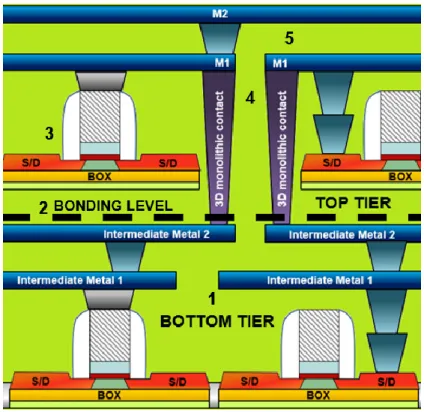
In a design perspective, the contact density among the tiers defines the maximum granularity, or in other words, in which design level the circuit can be partitioned between tiers. In Figure 1.2.3.4 the design granularity level is shown as four main flavors. The parallel integration is suitable for low-density contacts, enabling entire core or logic blocks 3D integration. On the other hand, the sequential process enables all the granularity scale, including logic gates (CMOS over CMOS) and transistor over transistor integrations.
Figure 1.2.3.4 Nanowire TEM image. The gate encloses all the channel; granting exceptional channel electrostatic control. [Batude 2014]
Figure 1.2.3.5 Comparison of 3D sequential process manufacturing strategies. [Batude 2011].
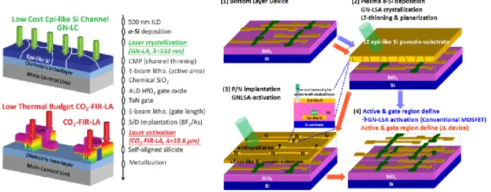
The monolithic process has several approaches in order to manufacture the top tier as categorized by [Batude 2011] seen in Figure 1.2.3.5. The main goal of the process is to achieve a good silicon lattice quality, and protect the already built tier by controlling the thermal budget. The seed window method creates a path for silicon seed from bottom wafer in order to recrystallize the top wafer. A second approach creates the transistor without the monocrystalline silicon in the top. The epitaxy-like silicon is done by a laser annealing; however the silicon layer is polycrystalline. Although the polycrystalline limits the transistor performance, the process is potentially low-cost. The process integration using laser annealing is shown in Figure 1.2.3.6 from [Shen 2013; T. T. Wu 2015].
Figure 1.2.3.6 Process flow for 3D sequential integration using Poly-Si laser recrystallization [Shen 2013; T. T. Wu 2015].
Finally, the process can be done by wafer bonding over an already processed tier. In this approach, the top wafer has already high-quality silicon. Thanks to its high alignment precision the process can reach ultra-fine pitch connection between tiers. As a result, ultra-high 3D contact densities (108 via/mm2 for a
14nm node stacking) is achieved [Batude 2011]. 2-tier integration with intermediate back-end (iBEOL) and 3D contacts (3DCO) is shown in Figure 1.2.3.7.
The challenge of such integration is to obtain a top level with similar bottom level performances; but with a limited thermal budget process. Depending on the considered technology and node, the maximal sustainable thermal budget by the bottom layer will differ. The bottom wafer is a standard process with routed metal layers (iBEOL). The bottom devices have to resist to the top highest process temperatures. For example, [Deprat 2016], [Fenouillet-Beranger 2014] show how a conventional 950°C annealing degrades the bottom tier performance. This restricts the thermal budget for the top tier, where all the front-end processes are limited to 500ºC during 2 hours for the 14nm FD-SOI technology, or more specifically a time-temperature window [Batude 2015]; hence in literature, this is referred as low temperature (LT). The bottom silicide is enhanced to become stable for this range of temperatures [Deprat 2016]. Tungsten is used as iBEOL metal due to the contamination risks in case of wafer breaking during the top processes in front-end machines. The LT monolithic process currently achieves the high performance in 14nm thanks to Solid Phase Epitaxy Regrowth (SPER)[Batude 2015] while keeping low variability [Pasini 2016]. The 3DCO are done sequentially after the top LT process using standard tungsten plug in oxide, connecting iBEOL to the final BEOL, which is a standard Cu/Low-k back-end. This process integration has been demonstrated on 300 mm wafers with one metal line of Tungsten in iBEOL [Brunet 2016] and its process flow is illustrated in Figure 1.2.3.8.
Figure 1.2.3.7 3D stack with sequential integration featuring homogenous process technologies, and intermediate back-end.
Figure 1.2.3.8 3D sequential design flow for CoolCubeTM process using wafer bonding and maximum temperature for critical steps [Brunet 2016].
The laser annealing can help the low temperature process as well, even for the wafer bonding integration. As the laser can concentrate high power in a small area, the heat is enough to do the dopant activation instead of SPER process, but the heat diffusion in a very short time is not sufficient to degrade the tier already built. This is an active topic in research for low temperature process as seen in Figure 1.2.3.9. For certain laser energy; the light can activate the junction. However, as the top tier is done over the already processed circuit, the bottom circuit may also contain back-end metals for interconnections routing, which is called intermediate back-end (iBEOL). The iBEOL metals can reflect some of the laser energy, influencing the heating process, as the power density per area is critical. Hence, the iBEOL metal pattern can change the outcome of the laser annealing [Fenouillet-Beranger 2016].
The 3D CoolCubeTM sequential integration is illustrated in Figure 1.2.3.10, in this case without iBEOL. The
3DCO vias between tiers shows excellent alignment precision.
Figure 1.2.3.9 Laser annealing for junction activation for low temperature 3D process. [Fenouillet-Beranger 2016].
Figure 1.2.3.10 3D sequential integration using bonded SOI wafer. The 3DCO processed after the bonding yields a high alignment precision [Brunet 2016].
The ultimate research goal is to produce low temperature stacked transistors with the same performance of standard planar process without degrading the bottom transistors, as illustrated in ION vs IOFF figures of
merit in Figure 1.2.3.11; showing the bottom MOSFET thermal stability and the possibility of high performance transistor using low temperature process.
Figure 1.2.3.11 Typical ION vs IOFF. On the left, (a) The bottom performance before the top process in black and after a thermal budget in red (Batude et al., 2014). On the right, low temperature process with different implant doses for the S/D compared to reference planar process in red [Pasini 2016].
The 3D process described uses the FDSOI as transistor architecture. Other processes have already been demonstrated to achieve 3D sequential integration featuring heterogeneous technologies [Shulaker 2014],[Irisawa 2014]. Indeed, the 3D monolithic process can feature different technologies in each tier in order to use the best potential of a given technology for a determined application, as illustrated in Figure 1.2.3.12. Such integration, can use FinFETs for high performance logic, and FDSOI on the top tier for
RF communications. This solution is infeasible and cost prohibitive in a planar monolithic integration, otherwise different processes have to be managed in the same masks.
Figure 1.2.3.12 Homogenous 3D integration featuring different transistor architectures in each tier [Batude 2014].
1.3 Thesis Objectives
As the Moore’s Scaling is approaching to materials physical limits, new solutions have been proposed: either continuing miniaturization and exploring new materials or doing more than scaling and adding more features to the circuit, such as integrating logic and sensors in the same monolithic circuit.
Evaluating a technology proposal among the crowd is the main goal of this thesis. Specifically, the 3D Sequential Integration (3DVLSI) is assessed in several design aspects, such as Performance/Power/Area (PPA) and Variability for digital circuits.
Most of the state of the art presented in Chapter One for 3D sequential circuits is based on advanced process. The automated design tools for 3DVLSI are under development. In this context, this thesis also provides guidelines for EDA development and process performance. The analyses are based on SPICE simulations.
In a succinct way, the work done consists in:
• 3D environment evaluation using SPICE and Full-Custom layouts • 3D Contacts operation assessment in final circuit performance • Area overhead and solutions for 3DVLSI
• Guidelines for EDA tools development and process performance guidance
• Assessment of variability – Global and Local variation impact in circuit figures of merit • Across-Chip Variations (ACV) modeling and its effects in 3D sequential circuits
The thesis has been divided into two distinct parts, the first one is focused on circuit design while the second part scrutinize the process variability impact on design.
1.4 Chapter Conclusion
The miniaturization of circuits has been presented as the main engine of the semiconductor industry research and development. The scaling trend that effectively took place over the last 50 years is discussed as the Moore’s Law and illustrated also as the roadmap of the industry.
The scaling reduced the transistor cost per node as suggest by Moore’s paper. Coupled to miniaturization, the better transistor performance due to reduce dimensions was noted by Dennard in 1975. Over the years, the circuits became cheaper and more powerful.
The traditional scaling, reducing dimensions and thicknesses finished in the 2000’s. Due to the current leakage and the need to increase device performance, new technical solutions were employed. Finally, in the 2010’s the transistor architecture was complete revamped to continue the trend. As the scaling is approaching to atomic scales and becoming more difficult, new solutions like 3D integration were proposed. Stacking tiers can bring benefits to circuits considering the PPA and augment the function capabilities (such logic integration with sensors).
Semiconductor 3D integration can be classified as parallel and sequential integration. Both state of the art for the process has been illustrated in Chapter One. The parallel integration has the advantage to use a standard planar process like, having the wafers bonded after, with minor modifications to create the through silicon vias (TSV) to contact tiers. Due to the bonding step, the misalignment between wafers is a limiting factor and this issue is mitigated by a large TSV size in order to grant the contact. This creates a huge area overhead, limiting the connection density between the tiers. The problem can be completely avoided by stacking the tiers aligned, in a 3D sequential process. This enables an ultra-high 3D contact density among the tiers. The main disadvantage of such an approach is the top processes with a limited thermal budget, in order not to damage the already processed tier. The state of the art of low temperature process for 3D integration has been discussed in Chapter One. With ultra-high density 3DCO and high transistor performance for both tiers, the sequential 3DVSLI is shown as a perfect candidate for digital logic circuits to continue the scaling in a more than Moore’s flavor.
REFERENCES
Barraud, S., R. Coquand, M. Casse, M. Koyama, J. M. Hartmann, V. Maffini-Alvaro, C.
Comboroure, et al. 2012. “Performance of Omega-Shaped-Gate Silicon Nanowire
MOSFET With Diameter Down to 8 Nm.” IEEE Electron Device Letters 33 (11): 1526–
28. doi:10.1109/LED.2012.2212691.
Batude, P., C. Fenouillet-Beranger, L. Pasini, V. Lu, F. Deprat, L. Brunet, B. Sklenard, et al. 2015.
“3DVLSI with CoolCube Process: An Alternative Path to Scaling.” In 2015 Symposium on
VLSI Technology (VLSI Technology), T48–49. doi:10.1109/VLSIT.2015.7223698.
Batude, P., B. Sklenard, C. Fenouillet-Beranger, B. Previtali, C. Tabone, O. Rozeau, O. Billoint, et
al. 2014. “3D Sequential Integration Opportunities and Technology Optimization.” In IEEE
International
Interconnect
Technology
Conference,
373–76.
doi:10.1109/IITC.2014.6831837.
Batude, P., M. Vinet, B. Previtali, C. Tabone, C. Xu, J. Mazurier, O. Weber, et al. 2011. “Advances,
Challenges and Opportunities in 3D CMOS Sequential Integration.” In 2011 International
Electron Devices Meeting, 7.3.1-7.3.4. doi:10.1109/IEDM.2011.6131506.
Batude, P., M. Vinet, C. Xu, B. Previtali, C. Tabone, C. Le Royer, L. Sanchez, et al. 2011.
“Demonstration of Low Temperature 3D Sequential FDSOI Integration down to 50 Nm
Gate Length.” In 2011 Symposium on VLSI Technology - Digest of Technical Papers, 158–
59.
Brunet, L., P. Batude, C. Fenouillet-Beranger, P. Besombes, L. Hortemel, F. Ponthenier, B.
Previtali, et al. 2016. “First Demonstration of a CMOS over CMOS 3D VLSI CoolCube
#x2122; Integration on 300mm Wafers.” In 2016 IEEE Symposium on VLSI Technology,
1–2. doi:10.1109/VLSIT.2016.7573428.
Chen, J., T. Y. Chan, I. C. Chen, P. K. Ko, and C. Hu. 1987. “Subbreakdown Drain Leakage Current
in
MOSFET.”
IEEE
Electron
Device
Letters
8
(11):
515–17.
doi:10.1109/EDL.1987.26713.
Chen, K. N., and C. S. Tan. 2011. “Integration Schemes and Enabling Technologies for
Three-Dimensional Integrated Circuits.” IET Computers Digital Techniques 5 (3): 160–68.
doi:10.1049/iet-cdt.2009.0127.
Cristoloveanu, S. 1999. “SOI: A Metamorphosis of Silicon.” IEEE Circuits and Devices Magazine
15 (1): 26–32. doi:10.1109/101.747564.
Dennard, R. H., F. H. Gaensslen, V. L. Rideout, E. Bassous, and A. R. LeBlanc. 1974. “Design of
Ion-Implanted MOSFET’s with Very Small Physical Dimensions.” IEEE Journal of
Solid-State Circuits 9 (5): 256–68. doi:10.1109/JSSC.1974.1050511.
Dennard, R. H., F. H. Gaensslen, Hwa-Nien Yu, V. L. Rideout, E. Bassous, and A. R. Leblanc.
1999. “Design Of Ion-Implanted MOSFET’s with Very Small Physical Dimensions.”
Proceedings of the IEEE 87 (4): 668–78. doi:10.1109/JPROC.1999.752522.
Deprat, F., F. Nemouchi, C. Fenouillet-Beranger, M. Cassé, P. Rodriguez, B. Previtali, N. Rambal,
et al. 2016. “First Integration of Ni0.9Co0.1 on pMOS Transistors.” In 2016 IEEE
International Interconnect Technology Conference / Advanced Metallization Conference
(IITC/AMC), 133–35. doi:10.1109/IITC-AMC.2016.7507708.
Ernst, T., L. Duraffourg, C. Dupre, E. Bernard, P. Andreucci, S. Becu, E. Ollier, et al. 2008. “Novel
Si-Based Nanowire Devices: Will They Serve Ultimate MOSFETs Scaling or Ultimate
Hybrid Integration?” In 2008 IEEE International Electron Devices Meeting, 1–4.
doi:10.1109/IEDM.2008.4796804.
Fenouillet-Beranger, C., P. Acosta-Alba, B. Mathieu, S. Kerdilès, M. P. Samson, B. Previtali, N.
Rambal, et al. 2016. “Ns Laser Annealing for Junction Activation Preserving Inter-Tier
Interconnections Stability within a 3D Sequential Integration.” In 2016 IEEE
SOI-3D-Subthreshold Microelectronics Technology Unified Conference (S3S), 1–2.
doi:10.1109/S3S.2016.7804375.
Fenouillet-Beranger, C., B. Previtali, P. Batude, F. Nemouchi, M. Cassé, X. Garros, L. Tosti, et al.
2014. “FDSOI Bottom MOSFETs Stability versus Top Transistor Thermal Budget
Featuring 3D Monolithic Integration.” In 2014 44th European Solid State Device Research
Conference (ESSDERC), 110–13. doi:10.1109/ESSDERC.2014.6948770.
Fujii, H., K. Miyaji, K. Johguchi, K. Higuchi, C. Sun, and K. Takeuchi. 2012. “x11 Performance
Increase, x6.9 Endurance Enhancement, 93% Energy Reduction of 3D TSV-Integrated
Hybrid ReRAM/MLC NAND SSDs by Data Fragmentation Suppression.” In 2012
Symposium on VLSI Circuits (VLSIC), 134–35. doi:10.1109/VLSIC.2012.6243826.
Gargini, P. A. 2017. “How to Successfully Overcome Inflection Points, or Long Live Moore’s
Law.” Computing in Science Engineering 19 (2): 51–62. doi:10.1109/MCSE.2017.32.
Hsieh, A. C., and T. Hwang. 2012. “TSV Redundancy: Architecture and Design Issues in 3-D IC.”
IEEE Transactions on Very Large Scale Integration (VLSI) Systems 20 (4): 711–22.
doi:10.1109/TVLSI.2011.2107924.
Huang, Hsiang-Jen, Kun-Ming Chen, Tiao-Yuan Huang, Tien-Sheng Chao, Guo-Wei Huang,
Chao-Hsin Chien, and Chun-Yen Chang. 2001. “Improved Low Temperature
Characteristics of P-Channel MOSFETs with Si1-xGex Raised Source and Drain.” IEEE
Transactions on Electron Devices 48 (8): 1627–32. doi:10.1109/16.936576.
Huang, P. T., S. L. Wu, Y. C. Huang, L. C. Chou, T. C. Huang, T. H. Wang, Y. R. Lin, et al. 2014.
“2.5D Heterogeneously Integrated Microsystem for High-Density Neural Sensing
Applications.” IEEE Transactions on Biomedical Circuits and Systems 8 (6): 810–23.
doi:10.1109/TBCAS.2014.2385061.
Huynh-Bao, T., J. Ryckaert, Z. Tökei, A. Mercha, D. Verkest, A. V. Y. Thean, and P. Wambacq.
2017. “Statistical Timing Analysis Considering Device and Interconnect Variability for
BEOL Requirements in the 5-Nm Node and Beyond.” IEEE Transactions on Very Large
Scale Integration (VLSI) Systems PP (99): 1–12. doi:10.1109/TVLSI.2017.2647853.
Irisawa, T., K. Ikeda, Y. Moriyama, M. Oda, E. Mieda, T. Maeda, and T. Tezuka. 2014.
“Demonstration of Ultimate CMOS Based on 3D Stacked InGaAs-OI/SGOI Wire Channel
MOSFETs with Independent Back Gate.” In 2014 Symposium on VLSI Technology
(VLSI-Technology): Digest of Technical Papers, 1–2. doi:10.1109/VLSIT.2014.6894395.
Knickerbocker, J. U., P. S. Andry, E. Colgan, B. Dang, T. Dickson, X. Gu, C. Haymes, et al. 2012.
“2.5D and 3D Technology Challenges and Test Vehicle Demonstrations.” In 2012 IEEE
62nd
Electronic
Components
and
Technology
Conference,
1068–76.
doi:10.1109/ECTC.2012.6248968.
Lee, D. U., K. W. Kim, K. W. Kim, H. Kim, J. Y. Kim, Y. J. Park, J. H. Kim, et al. 2014. “25.2 A
1.2V 8Gb 8-Channel 128GB/S High-Bandwidth Memory (HBM) Stacked DRAM with
Effective Microbump I/O Test Methods Using 29nm Process and TSV.” In 2014 IEEE
International Solid-State Circuits Conference Digest of Technical Papers (ISSCC), 432–
33. doi:10.1109/ISSCC.2014.6757501.
Lin, Y. H., S. Y. Huang, K. H. Tsai, W. T. Cheng, S. Sunter, Y. F. Chou, and D. M. Kwai. 2013.
“Parametric Delay Test of Post-Bond Through-Silicon Vias in 3-D ICs via Variable Output
Liu, C., and S. K. Lim. 2012. “A Design Tradeoff Study with Monolithic 3D Integration.” In
Thirteenth International Symposium on Quality Electronic Design (ISQED), 529–36.
doi:10.1109/ISQED.2012.6187545.
Mistry, K., C. Allen, C. Auth, B. Beattie, D. Bergstrom, M. Bost, M. Brazier, et al. 2007. “A 45nm
Logic Technology with High-k+Metal Gate Transistors, Strained Silicon, 9 Cu Interconnect
Layers, 193nm Dry Patterning, and 100% Pb-Free Packaging.” In 2007 IEEE International
Electron Devices Meeting, 247–50. doi:10.1109/IEDM.2007.4418914.
Moore, G. E. 1998. “Cramming More Components Onto Integrated Circuits.” Proceedings of the
IEEE 86 (1): 82–85. doi:10.1109/JPROC.1998.658762.
Pasini, L., P. Batude, J. Lacord, M. Casse, B. Mathieu, B. Sklenard, F. P. Luce, et al. 2016. “High
Performance CMOS FDSOI Devices Activated at Low Temperature.” In 2016 IEEE
Symposium on VLSI Technology, 1–2. doi:10.1109/VLSIT.2016.7573407.
Plas, G. Van der, P. Limaye, I. Loi, A. Mercha, H. Oprins, C. Torregiani, S. Thijs, et al. 2011.
“Design Issues and Considerations for Low-Cost 3-D TSV IC Technology.” IEEE Journal
of Solid-State Circuits 46 (1): 293–307. doi:10.1109/JSSC.2010.2074070.
Rozeau, O., J. Lacord, S. Martinie, Anouar Idrissi-El Oudrhiri, M. A. Jaud, S. Barraud, T. Poiroux,
M. Vinet, and J. C. Barbé. 2015. “Performance Benchmarking of Device Architectures for
the Sub-10nm CMOS Technologies.” In The 5th International Workshop on
Nanotechnology and Application (IWNA)).
Schwarzenbach, W., X. Cauchy, F. Boedt, O. Bonnin, E. Butaud, C. Girard, B. Y. Nguyen, C.
Mazure, and C. Maleville. 2011. “Excellent Silicon Thickness Uniformity on Ultra-Thin
SOI for Controlling Vt Variation of FDSOI.” In 2011 IEEE International Conference on
IC Design Technology, 1–3. doi:10.1109/ICICDT.2011.5783188.
Shen, C. H., J. M. Shieh, T. T. Wu, W. H. Huang, C. C. Yang, C. J. Wan, C. D. Lin, et al. 2013.
“Monolithic 3D Chip Integrated with 500ns NVM, 3ps Logic Circuits and SRAM.” In 2013
IEEE
International
Electron
Devices
Meeting,
9.3.1-9.3.4.
doi:10.1109/IEDM.2013.6724593.
Shulaker, M. M., T. F. Wu, A. Pal, L. Zhao, Y. Nishi, K. Saraswat, H. S. P. Wong, and S. Mitra.
2014. “Monolithic 3D Integration of Logic and Memory: Carbon Nanotube FETs, Resistive
RAM, and Silicon FETs.” In 2014 IEEE International Electron Devices Meeting,
27.4.1-27.4.4. doi:10.1109/IEDM.2014.7047120.
Thompson, S. E., M. Armstrong, C. Auth, M. Alavi, M. Buehler, R. Chau, S. Cea, et al. 2004. “A
90-Nm Logic Technology Featuring Strained-Silicon.” IEEE Transactions on Electron
Devices 51 (11): 1790–97. doi:10.1109/TED.2004.836648.
Weber, O., F. Andrieu, J. Mazurier, M. Cassé, X. Garros, C. Leroux, F. Martin, et al. 2010.
“Work-Function Engineering in Gate First Technology for Multi-VT Dual-Gate FDSOI CMOS on
UTBOX.” In 2010 International Electron Devices Meeting, 3.4.1-3.4.4.
doi:10.1109/IEDM.2010.5703289.
Wu, S. Y., C. Y. Lin, M. C. Chiang, J. J. Liaw, J. Y. Cheng, C. H. Chang, V. S. Chang, et al. 2016.
“Demonstration of a Sub-0.03 um2 High Density 6-T SRAM with Scaled Bulk FinFETs
for Mobile SOC Applications beyond 10nm Node.” In 2016 IEEE Symposium on VLSI
Technology, 1–2. doi:10.1109/VLSIT.2016.7573390.
Wu, T. T., C. H. Shen, J. M. Shieh, W. H. Huang, H. H. Wang, F. K. Hsueh, H. C. Chen, et al.
2015. “Low-Cost and TSV-Free Monolithic 3D-IC with Heterogeneous Integration of
Logic, Memory and Sensor Analogy Circuitry for Internet of Things.” In 2015 IEEE
INTRODUCTION TO CHAPTER TWO
3D sequential integration, or 3DVLSI is the proposed alternative to the Moore’s Law scaling. The stacking of transistors in several tiers can increase the circuit density for a given area, and optimizations in back-end interconnections can improve the circuit performance and reduce the power usage. This chapter explores the 3D design environment focusing ultra-dense logic circuits, and benchmark several aspects of the 3D monolithic circuits.
At the present time (2017); logic circuits such as Graphic Processor Units (GPUs) have more than 15 billion transistors. In order to achieve an architecture with so many elements, a well-established design methodology is used in planar circuits. In this chapter, those techniques are synthetized in a brief introduction. The 3DVLSI design tools are under development; but are mainly based in planar as an inheritance. The work has been done using a 3D Process Design Kit (PDK), constantly having upgrades as the technology is under evolution. The technology hypotheses and their implications in the design are discussed completing the chapter introduction.
Design-wisely, the high density of 3D Contacts (3DCO) through the tiers allows several integration implementations. Solutions such as CMOS over CMOS and Transistor over Transistors are discussed and compared. This work is largely based on the design of full custom circuits, as placement and routing design tools are not commercially available.
2.1 VLSI Digital Design Flow
2.1.1 Overview in Planar Design Flow
The automated design flow in Very-Large Scale Integration (VLSI) is composed by various stages. As a natural evolution during the years, the abstraction level has increased in order to manage complex circuits having billions of transistors.
Figure 2.1.1.1 Usual digital design flow methodology in advanced planar nodes.
The big picture of the digital design flow, divided into five macroscopic steps, is shown in Figure 2.1.1.1. The circuit design is done by coding at high abstraction level, such as Register-Transfer Level (RTL) using VHDL or Verilog languages. The combinational and sequential logic are described by the code and later are


![Figure 1.2.3.8 3D sequential design flow for CoolCube TM process using wafer bonding and maximum temperature for critical steps [Brunet 2016]](https://thumb-eu.123doks.com/thumbv2/123doknet/12863055.368701/38.918.118.810.143.426/figure-sequential-coolcube-process-bonding-maximum-temperature-critical.webp)
![Figure 1.2.3.10 3D sequential integration using bonded SOI wafer. The 3DCO processed after the bonding yields a high alignment precision [Brunet 2016]](https://thumb-eu.123doks.com/thumbv2/123doknet/12863055.368701/39.918.118.811.108.421/figure-sequential-integration-processed-bonding-alignment-precision-brunet.webp)


