HAL Id: hal-01197043
https://hal.archives-ouvertes.fr/hal-01197043
Submitted on 11 Sep 2015
HAL is a multi-disciplinary open access
archive for the deposit and dissemination of
sci-entific research documents, whether they are
pub-lished or not. The documents may come from
teaching and research institutions in France or
abroad, or from public or private research centers.
L’archive ouverte pluridisciplinaire HAL, est
destinée au dépôt et à la diffusion de documents
scientifiques de niveau recherche, publiés ou non,
émanant des établissements d’enseignement et de
recherche français ou étrangers, des laboratoires
publics ou privés.
Highly integrated power electronic converters using
active devices embedded in printed-circuit board
Chenjiang Yu, Cyril Buttay, Eric Labouré, Vincent Bley, Céline Combettes
To cite this version:
Chenjiang Yu, Cyril Buttay, Eric Labouré, Vincent Bley, Céline Combettes.
Highly integrated
power electronic converters using active devices embedded in printed-circuit board. 4th
Micro/Nano-Electronics, packaging and assembling, design and manufacturing forum MiNaPAD 2015, IMAPS,
Apr 2015, Grenoble, France. �hal-01197043�
Highly integrated power electronic converters using active
devices embedded in printed-circuit board
Chenjiang Y
U1, Cyril B
UTTAY2, ´Eric L
ABOURE´
1, Vincent B
LEY3, C´eline C
OMBETTES31LGEP (GEEPS)
CentraleSupelec Univ. Paris-Sud, UPMC, CNRS
11 rue Joliot Curie Plateau de Moulon, F91192, France
2Universit´e de Lyon
CNRS, UMR5005 INSA-Lyon Laboratoire Amp`ere,
bˆatiment L. de Vinci, 21 avenue Capelle F-69621, France
3Universit´e de Toulouse; UPS, INPT;
LAPLACE;
118 route de Narbonne - Bˆat. 3R3 F-31062 Toulouse cedex 9, France.
CNRS; LAPLACE; F-31062 Toulouse, France
Abstract
In this paper, we present a short overview of the power dies interconnects based on PCB technology, then we focus on embedding of power dies in the PCB material. In the second part of the article, we present in details the technology we developed to embed dies in PCB. Results show that the electrical performance of the die remains satisfying after embedding, but that dies with a copper topside metal layer are required for this process.
Keywords
3-D packaging, PCB, DBC
1
Introduction
Current and future power semiconductor devices (espe-cially those based on silicon carbide – SiC – or gallium nitride – GaN –) offer very high switching speed capabil-ity. Current fast transistor can switch currents of several kiloamperes per microsecond, and voltages of more than 10 kilovolts per microsecond. This makes it possible to increase the conversion efficiency (shorter switching tran-sient, hence lower switching losses), or to reduce the size of the converters (by increasing their switching frequency and using smaller passive components). To take full ad-vantage of these fast devices, it is, however, necessary to design very-low inductance interconnects. For example, in [1], the authors present a switching cell with a sub-nanohenry stray inductance designed for GaN transistors. They also integrate the gate-drive circuit to supply fast control signals to the transistors. For such high-density interconnects, the printed-circuit board (PCB) technology is very attractive. Another clear trend in power electron-ics is the increase in power density. As a consequence, and despite the improvement in conversion efficiency, the active devices dissipate a lot of heat (100 to 300 W/cm²). Therefore, they must be attached to a low-thermal resis-tance cooling system. Classically, ceramic substrates (es-pecially DBC, for Direct Bonded Copper) are used [2]. In this paper, we focus on packaging solutions where active
dies are attached on a DBC substrate (for thermal man-agement), and then embedded in layers of PCB. We start by presenting a review of the existing solutions from the literature, and then we present some prototypes we assem-bled in the lab.
2
Review of PCB-based Die
inter-connects and of Die Embedding in
PCB
Although it can be found virtually everywhere, the “stan-dard” power electronics interconnection technique (wire-bonding) has many drawbacks: as discussed above, it gen-erates relatively large stray inductances (several nanohen-ries); it occupies a non-negligible area on the substrate (all the interconnections are performed on the same plane); it is time-consuming to manufacture (all wirebonds must be placed successively).
As a consequence, many researcher have tried to over-come these limitations. Among the various solutions pro-posed, we will focus on those that make use of flexible or rigid PCB technology. Indeed, this technology is very mature, offers a variety of interconnect possibilities, and makes it possible to process many dies at once.
based on the flex PCBs: once they are populated with the components (in standard Surface-Mount Technology, SMT), they can be rolled around the larger component [3] or folded in a sophisticated fashion [4]. Such approach may make thermal management difficult, and seems more suited to low-power converters (up to a few hundred watts).
Another use of the flex PCB is as direct replacement for the wirebonds: the power semiconductor dies are at-tached to a DBC substrate, and a flex PCB is atat-tached on top of the devices. This flex PCB also provides the inter-connections between the topside of the dies and the DBC substrate if needed. Such solution requires dies with a suitable topside metal [5] (most power dies have an alu-minium layer, which is suited to wirebonding, but not to soldering or sintering). Compared to wirebonds, the flex PCB offers higher interconnect density [6], especially be-cause it can have several layers. Furthermore, auxiliary components (such as the gate drivers) can be mounted di-rectly on the flex PCB [7]. Commercial power modules that use flex PCB instead of wirebonds are available from Semikron [8].
Another set of solutions is based on rigid PCBs rather than flex. Rigid PCBs are thicker (from a few hundred of microns up to a few millimeters), so it is possible to integrate devices inside the PCB. For example, various manufacturers sell dielectric layers that can be stacked in a multilayer PCB to form capacitors [9]. An example of a converter integrating such capacitive layers is given in [10]. In this paper, the authors also embed some mag-netic layers to form an “embedded Passive Integrated Cir-cuit” (emPIC).
However, most papers focus on integrating the active rather than the passive devices in the PCB. This allows for a shorter distance between the active die and the cool-ing system. PCBs have poor thermal conductivity (usually lower than 1 W/m.K, as compared to 24 W/m.K for alu-mina or 150 W/m.K for AlN ceramics), and power semi-conductor devices have a high power density to dissipate (100 W/cm2or more).
Some authors do not use the PCB material, but the structure they propose offer many features of PCB-embedding. For example, in [11], power dies are attached on a DBC and integrated in a ceramic frame. In [12], a polyimide (Kapton) layer is used around the dies. Fi-nally, the “SiPLIT” technology [13], uses some steps of the PCB technology (lamination, electroplating) to form a power module with very low parasitic inductances.
A list of commercially-available, PCB integration tech-nologies for active devices (not limited to power devices) is given in [14]. Many of these technologies were de-veloped through the European projects “Hermes” and “Hiding Dies”, or through the German project “HiLevel”. These projects included work on the manufacturing
tech-nology, on the design tools, and on validation [15]. In particular, one of the demonstrators of the “HiLevel” project included a 50 kW inverter for hybrid cars. It is described in [16]: the dies are attached to a thick copper layer (no DBC used here), and then embedded in PCB laminates. The pads of the dies are then exposed by re-moving some of the PCB material with a laser.
In [17], the exposition of the pads is performed by me-chanically grinding away some of the PCB materials. The resulting converter offers very low parasitic inductances, and allows for very close decoupling, as the decoupling capacitors are mounted directly on top of the power semi-conductor dies.
Other technologies use a “face down” approach, where the dies are first attached in a “flip-chip” orientation to a patterned copper foil. This seems more suited to high-density chips such as microprocessors [18].
3
Proposed Embedding Technique
3.1
Overview of the process
The process flow of the proposed embedding technique is visible in figure 1.
The dies are first attached to a patterned DBC substrate using silver sintering (fig 1a). This technology offers high electrical and thermal performance, and can sustain the remaining manufacturing steps. As it is a solid-state pro-cess, there is no movement of the dies during sintering (as opposed to soldering, where dies usually move slightly during reflow). This is very important, as a good position-ing accuracy (in the order of 100 µm for power devices) is required later to contact the topside of the dies.
Then, we stack a set of pre-impregnated sheets of glass fibre (with the shape of the dies cut-out) on top of the DBC/die assembly, plus a sheet of copper (fig. 1b). This stack is then laminated under pressure, using the stan-dard PCB manufacturing technology (fig. 1c). The copper layer is open above the dies (using standard PCB lithog-raphy and wet-etching) (fig. 1d). A CO2laser is used to
ablate the glass fiber/resin composite exposed through the windows in the copper layer (fig. 1e). It is worth not-ing that although it is relatively thin (3 µm) the topside metal of the devices is not damaged by the laser. Fi-nally, an electroplating process (identical to the process used for PCB through-hole plating) allows to connect the topside pads of the embedded dies with the top copper layer (fig. 1f. From this step, the resulting assembly can be used as a standard PCB, allowing to pattern the copper layer, to add more layers (for higher circuit complexity), and to attach surface-mount components (passives, gate drivers, etc.)
In the following sections, we give some more practical details on this process
(a) (b) (c) (d) (e) (f)
Figure 1: Die embedding technique proposed in this paper: (a) a die is attached to a DBC substrate. Layers of laser-cut prepreg foils are then stacked around the die (b) with a copper foil on top, and laminated (c). Windows are etched in the copper layer (d), and used as a mask for the laser-ablation of the PCB material (e). Finally, copper is electroplated on the top surface (f).
3.2
Preparation and mounting of the dies
The dies used in this paper are 1200 V, silicon diodes with a die size of 9×9 mm2. They have a standard backsidesilver finish, and a topside aluminium metallization (quired for aluminium wirebonds). Some of the diodes re-ceived layers of Ti/Cu (deposited by PVD through a poly-imide mask, with thicknesses of 50/150 nm, in an EVA300 system) on their topside.
The diodes were then mounted on bare copper sub-strates using the following pressure-less silver-sintering process:
• screen printing of Heraeus LTS 117O2P2 silver paste (thickness 50 µm). The printed pattern consists in 16 smaller squares with a 300 µm spacing between them to form the 9×9 mm2footprint. This is used
to achieve better drying of the paste despite the large surface area of the dies;
• placement of the die on top of the fresh paste de-posit using a JPF Microtechnic PPOne die bonder (for proper alignment and control of the force applied on the die, around 0.1 N);
• drying of the paste, 85 °C for 30 min;
• sintering stage: fast ramp-up (70 °C/min) up to 240 °C, and 30 min maintained at 240 °C.
• natural cooling down
The process takes place in air, causing the bare copper substrates to oxidize, but this was not an issue for the fol-lowing steps.
3.3
PCB embedding
Two reference of prepreg sheets are used for the PCB em-bedding: Isola PCL 370HR (high Tg FR4 material) and Arlon 55NT (non-woven epoxy-aramide material).
The FR4 material is used in the stacking to match the die thickness, and a cutout slightly larger than the diode is performed in the sheets of prepreg (fig. 1b). 3 layers of prepreg are stacked.
The non-woven material is used as the topmost layer, the one that covers the diode (fig. 1b). It is used because the laser ablation which comes later in the process leaves fewer residues on the surface of the die. It is, however, a more expensive material than FR4, which is why it was not used for the whole prepreg stack. Finally, a sheet of copper (35 µm) is added to the stack prior to lamination, which is performed under 13 bars and 195 °C for 90 min-utes in an LPKF Multipress S laminator.
After lamination, the topside copper layer is etched away to open a window corresponding to the pads of the
embedded die (fig. 1d). This step requires proper align-ment with the die, but this remain less demanding than any High-Density Interconnect (HDI) multi-layer PCB, a technology which is commonplace nowadays [18]. A po-sitioning accuracy of 100 µm is sufficient to match the smallest pad size of a power die (typically the gate con-tact on a MOSFET or an IGBT, which is designed to be connected with a 100-125 µm wedge wirebond.
Laser ablation of the laminate material is performed on a Gravograph LS100EX 60 watt CO2laser (10.6 µm
wavelength). Preliminary tests showed that the parame-ters of the laser (namely sweep speed and power of the beam) had little influence on the quality of the result, pro-viding the beam is slow enough or powerful enough to remove the organic material. In all cases, we did not ob-serve any change in the appearance of the topside metal of the dies. This is very interesting, as it demonstrates a very good selectivity of the laser ablation: it easily re-moves the laminate, but stops completely once it reaches the die. Another advantage of this good selectivity is that we can use the laminated copper layer as a mask for the laser ablation process: there is no need for accurate align-ment of the laser with the chips; a coarse positioning is sufficient, providing the laser sweeps an area larger than the openings in the copper layer.
As the ablation is performed in air, cleaning in iso-propanol is required to remove some residues. A protec-tive atmosphere (N2) should help reducing these residues.
The last step of the embedding process is the electro-plating of a copper layer over the entire surface of the PCB, including the die cutouts (fig. 1f). We use the stan-dard “plated-through-hole” process (Bungard).
Once this process is over, the resulting DBC/PCB can be handled like a standard PCB: etching of a pattern in the topside copper, lamination of more layers, reflow solder-ing of SMT components, etc. The only restriction applies to the drilling of vias: only blind vias are allowed, as the ceramic material of the DBC is too hard for the drill bits.
4
Results
4.1
process parameters
Two sets of dies were processed as described in fig. 1: the first set was used as supplied, while the second set received a PVD plating (Ti/Cu) over its aluminium topside metallization.
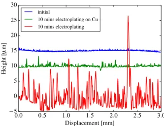
The surface roughness of the metal on top of the dies was measured using a stylus profilometer (Tencor), and some of the results are presented in figure 2. The blue line (top) corresponds to a measurement performed on the Al metallization before any treatment. The green line (mid-dle) is the surface profile of an embedded die which re-ceived a Ti/Cu plating and the red plot (bottom) is the
0.0 0.5 1.0 1.5 2.0 2.5 3.0 Displacement [mm] −5 0 5 10 15 20 25 30 Height [µ m] initial 10 mins electroplating on Cu 10 mins electroplating
Figure 2: Surface roughness (stylus profilometer measurement) of a die before processing (initial), and after processing. The die that received a PVD plating of Ti/Cu before embedding shows a much lower roughness than the die that was directly embedded (with standard Al topside metal). The plots are shifted vertically for better clarity.
surface profile of an embedded die without Ti/Cu plating (the electroplating process was performed directly on the Al topside metal of the diode).
While both the green and red plots show an increase in roughness compared to the initial measurement (blue), this increase is moderate in the case of the die that re-ceived a Ti/Cu plating prior to the electroplating process. This is especially true when considering the thickness of the copper layer (3–10 µm) which is electroplated. In the case of the direct electroplating on aluminium, however, the surface roughness is much worse, with a peak of up to 25 µm. This confirms the visual aspect of the dies after electroplating: in the case of the Al dies, the electroplated copper is dull, while it is shiny in the case of the dies which received a Ti/Cu plating.
As a consequence, and despite it requires an extra pro-cessing step, a Ti/Cu plating of the dies seems neces-sary to improve the quality of the topside contact in our embedding process. This is in agreement with some of the processes described in the introduction, which require copper-finished dies. These are becoming more com-mon nowadays, because of the development of copper wirebonds [19], but they remain a minority compared to aluminium-finished dies.
4.2
Electrical characterization
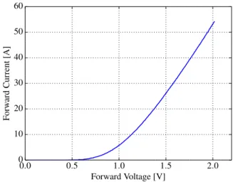
The static characterization of an embedded diode is pre-sented in figures 5 and 6. The forward characteristic was measured using a Tektronix 371A high power curve tracer, with 4-points connections to the PCB substrate. The series resistance of this diode (slope of the linear part
Copper substrate
Alignment pins
Exposed pad of the
embedded die
Cathode contact
Anode
contact
Figure 3: Sample used for electrical characterization (60×60 mm2). A diode with an aluminium topside metal was
used, which explains the dull aspect of the electroplated copper on the exposed pad.
Silicon die
Silver
Copper
Prepreg
Figure 4: Cross-section of the sample pictured in figure 3, taken at the edge of the exposed pad. The poor quality of the copper electroplated on the die is clearly visible.
of fig. 5) is high. This is due to the poor quality and low thickness of the electroplated copper layer (see fig. 4).
The reverse characteristic (figure 6) was measured us-ing a Keithley 2410 high-voltage SMU up to 1100V (lim-ited by the equipment. A second measurement was per-formed using the Tektronix 371A in high voltage mode. This second measurement is much less accurate, but in-dicates that the breakdown voltage of this embedded die occurs at around 1350 V. This shows that no arcing was detected, and that the embedding of the die constitutes a satisfying encapsulation. Further work is required to as-sess this encapsulation, especially in presence of moisture or after thermal cycling.
5
Conclusion and Perspectives
Embedding of dies in PCB material is a promising tech-nology, It allows for more compact systems, makes it
pos-0.0 0.5 1.0 1.5 2.0 Forward Voltage [V] 0 10 20 30 40 50 60 Forw ard Current [A]
Figure 5: Forward characteristic of the embedded die
−1200 −1000 −800 −600 −400 −200 0 Reverse voltage [V] 10−8 10−7 10−6 10−5 Re verse current [A]
Figure 6: Reverse characteristic of the embedded die
sible to process many dies at once, and offers superior electrical performance compared to wirebonding. The thermal performance of PCB, however, is often not suf-ficient for power electronics applications above a few tens or hundreds of watts.
Therefore, a solution is to use a substrate such as DBC for the thermal management, and to laminate PCB layers on top, for the electrical interconnects. This was already presented in the literature, by several research groups (section 2). However, most of the results that can be found (from companies and organizations such as AT&S, Schweizer, Fraunhofer IZM) rely on advanced equipment designed for large scale manufacturing of PCBs. Such equipment can only be afforded by a few research groups. Here, we presented in details the embedding process we developed, based on prototyping-scale PCB equipment. Although not as accurate as the state of the art machines for PCB manufacturing, this allows for low cost evalua-tion of the embedding technology.
A simple demonstrator is presented in the paper (a diode attached on a copper substrate using silver sinter-ing, and embedded in PCB). Electrical characterizations show satisfying forward and reverse characteristic of the packaged die.
The current work is focused on embedding several dies at once (diodes and transistors), to form a complete switching cell (including DC capacitors). This is neces-sary for the characterization of the dynamic behaviour of the packaging.
6
Acknowledgement
The authors thank the French National Agency for Re-search (ANR) for their financial support of this work, through the grant “ETHAER”; the 3DPHI national plat-form for giving access to their equipment; and Mr Gilles
BRILLAT(Univ. Paul SABATIER, Toulouse) for his
tech-nical assistance.
References
[1] K. Klein, E. Hoene, and K.-D. Lang, “Packages for Fast Switching HV GaN Power Devices.” in Proceedings of the PCIM 2014 conference, 2014.
[2] W. W. Sheng and R. P. Colino, Power Electronic Modules: Design and Manufacture, 1st ed. CRC, jun 2004. [3] A. B. Lostetter, F. Barlow, A. Elshabini, O. K., and S. Ang,
“Polymer Thick-Film (PTF) and Flex Technologies for Low Cost Power Electronics Packaging,” in Proceedings of the International Workshop on Integrated Power Pack-aging (IWIPP), 2000, pp. 33 – 40.
[4] E. de Jong, E. de Jong, B. Ferreira, and P. Bauer, “Toward the Next Level of PCB Usage in Power Electronic Con-verters,” Power Electronics, IEEE Transactions on, vol. 23, no. 6, pp. 3151–3163, 2008.
[5] X. Liu, S. Haque, and G.-Q. Lu, “Three-dimensional flip-chip on flex packaging for power electronics applications,” Advanced Packaging, IEEE Transactions on, vol. 24, no. 1, pp. 1–9, Feb 2001.
[6] S. Dieckerhoff, T. Kirfe, T. Wernicke, C. Kallmayer, A. Ostmann, E. Jung, B. Wunderle, and H. Reichl, “Elec-tric Characteristics of Planar Interconnect Technologies for Power MOSFETs,” in Power Electronics Specialists Con-ference, 2007. PESC 2007. IEEE, jun 2007, pp. 1036 – 1042.
[7] Y. Xiao, H. Shah, R. Natarajan, E. J. Rymaszewski, T. Chow, and R. Gutmann, “Integrated flip-chip flex-circuit packaging for power electronics applications,” Power Electronics, IEEE Transactions on, vol. 19, no. 2, pp. 515– 522, March 2004.
[8] T. Stockmeier, P. Beckedahl, C. Gobl, and T. Malzer, “SKiN: Double side sintering technology for new pack-ages,” in Power Semiconductor Devices and ICs (ISPSD),
2011 IEEE 23rd International Symposium on, May 2011, pp. 324–327.
[9] J. Andresakis, “Embedded Capacitors,” Oak-Mitsui Technologies, presentation, nov 2005. [Online]. Available: http://www.laocsmta.org/archive/Embedded Capacitance Presentation.pdf
[10] E. Waffenschmidt, B. Ackermann, and J. A. Ferreira, “De-sign Method and Material Technologies for Passives in Printed Circuit Board Embedded Circuits,” IEEE Trans-actions on Power Electronics, vol. 20, no. 3, pp. 576–584, may 2005.
[11] N. Zhu, S. Lee, J. Van Wyk, W. Odendaal, and Z. Liang, “Thermal Stress and Intrinsic Residual Stress in Embed-ded Power Modules,” in Industry Applications Conference, 2003. 38th IAS Annual Meeting. Conference Record of the, 2003.
[12] P. Ning, T. G. Lei, F. Wang, G.-Q. Lu, K. D. Ngo, and K. Rajashekara, “A novel high-temperature planar package for SiC multichip phase-leg power module,” Power Elec-tronics, IEEE Transactions on, vol. 25, no. 8, pp. 2059– 2067, 2010.
[13] K. Weidner, M. Kaspar, and N. Seliger, “Planar Intercon-nect Technology for Power Module System Integration,” in Integrated Power Electronics Systems (CIPS), 2012 7th International Conference on. IEEE, 2012, pp. 1–5. [14] E. Parker and B. Narveson, “Increase Power Density
and Performance Using 3D Packaging,” PSMA, Tech. Rep., 2014. [Online]. Available: http://www.apec-conf. org/wp-content/uploads/2014/03/IS1-5-1.pdf
[15] M. Brizoux, A. Grivon, W. Maia Filho et al., “De-velopment of a Design & Manufacturing Environment for Reliable and Cost-Effective PCB Embedding Tech-nology,” in IPC Apex Expo conference, 2011. [Online]. Available: https://www.smtnet.com/library/files/upload/ embedded-chips.pdf
[16] A. Ostmann, L. Boettcher, D. Manessis, S. Karaszkiewicz, and K.-D. Lang, “Power modules with embedded com-ponents,” in Microelectronics Packaging Conference (EMPC) , 2013 European, Sept 2013, pp. 1–4.
[17] E. Hoene, “Ultra Low Inductance Package for SiC,” in ECPE workshop on power boards. ECPE, 2012. [18] A. Kugler, M. Koyuncu, A. Zimmermann, and J.
Kostel-nik, “Chip Embedding in Laminates,” in Ultra-thin Chip Technology and Applications, J. Burghartz, Ed. Springer New York, 2011, pp. 159–165. [Online]. Available: http://dx.doi.org/10.1007/978-1-4419-7276-7 14 [19] Infineon, “.XT technology,” Infineon, product brief, apr