HAL Id: hal-01234269
https://hal.archives-ouvertes.fr/hal-01234269
Submitted on 26 Nov 2015
HAL is a multi-disciplinary open access
archive for the deposit and dissemination of
sci-entific research documents, whether they are
pub-lished or not. The documents may come from
teaching and research institutions in France or
abroad, or from public or private research centers.
L’archive ouverte pluridisciplinaire HAL, est
destinée au dépôt et à la diffusion de documents
scientifiques de niveau recherche, publiés ou non,
émanant des établissements d’enseignement et de
recherche français ou étrangers, des laboratoires
publics ou privés.
Realisation and characterisation of compact generic
IGBT-based multiphase power converters using the
two-chip multi-pole integration approach
Adem Lale, Nicolas Videau, Abdelilah El Khadiry, Abdelhakim Bourennane,
Frédéric Richardeau
To cite this version:
Adem Lale, Nicolas Videau, Abdelilah El Khadiry, Abdelhakim Bourennane, Frédéric Richardeau.
Realisation and characterisation of compact generic IGBT-based multiphase power converters using
the two-chip multi-pole integration approach. 4th Micro/Nano-Electronics Packaging and Assembly,
Design and Manufacturing Forum (MiNaPAD Forum 2015), April 21-23 2015, Grenoble (FRANCE),
Apr 2015, Grenoble, France. �hal-01234269�
Minapad 2015, April 22 and 23th, Grenoble; France
Realisation and characterisation of compact generic IGBT-based
multiphase power converters using the two-chip multi-pole
integration approach
Adem Lale
*
, Nicolas Videau
*
, Abdelilah El khadiry
*,
Abdelhakim Bourennane
*
, Frédéric
Richardeau
**
*CNRS, LAAS, 7 avenue du Colonel Roche, 31400 Toulouse, France - Univ de Toulouse, LAAS, F-31400 Toulouse, France - Univ de Toulouse, UPS, LAAS, F-F-31400 Toulouse, France **Université de Toulouse; INP, UPS; LAPLACE (Laboratoire Plasma et Conversion d'Energie)
ENSEEIHT, 2 rue Charles Camichel, BP 7122, F-31071 Toulouse cedex 7, France CNRS; LAPLACE; F-31071 Toulouse, France
[email protected]@laas.fr
Abstract
This paper deals with the integration of power converters. The proposed integration approach combines both monolithic integration in silicon and hybrid integration on a DBC/PCB substrate. This new approach allows to devise new power converter assemblies that are of higher performance and reliability as compared to the conventional one. In this paper we present the « two-chip » multi-pole
integration approach that integrates a multi-phase converter within two generic monolithic macro-chips. To validate the approach, a common anode macro-chip and two RC-IGBTs were judiciously assembled on PCB substrate to realize a first set-up designed as a H-bridge generic converter. First characterization results of the converter are provided in static and switching modes.
Key words: Power integration, monolithic switching cells, reverse conducting-IGBT (RC-IGBT), device simulation, stray inductance measurement
Introduction
In the domain of power electronics, great importance is given to power systems integration. Integration allows to improve their compactness and fabrication cost as well as reliability and performance. There are different integration modes that depend upon the intended application and power range. In particular, there are monolithic integration and hybrid integration. The judicious association of several discrete components within a power module characterizes the hybrid integration. Whereas, the monolithic integration is characterized by the association of several components within a single silicon chip.
This paper focuses on new power integration approaches that mix hybrid and monolithic integration methods. Indeed, integration is carried-out at the silicon level so that to minimize the number of chips, and at the packaging level so that to reduce bond wires and the stray inductance in a commutation loop that makes the power converters more reliable, more efficient and more compact.
Proposed integration approach: « two-chip multi-pole approach »
a) Presentation of the approach
The proposed « two-chip » integration approach is dedicated to low and medium power
applications. The multi-phase converter is integrated within two multi-pole macro-chips (Fig. 1): a common anode chip that integrates all the high-side RC-IGBTs of the converter, and a common cathode chip that integrates all the low-side RC-IGBTs of the
converter [1-5]. In this paper, the approach is
validated experimentally, intermediately in a single-phase converter by using a three-pole common anode chip and two RC-IGBT structures.
The common anode chip integrating two high-side RC-IGBTs is given in Figure 2. This chip has three power electrodes (three-pole chip) but can be extended to a greater number of cathode electrodes: one anode electrode at the die's bottom, common to two RC-IGBTs, and two or more cathode electrodes at the die's top.
The common cathode chip integrating two (or more) low-side RC-IGBTs is shown in Figure 3. This latter has also three or more power electrodes: one cathode electrode, common to two or more RC-IGBTs, and two (or more) anode electrodes. Unlike the common anode structure, the common cathode structure requires insulation regions between the RC-IGBT sections. We used the reverse biased P-N junction insulation method. This is achieved by the
realization of a P+ wall through all the N- substrate.
-junctions that will be reverse biased depending on the state of the RC-IGBT sections.
VDC /IDC
IAC /VAC IAC /VAC IAC /VAC IAC /VAC IAC /VAC
Common anode chip Switching cell
Common cathode chip
« Two-chip » integration approach
Figure 1: Illustration of the proposed « two-chip » multi-pole integration approach [1-2].
(a)
(b)
Figure 2: (a) Cross-sectional view of the common anode chip (example for three-pole die) (b) schematic representation [1-2].
(a)
(b)
Figure 3: (a) Cross-sectional view of the common cathode chip (example for three-pole die) (b) schematic representation [1-2].
b) 2D simulations of the multi-pole structures
Before validating the operating modes of the two macro-chips associated in a single-phase inverter, we have studied them separately in order to analyze the impact of the ON-state section on the OFF-state section. Figures 4 and 5 show the simulation conditions as well as the results for the common anode chip and the common cathode chip, respectively. For each macro-chip, we can see both the equipotential lines in the OFF-state section (right section) and the current flow-lines in the ON-state section (left section).
Cathode 1 Cathode 2 Anode (ON) (OFF) +600V +100A Potentiel (V) (a) Cathode 1 Cathode 2 Anode (ON) (OFF) +600V +100A Current density A/cm2
(b)
Figure 4: (a) Equipotential lines distribution and (b) current flow-lines (IGBT mode) in the common anode chip [1-2]. Anode 1 Anode 2 Cathode (OFF) (OFF) +600V Potentiel (V) (a) Anode 1 Anode 2 Cathode (ON) (OFF) +600V +100A Current density A/cm2
(b)
Figure 5: (a) Equipotential lines distribution and (b) current flow-lines (IGBT mode) in the common cathode chip [1-2].
The two structures were associated to form a single-phase inverter (Fig. 6a). The switching cells Cathode
Anode 1 Anode 2
Cathode 1 Cathode 2
are controlled using a bipolar control mode to yield a 2-level output voltage (a 3-level waveform will be also possible) with dead times, the control signals are shown in Figure 6b. Figure 6c shows the simulation results. A 600V DC supply is applied and
we can see
±
600V AC output voltage. This resultvalidates the operating modes of the two chips that are associated in a DC/AC converter application.
(a)
(b)
(c)
Figure 6: (a) H-bridge 2-level control realized with the multi-pole chips, (b) control signals, (c) output characteristics [3].
Experimental results in switching mode
Figure 7 shows the realized wafer that contains RC-IGBT chips and common anode chips.
Figure 7: The realized wafer [3].
After the previous functional validation in ON-state operation of the proposed dies, the "on-package" integration type and the switching capability of the dies appear as an important step of the validation.
In this approach, a first complete H-bridge was realized as illustrated in Figure 8. It is based on a 35µm PCB substrate – gold finish with a three-die configuration: a three-pole common-anode RC-IGBT (as high-side die) is connected to the two-pole RC-IGBTs (flip-chip low side dies) (Fig. 9). It can be noted that these latter dies are flipped to reduce the number and the length of the wires in series inside each switching cell (in theory, only one wire-bonding bundle can be used). All dies are metallically connected by using the Epotek™ H20E glue and are spaced with the substrate by means of a thin 125µm Kapton™ layer. Firstly, such a layer is mandatory for the flipped dies permitting the insulation of the peripheries areas facing to the PCB substrate. Secondly, using an identical width of layer permits an identical height of all the dies and, thereafter, a possible substitution of the wires by a rigid direct lead connection as a sort of busbar link. Finally, note that a simple polypropylene film capacitor is only used for this set-up and connected through the bottom of the PCB that will be completed by a smaller high temperature ceramic capacitor for next prototypes and more closer to the dies.
Figure 8: Electrical circuit (three-die configuration).
Driver Low Side +6V/-‐2V Rg = 47Ω Alim driver 15V/+6V/-‐2V
Buffer entrée opto 5V/+5V/-‐5V
GBF sortie TTL Charge RL Masse -‐ Terre
Vge Vce 10mF Kapton 125mm wire 25mm FR41,6mm/Cu35mm RC-‐IGBT low side Flip-‐Chip Puce anode commune Ch arg e R L 80V / duty = 0,5 / 2kHz Gound Vge Vce Vdc 10mF Kapton 125µm wire 25µm FR41,6mm/Cu35µm RC-‐IGBT1 low side Flip-‐Chip
Common anode chip High side Load RL RC-‐IGBT2 low side Flip-‐Chip (a) (b)
Figure 9: (a) Preliminary set-up in low-frequency buck mode at low current operation (see curves on oscilloscope' screen), (b) first integration of the H-bridge including the tree-pole common anode RC-IGBT (high-side die) and the two-pole RC-RC-IGBTs (flip-chip low side dies) on a PCB substrate with a wire-bonding interconnection. Note that the dashed-line points out the switching cell used for characterization
[3]. Common anode chip Common cathode chip Vo lt ag e (V) Time (s) Cu rr en t (A)
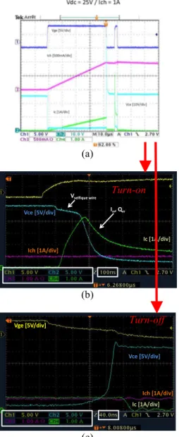
Figure 10a shows a permanent buck-mode on the scope screen at low current operation due to the absence of heat sink. In Figure 10a a greater load current can be obtained by means of a low frequency "double pulsed" method whose typical waveforms are recalled in Figure 10a. Based on this, Figure 10b and 10c, give the obtained voltage and current waveforms on one low-side RC-IGBT die: at turn-on (recovery sequence of the high side RC-IGBT's diode) with the inductive voltage drop of the loop; and at turn-off (slight inductive over-voltage across the die). It should be noted that the current measurement was realized by means of a small Rogowski™ (20MHz) coil around a wire section and the PCB that appears as an interesting non-intrusive method for integrated converter. The correct switching time of the dies (<200ns) with low oscillations demonstrate the dynamic electrical capability of the proposed dies and the assembly approach. (a) Irr, Qrr Vselfique wire Vce [5V/div] Ic [1A/div] Ich [1A/div] (b) Vce [5V/div] Ich [1A/div] Vge [5V/div] Ic [1A/div] (c)
Figure 10: (a) Typical double-pulse waveforms produced by the set-up, (b) turn-on RC-IGBT (flip-chip die) waveforms, (c) turn-off RC-IGBT (flip-(flip-chip die) waveforms [3].
Stray inductance – Measurement results
Two prototypes of H-bridge converter have been designed and the first stray inductance measurement results are provided.
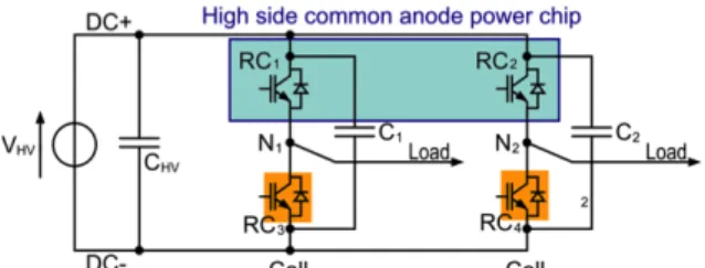
Following the previous section, Figure 11 shows the H-Bridge converter with a five-die configuration with a similar implementation to the previous three-die configuration. Indeed, the high-side die is a three-pole common anode RC-IGBT (blue in the schematic) but the two low-side RC-IGBTs have been replaced by the association of two flip-chip IGBT dies (gray) and two diode dies (red). As shown in Figure 12, the IGBT stray inductance (red area) is orthogonal to the PCB plan [4][6] and is equal to the diode stray inductance (green area) because the common anode chip is placed between the other chips. This loop exhibits a lower stray inductance than a planar classic loop. The results obtained in this section can be extended to the three-die configuration by using an RC-IGBT instead of the IGBT. 1 C VHV HV RC 1 1 N1
High side common anode power chip
DC+ DC-D IGBT C1 Load 2 RC 2 2 N2 D IGBT C2 Load Cell1 Cell2 (a) RC N D IGBT C Load DC+ DC-m,Diode Cellm m m m m RC N D IGBT C Load DC+ DC-m,IGBT Cellm m m m m Power loop IGBT Lloop IGBT
Power loop Diode Lloop Diode
(b)
Figure 11: (a) Electrical circuit (five-die configuration) and (b) details on stray inductance.
DC-DC+ VG,RC1 VG,RC2 VG,IGBT1 VG,IGBT2 D2 D1 IGBT1 IGBT2 N1 N2 Lloop IGBT
High side common anode power chip RC1 RC2 Lloop Diode Load Load CDiode CIGBT (a) Turn-on Turn-off
Lloop IGBT Lloop Diode
(b)
Figure 12: Proposed H-bridge (5 dies) circuit and illustration of the orthogonal loop: (a) top view and (b) side view.
A conventional H-bridge is used in order to compare the measurement results to those of the proposed solution (Fig. 13). Four RC-IGBTs are used and the lateral power loop is illustrated in Figure 14. RC RC C1 1 N1 3 Load RC C2 2 N2 4 Load C VHV HV DC+ DC- Cell1 Cell2 RC Power loop Lloop 2 Lloop 1
Figure 13: Conventional H-bridge (4 dies) - Electrical circuit. VG,RC1 VG,RC2 DC+ DC-RC1 RC2 RC3 RC4 N1 N2 VG,RC3 VG,RC4 Load C2 Lloop 2 Lloop 1 C1
Figure 14: Conventional H-bridge and top-view of the planar loop.
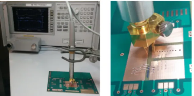
An Agilent 4294A impedance analyzer is used to measure the stray inductance as shown in Figure 15 [7]. The two PCB are 35µm Cu substrate. Measurements are realized with 250µm Al wire bonding.
Figure 15: Experimental measurement with the impedance analyzer used with a special PCB probe.
The solution that we propose, presents a stray inductance area which is approximately 4 times lower than the conventional design leading to lower
stray inductances. Results in Table 1 are given at 1MHz and 10 MHz. The assembly of the three-pole common-anode and two low side flip-chip RC-IGBTs reduces significantly the stray inductance.
Table 1: Measurements of the stray inductance for the conventional and proposed design for 3, 2 and 1 wire bonding (WB).
Ls - nH Conventional Proposed 1MHz 10MHz 1MHz 10MHz 3WB 10.97 10.78 4.66 4.54 2WB 12.11 12.03 5.43 5.29 1WB 16.43 15.88 8.13 7.72 Conclusion
The paper deals with the integration of a generic power converter (DC/AC or AC/DC). The aim of this integration approach is to suppress wire bonds and to have a compact package in order to improve electrical performance as well as reliability of the power modules in medium power applications. To that end, the integration approach combines both monolithic integration in silicon and hybrid integration on a PCB/DBC substrate. The approach presented in the paper is the « two chip » approach that integrates a multi-phase converter within two complementary multi-pole power chips named common anode and common cathode power chips.
The approach is validated in an H-bridge
converter through SentaurusTM 2D numerical
simulations as well as experimental
characterizations. Indeed, the common anode multi-pole chip is realized and characterized alone. Then, it is assembled on a PCB substrate with two RC-IGBT chips (partial flip-chip assembly) to realize the
H-bridge. First experimental electrical
characterization validated the operating modes of the H-bridge converter. Specific stray inductance measurements of the commutation loop using an impedance analyzer showed that its value is highly reduced, as compared to the conventional one.
Acknowledgements
«This research work received financial support from the National Research Agency (ANR). The project name is "ConvPlUS", ANR-13-JS09-0008-01»
References
[1] A. El khadiry, A. Bourennane, M. Breil, F. Richardeau, "Monolithically integrated switching cells suitable for high density power conversion", International Seminar on Power Semiconductors (ISPS 2012), Prague (République Tchèque), 29-31 Août 2012, pp.222-229, N° 12311.
[2] A. El khadiry, F. Richardeau, A. Bourennane, D. Zhifeng, M. Breil, "Multi-switch Si-chip structures and on-substrate packaging techniques for improving the electrical performance of power modules", European Conference on Power
Electronics and Applications (EPE), Lille (France), Septembre 2013, p. 7, N° 13285.
[3] A. El khadiry, A. Bourennane, F. Richardeau, A. Lale, S. Charlot, "Monolithic multi-pole converter device for medium power applications" European Conference on Power Electronics and Applications (EPE), Lappeenranta (Finlande), Août 2014, p. 7, N° 14451.
[4] A. Lale, N. Videau, A. Bourennane, F. Richardeau, "Analysis of the three-chip switching cells approach for integrated multi-phase IGBT-based power converter " European Conference on Power Electronics and Applications (EPE), Geneva (Switzerland), September 2015 (accepted).
[5] K. Takahashi et al., "1200V Class Reverse Conducting IGBT optimized for Hard
Switching Inverter", PCIM Europe 2014,
Nuremberg, Germany.
[6] N. Videau, "Convertisseurs continu-continu non isolés à haut rapport de conversion pour Piles à Combustible et Electrolyseurs - Apport des composants GaN", PhD Dissertation, Institut National Polytechnique de Toulouse (INPT), Laboratoire Laplace, Toulouse, France, 2014.
[7] Shengnan Li; Tolbert, L.M.; Wang, F.; Fang Zheng Peng, "Reduction of stray inductance in power electronic modules using basic switching cells," Energy Conversion Congress and Exposition (ECCE), 2010 IEEE, vol., no., pp.2686-2691, 12-16 Sept. 2010.
![Figure 1: Illustration of the proposed « two-chip » multi-pole integration approach [1-2]](https://thumb-eu.123doks.com/thumbv2/123doknet/14426107.514236/3.892.203.694.156.311/figure-illustration-proposed-chip-multi-pole-integration-approach.webp)