HAL Id: lirmm-02079679
https://hal-lirmm.ccsd.cnrs.fr/lirmm-02079679
Submitted on 13 May 2019
HAL is a multi-disciplinary open access
archive for the deposit and dissemination of
sci-entific research documents, whether they are
pub-lished or not. The documents may come from
teaching and research institutions in France or
abroad, or from public or private research centers.
L’archive ouverte pluridisciplinaire HAL, est
destinée au dépôt et à la diffusion de documents
scientifiques de niveau recherche, publiés ou non,
émanant des établissements d’enseignement et de
recherche français ou étrangers, des laboratoires
publics ou privés.
Design and Evaluation of a 28-nm FD-SOI STT-MRAM
for Ultra-Low Power microcontrollers
Guillaume Patrigeon, Pascal Benoit, Lionel Torres, Sophiane Senni, Guillaume
Prenat, Gregory Di Pendina
To cite this version:
Guillaume Patrigeon, Pascal Benoit, Lionel Torres, Sophiane Senni, Guillaume Prenat, et al.. Design
and Evaluation of a 28-nm FD-SOI STT-MRAM for Ultra-Low Power microcontrollers. IEEE Access,
IEEE, In press, 7, pp.58085-58093. �10.1109/ACCESS.2019.2906942�. �lirmm-02079679�
Date of publication May 10, 2019, date of current version May 13, 2019.
Design and Evaluation of a 28-nm FD-SOI
STT-MRAM for Ultra-Low Power
microcontrollers
Guillaume Patrigeon1 , Pascal Benoit1 , Lionel Torres1 , Sophiane Senni1 , Guillaume Prenat2 , Gregory Di Pendina2
1LIRMM - Université de Montpellier, CNRS - France - firstname.lastname@lirmm.fr 2SPINTEC - Université Grenoble-Alpes, CNRS, CEA - France - firstname.lastname@cea.fr Corresponding author: Guillaume Patrigeon (e-mail: guillaume.patrigeon@lirmm.fr).
This work has received funding from the European Union’s Horizon 2020 research and innovation program under grant agreement No 687973 (GREAT project) and the French National Research Agency under grant ANR-15-CE24-0033-01 (MASTA project).
ABSTRACTThe complexity of embedded devices increases as today's applications request always more services. However, the power consumption of systems-on-chip has significantly increased due to the high-density integration and the high leakage power of current CMOS transistors. To address these issues, emerging technologies are considered. Spin-Transfer Torque Magnetic Random Access Memory (STT-MRAM) is seen as a promising alternative solution to traditional memories thanks to its negligible leakage current, high density, and non-volatility. In this work, we present the design and evaluation of a 128 kB STT-RAM in 28-nm FD-SOI technology with SSTT-RAM-like interface for ultra-low power microcontrollers. With 0.9 pJ/bit read in 5 ns and 3 pJ/bit write in 10 ns, this embedded non-volatile memory is suitable for devices that run at frequencies under 100 MHz. Considering low-power application with duty-cycled behaviour, we evaluate the STT-MRAM as a replacement of embedded Flash and SRAM by comparing single and multi-memory architecture scenarios.
INDEX TERMS28-nm FD-SOI, microcontroller, STT-MRAM, Ultra-Low-Power
I. INTRODUCTION
Nowadays, embedded systems are widely used in various domains, and many applications set high constraints for designers and developers in terms of performance and energy consumption. However, while the complexity of embedded devices is continuously increasing, the power consumption of systems-on-chip is a challenge for battery-powered applications. Having long autonomy for such devices becomes a real need. The energy consumption of an Ultra-Low Power (ULP) microcontroller can be optimised at multiple levels. A lot of ULP applications have a periodic behaviour, alternating between run and sleep phases (“duty-cycle” operation mode, Figure 1 (a)). The time spent in each phase depends on the application specifications and selected solutions. Even though sleep modes help to reduce the power consumption of a microcontroller, some energy is still lost during sleep phases. As a workaround, it is possible to power down a microcontroller during sleep phases (Figure 1 (b)),
but for traditional architectures the system state is then lost, forcing a system reboot. Another solution is to insert Non-Volatile Logic (NVL) inside the architecture to make it able to store its state before a shut down, and restore it after wake-up (normally-off computing, Figure 1 (c)). State recovery by using NVL is faster and more energy efficient than a full restart [1], but this solution adds an overhead in terms of area and makes the go-to-sleep phase time longer. This method also requires some energy to store the system state and restore it at wake-up. Comparing the traditional microcontroller with the normally-off solution, there is a trade-off between the energy lost in sleep phase (Figure 1 (a)) and the backup energy overhead (Figure 1 (c)).
Different approaches are studied to achieve the lowest power consumption for ULP applications. NVL is used to powering down parts of a system logic by saving its state into non-volatile registers, and then avoiding the leakage current during sleep phases (Figure 1 (c)). [2] integrates non-volatile
G. Patrigeon et al.: Design and Evaluation of a 28-nm FD-SOI STT-MRAM for Ultra-Low Power microcontrollers
cells directly into flip-flops, managed by a dedicated controller, whereas [1] and [3] use non-volatile arrays outside logic to save the system state. Depending on the applications, some state of the art solutions focus more on reducing active energy consumption than on removing sleep leakage power. [4] and [5] use body-biasing methods to achieve lower active energy and [6] adapts their memory architecture. However, because the size of memories used by [6] is very small (2x 1 kB), the solution is dedicated to a limited number of applications. Moreover the microcontrollers from [6] and [4] require to be initialized from an external device to obtain their program, which adds constraints to their integration in embedded devices. [1], [5] and [3] use an architecture and memory sizes similar to commercial products (Table 2), with non-volatile memory and a SRAM. Only [2] is based on a single non-volatile memory architecture, the other works presented in Table 1 separate application's program and data in different
memories. Moreover, [2] uses only non-volatile memories. That solution helps to reach the lowest energy consumption in sleep mode without performing data transfers to save the content of volatile parts.
[1], [2] and [3] use Ferroelectric memories when non-volatility is needed. Here we use another kind of NVM technology: STT-MRAM. Spin-Transfer Torque Magnetic Random Access Memory (STT-MRAM) is seen as a promising alternative solution to traditional memories thanks to its negligible leakage current, high density, and non-volatility. By combining the 28-nm FD-SOI technology for CMOS and STT-MRAM solution for the memory system, we investigate the different architectural solutions to improve the energy efficiency, reliability, and performances of systems-on-chip for ULP applications. In comparison to FeRAM, STT-MRAM offers lower access latencies, higher retention and density ([13], [14]). In this work, we focus on
(a) Sleep mode (b) Power down mode (c) Normally-off computing
FIGURE 1. Duty-cycle mode operation
TABLE 1. Ultra-Low-Power microcontrollers
Lallement 2018 [4] Lin 2018 [6] Zwerg 2017 [1] Izumi 2015 [2] Singhal 2015 [5] Khanna 2014 [3]
Technology 28 nm FD-SOI 180 nm 130 nm 130 nm 90 nm 130 nm HVT
Power supply - 0.2V-1.1V 1.2V/1.5V 1.2V/3.0V 3V 1.5V
Frequency 16 MHz - 8 MHz 24 MHz 16 MHz 8 MHz
CPU Cortex-M0+ MSP430 Cortex-M0+ Cortex-M0 MSP430 32-bit
Memory architecture 4 kB SRAM (code) 4 kB SRAM (data) 128 B ROM (boot) 1 kB latch (code) 1 kB latch (data) 96 kB ROM 2x 32 kB FRAM 2 kB SRAM Non-Volatile Array 16 kB 6T4C NVRAM (code and data) Non-Volatile Logic (Ferroelectric NVFF) 64 kB NVRAM 8 kB SRAM MTCMOS FF 10 kB ROM 64 kB FRAM 8 kB SRAM Non-Volatile FeCap Array
Active power 2.7 pJ/cycle 33 pJ/cycle @ 0.45V 150 µA/MHz @ 1.2V 6.14 µA 28.3 µW/MHz 75 µW/MHz
Sleep power 0.7 µW @ 0.5V - NVL sleep: 0 W - 0.32 µW @ 3V Retention: 0.28 µW
Sleep: 0W
Wake-up - - 380 nC, 438 µs - - 2.4 nJ, 384 ns (125 MHz)
Backup - - - 7.2 nJ, 320 ns (125 MHz)
TABLE 2. Commercial microcontrollers for low power applications STM32L0 series [7] STMicroelectronics STM32F0 series [8] STMicroelectronics LPC1100 series [9] NXP Semiconductors nRF51 series [10] Nordic Semiconductors PSoC 4 family [11] Cypress Semiconductors FM0+ family [12] Cypress Semiconductors Frequency 32 MHz 48 MHz 50 MHz 32 MHz 48 MHz 40 MHz
CPU ARM Cortex-M0+ ARM Cortex-M0 ARM Cortex-M0
ARM Cortex-M0+ ARM Cortex-M0
ARM Cortex-M0
ARM Cortex-M0+ ARM Cortex-M0+
Memory architecture Flash 8 to 192 kB SRAM 2 to 20 kB EEPROM 512 to 6144 B Flash 16 to 256 kB SRAM 4 to 32 kB Flash 4 to 256 kB SRAM 2 to 36 kB EEPROM 512 to 4096 B Flash 128 to 256 kB SRAM 16 to 32 kB Flash 8 to 256 kB SRAM 2 to 32 kB Flash 56 to 88 kB SRAM 6 kB
the memory architecture and memory technologies for ULP devices. An overview of memory architecture solutions is introduced in Section II. Section III presents the design of an embedded 1kB perpendicular peSTT-MRAM with 28-nm FD-SOI CMOS, whose evaluation is detailed in Section IV. Finally, Section V concludes this paper and provides future directions for research works.
II. MEMORY ARCHITECTURE OVERVIEW
A. MICROCONTROLLER ARCHITECTURE
The specifications of an application determine which microcontroller to use. Manufacturers generally offer a large variety of microcontrollers to answer to the large number of actual embedded applications and their specific constraints, as it is not possible to create one microcontroller architecture that will fit all applications. There are microcontrollers with different packages, number of input/output pins, different processors, operating frequencies, peripherals, communication interfaces, analogic modules, low-power modes, memory technologies, memory capacities, and dedicated to different kinds of applications (automotive for example). However, there are some similarities between all these different devices. Typical microcontrollers include at least one processor, a non-volatile memory (usually Flash for
code instructions and read-only data), a volatile memory (usually SRAM for application data), a power management unit, a clock management unit, input/output peripherals, communication modules (UART, SPI, I2C, USB, CAN…) and timers. This typical architecture is depicted in Figure 2. Some microcontrollers also include different types of non-volatile memories (ROM, EEPROM...) or have a multi-master system (multi-processor, Direct Memory Access (DMA)...).
B. MEMORY PARTINIONING
The memory architecture of microcontrollers is constrained by the architecture of the processor. With processors having a single bus interface (like the ARM Cortex-M0), it is possible to store both code and application data in the same memory without affecting the performances of the system. Some other processors (like the ARM Cortex-M3) have multiple bus interfaces (for instruction, data, system…) and require dedicated memory architectures: as they are able to handle parallel transactions, having a single memory architecture with a single access bus decreases the overall system performances. Multi-master systems (when using specific modules like DMA) are also affected by the number of interfaces of the main memories.
ARM Cortex-M architecture is widely used in commercial low-power microcontrollers and we use one of its implementation that is available for academic projects in our evaluation: the ARM Cortex-M0 r1p0. This is a 3-stage 32-bit RISC processor that implements the ARMv6-M ISA, with a maximum frequency of 50 MHz. It includes a single AHB-Lite interface, 32 interrupt lines, 1 Non-Maskable Interrupt and a single-cycle multiplier.
In this study, we focus on memory architectures for a single master system (which is the Cortex-M0, with a single bus interface). As STT-MRAM is a non-volatile random access memory, it could be used to replace both Flash for code memory and SRAM for dynamic data memory. To evaluate the possible gains by using STT-MRAM, we FIGURE 2. Typical microcontroller architecture
G. Patrigeon et al.: Design and Evaluation of a 28-nm FD-SOI STT-MRAM for Ultra-Low Power microcontrollers
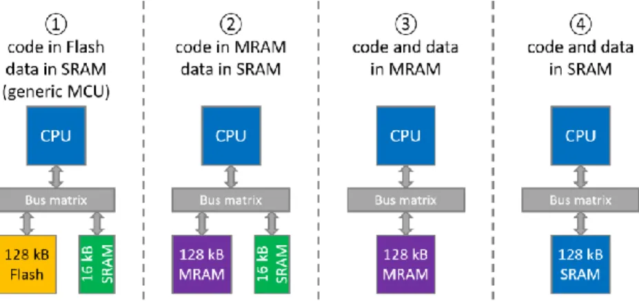
compare different memory architectures, as illustrated in Figure 3: ① program code in Flash and dynamic data in SRAM (this is actually the architecture used in most of commercial microcontrollers), ② Flash is replaced by STT-MRAM, ③ both program code and data are located in a single STT-MRAM, and ④ both program and data are located in a single SRAM.
The memory architecture of commercial low power microcontrollers using an ARM Cortex-M0 or an ARM Cortex-M0+ is in many cases composed of at least a Flash memory and a SRAM. The microcontroller families presented in Table 2 have 4 kB to 256 kB of Flash and 2 kB to 36 kB of SRAM. Regarding these capacities, we chose a main memory of 128 kB and an optional second memory of 16 kB for our evaluation.
III. MEMORY DESIGN
This section presents the design of the 128 kB (1 Mb) peSTT-MRAM with 28-nm FD-SOI CMOS.
A. SPECIFICATIONS
This memory is used as main memory for different architecture scenarios presented in Section II. To be compliant with these architectures, the memory has a single port synchronous 32-bit wide SRAM-compatible interface. The chosen CMOS technology used is the 28-nm FD-SOI from STMicroelectronics. To help identifying the memory specifications with a 28-nm technology node, two versions of memory array implementation have been considered, for
High-Performance (HP) or High-Density (HD) applications, and the performance extrapolated for different sizes and options of the memory in a compiler-oriented approach (Table 3). As our system is limited to 50 MHz by the processor, a HD architecture is preferred. For this work we have focused on the parameters of [18] and used them to define the following specifications of the bit cell: 1 transistor 1 junction architecture (1T-1MTJ), 40 nm diameter MTJ with a parallel resistance (Rp) of 1 kΩ and a minimum TMR of 150%, 10 years retention with 1012 write endurance. All the specifications of the bit cell and the memory are summarized in Table 4.
TABLE 4. Specifications of the MRAM
MTJ 40 nm
TMR, Rp, δ ≥ 150 %, 1 kΩ, 5 %
Retention 10 years
Endurance ≥ 1012
Critical current (Ic) 40 ~ 100 µA
Density 128 kB (1 Mb)
Timing 20 ~ 100 ns (10 ~ 50 MHz)
IO width 32
Bit cell size Min MOS size: 0.0364 µm2
Bit cell architecture 1T-1MTJ
Optimization techniques
Body bias Quasi differential sensing Source Line (SL) sharing
CMOS 28-nm FDSOI
Power supply 1.0 VDC
TABLE 3. STT-MRAM demonstrators for High Performance (HP) and High Density (HD) Toshiba [15] TED 2017 (HP) Toshiba [16] ISSCC 2016 (HP) Toshiba [17] ISSCC 2015 (HP) Samsung [18] IEDM 2016 (HD) Qualcomm/TDK [19] IEDM 2015 (HD)
CMOS 20 nm 65 nm 65 nm 28 nm LPP 40 LP, 6 metal levels
Density - 4x 1 Mb 1 Mb 8 Mb 1 Mb Cell architecture 2T2MTJ (L2), 1T1MTJ (L3) 2T2MTJ 2T2MTJ 1T-1MTJ (Cu backend) 1T-1MTJ (MTJ between M4 M5)
Unit cell size 3x Minsize - - 0.0364 µm² 40 F², 0.065 µm²
MTJ 16-43 nm - 47 nm 38-45 nm -
TMR, Rp, σ > 150% - -
Rp ~1 kΩ, TMR 180% for high yield @85°C
(Sensing marge 25 σ Rp variation 7%) TMR 110%, Rp ~2 kΩ (18 σ read windows) Retention Endurance 10 12 - - 10 years @ 85°C Up to 108 cycles > 1013 (10 ns Wpulse) Timing Wpulse 1-3 ns @ Ic =40-100µA Read 3.3 ns @ 1.25V (F = 300 MHz) 40 MHz Wpulse 25 ns @ 1.2V Wpulse 15 ns @ 1.5V 50 MHz ReadAccess 16 ns (0-70°) WriteAccess 20-100 ns, IO width - - - x32/x64 x32/x64 Optimization, Redundancy, Repair, ECC - Physically eliminated read disturbance write-verify-write, read-modify-write
Hierarchical bit line for eliminating disturbance
Rows and columns (activated)
Rows and columns (not activated) Power supply
(core/IO) -
1.2V, local and global power gating
1.2V, local and global
power gating 1.0V / 1.8V 1.2V / 1.8V
Error bit count WER < 6 (4 ns, 62 µA)
B. MEMORY ARCHITECTURE
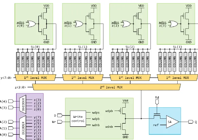
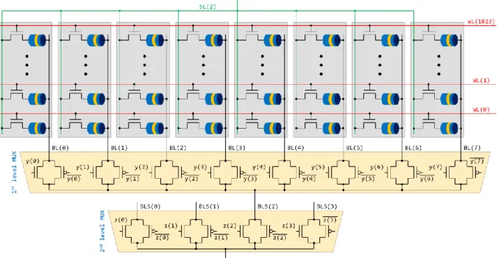
The memory is made of a single bank. The data are 32-bit wide, so the memory architecture is made of 32 IO blocks (Figure 4). Each IO contains 32 columns, 1 reference column, the reading/writing circuits and a 32 to 1 multiplexing stage is used to select the addressed column as depicted in Figure 5 and Figure 6.
C. DESIGN AND CHARACTERISATION
Based on these specifications, the memory was fully designed in a memory compiler approach, allowing to easily providing memories of different sizes according to the requirements of the application (up to 128 kB). The memory has been fully characterized at circuit level, using the electrical simulators Spectre and Ultrasim. Summarized in Table 5, one IO block requires 0.9 pJ to read the farthest bit FIGURE 4. Memory architecture, made of a single bank
FIGURE 5. Architecture of one IO block, containing 32 columns (grey), read (blue) and write (green) circuitry and a 2-level multiplexer (yellow). The column decoder (purple) is shared between IOs.
G. Patrigeon et al.: Design and Evaluation of a 28-nm FD-SOI STT-MRAM for Ultra-Low Power microcontrollers
in 5 ns (worst path case) and 3.0 pJ to write it in 10 ns, which sets the maximum operating frequency without wait states to 100 MHz. Since the simulation of a memory of such a size at circuit level is almost impossible due to huge simulation times and amount of data, the global operation of the memory was performed on very short durations and with a degraded level of accuracy for Ultrasim. The full characterization was made using the critical path of the memory, with parasitic capacitances and resistances of the access lines calculated using the Design Rules Manager (DRM) of the technology. Following a standard compiler approach, the simulations were performed for different sizes of the memory, so that the performance for a given size can be extrapolated.
TABLE 5. Memory performances
Leakage 352 µA (352 µW)
1 bit read energy 0.9 pJ
1 bit write energy 3.0 pJ
Read latency 5 ns (200 MHz max)
Write latency 10 ns (100 MHz max)
Looking at area, the 128 kB peSTT-MRAM is about 58 000 µm2. This is around 3.5 times smaller than a SRAM of the same capacity (around 204 000 µm2).
IV. EVALUATION
A. SYSTEM DETAILS
The system is kept as simple as possible to focus the evaluation on the memory architecture. The Cortex-M0 and the memories are organized around a single master AMBA3 AHB-Lite bus architecture. Here are the assumptions for this evaluation:
The maximum operating frequency is chosen to perform each memory operation in one cycle.
Both SRAM and STT-MRAM support 8-bit, 16-bit and 32-bit write operations.
Each read operation is 32-bit wide. There is no interrupt, exception nor event.
There is no shadow memory operation (single master). The energy of the matrix bus and memory controllers are not included in this work. The software benchmark used is the ULPMark from EEMBC [20]. CoreProfile (ULPMark-CP) is an application designed to reproduce a periodic behaviour with active and sleep phases (see Figure 1 (a)). The active phase of the CoreProfile is composed of math functions (linear approximation, filtering), conversion tables, string search, table copy, sorting, data permutations and output toggling. This application code is mostly used to evaluate and compare the energy efficiency of Ultra-Low-Power microcontrollers for Internet of Things applications.
A comparison of the memories in terms of power consumption and energy per operation is summarized in Table 6. The energy consumption of the SRAM comes from FIGURE 6. Columns and bit cells organization in the memory
a 128 kB memory implementation in 28-nm FD-SOI from STMicroelectronics, the read energy of the 28-nm Flash memory is extrapolated from the data of [21] and the data of the STT-MRAM are based on the results presented in Section III. If the STT-MRAM has a bigger writing energy cost (3.0 pJ/bit) than SRAM (0.73 pJ/bit) for the same capacity (128 kB), it has the lowest energy cost for read operations. As we lack information about leakage, the evaluation of the active phase only takes into account the dynamic energy.
TABLE 6. Energy cost per operation for each memory
Flash 128 kB STT-MRAM 128 kB SRAM 128 kB Operation 32-bit read 39.4 pJ 29 pJ 30.6 pJ 8-bit write - 24 pJ 5.85 pJ 16-bit write - 48 pJ 11.7 pJ 32-bit write - 96 pJ 23.4 pJ B. RESULTS
For each architecture scenario, the active phase of the application executes in 49767 cycles (32773 instructions executed). Table 7 shows the total count of the different memory operations in the code memory (that is, the location where read-only data and program code are stored) and the data memory (volatile data). Because the program code is located in the code memory, no instruction fetch occurs in the data memory, but writes operations only occur in the data memory. One instruction fetch corresponds to a 32-bit read.
TABLE 7. Memory operations for one CoreProfile active phase (49767 cycles, 32773 executed instructions)
Code memory Data memory
Idle cycles 29532 38280 Instruction fetches 18693 0 Total reads 1542 8151 Total writes 0 3336 8-bit writes 0 1000 16-bit writes 0 516 32-bit writes 0 1820
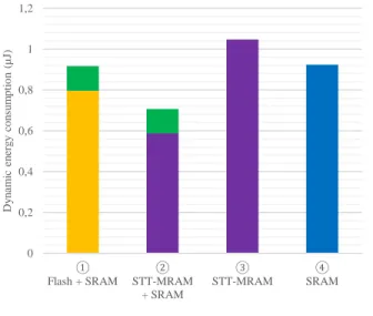
Figure 7 shows the estimated dynamic energy consumption of the memories, for the different architectures previously described in Figure 3. Each memory is represented by a different colour to distinguish its contribution.
For scenarios ① and ②, where code and data are separated in two different memories, and where only read operations are performed into non-volatile memories, we observe that the dynamic energy consumption of the
STT-MRAM is lower than the Flash's one (around 26%). As the data memories are the same for both scenarios (16 kB SRAM), their contribution is equal. In total, the memories' dynamic energy consumption for the second scenario is lower than for the first one (around 23%). For scenarios ③ and ④, where a single memory is used for both code and data, we observe that the single SRAM based architecture consumes a little bit less energy than the single STT-MRAM based architecture (around 12%), because of the higher write energy needs of the STT-MRAM. Memory operations in the 16 kB SRAM (which is used for application data only) requires less energy than in the larger memories (128 kB SRAM and STT-MRAM), that is why scenarios ③ and ④ (with a single memory architecture) have higher dynamic energy consumption than scenario ② (with separated memory architecture).
FIGURE 7. Dynamic energy consumption of the memories
Looking at power consumption in sleep mode, scenario ③ is the only one where the memory can be powered-down without losing data. Each other scenario requires keeping the volatile memory into retention state: 879 nW for scenarios ① and ②, 13.3 µW for scenario ④. Moreover, a SRAM's retention state requires keeping a dedicated voltage regulator enabled, which adds another energy cost. For scenarios ① and ②, it is possible to save its content into the non-volatile part and restore it at wake-up, but this operation takes time and energy, especially for the Flash memory in scenario ①. Finally, for scenario ④, the application code has to be loaded into SRAM from a non-volatile memory or an external source after each power up.
Now considering duty cycled behaviour (Figure 1), we can evaluate the minimum sleep period required in scenario ③, which as the lowest leakage power, to compensate the
0 0,2 0,4 0,6 0,8 1 1,2 ① Flash + SRAM ② STT-MRAM + SRAM ③ STT-MRAM ④ SRAM D y n am ic en er g y con su m pt io n ( µ J)
G. Patrigeon et al.: Design and Evaluation of a 28-nm FD-SOI STT-MRAM for Ultra-Low Power microcontrollers
overhead energy consumption compared to scenarios ① and ② in active phase. After 148 ms, the energy saved during sleep phase in scenario ③ compensate its 130 µJ overhead compared to scenario ① in active mode. After 386 ms, the single STT-MRAM memory architecture of scenario ③ is more energy efficient than the STT-MRAM + SRAM architecture of scenario ②.
In terms of flexibility, scenario ③ and ④ are the most interesting because these solutions offer the possibility to adjust the allocated memory size between application code and data. Moreover, these architectures are simpler than solutions ① and ②.
V. CONCLUSION
We have designed a 128 kB (1 Mb) peSTT-MRAM, 28-nm FD-SOI CMOS with single 32-bit port SRAM-like interface for low-power embedded application. With 0.9 pJ/bit read in 5 ns and 3 pJ/bit write in 10 ns, this embedded non-volatile memory is suitable for low-power devices that run at frequencies under 100 MHz. We presented the evaluation of STT-MRAM, SRAM and Flash solutions for different memory architectures (single and multiple memories architectures). STT-MRAM is a more interesting solution than Flash, thanks to a lower read energy (26% gain). Moreover, it has a faster, more flexible and more energy efficient write capability than traditional embedded Flash. When used as the sole memory of a system, the non-volatility of MRAM helps to reach the lowest power consumption in sleep mode, although this solution (one STT-MRAM for both code and data) is not the best for active mode. There is a trade-off between low power consumption in sleep mode and in active mode. In order to improve this study including the other parts of the system, we plan future works about the integration and evaluation of MRAM at various level, for duty-cycled ULP application.
REFERENCES
[1] M. Zwerg, S. Khanna, and S. Bartling, “Non-volatile logic SoC with software-hardware co-design and integrated supply supervisor for energy harvesting applications,” 2017, pp. 887–889.
[2] S. Izumi et al., “Normally Off ECG SoC With Non-Volatile MCU and Noise Tolerant Heartbeat Detector,” IEEE Trans. Biomed. Circuits Syst., vol. 9, no. 5, pp. 641–651, Oct. 2015.
[3] S. Khanna, S. C. Bartling, M. Clinton, S. Summerfelt, J. A. Rodriguez, and H. P. McAdams, “An FRAM-Based Nonvolatile Logic MCU SoC Exhibiting 100% Digital State Retention at VDD = 0 V Achieving Zero Leakage With <400-ns Wakeup Time for ULP Applications,” IEEE J. Solid-State Circuits, vol. 49, no. 1, pp. 95–106, Jan. 2014.
[4] G. Lallement, F. Abouzeid, M. Cochet, J.-M. Daveau, P. Roche, and J.-L. Autran, “A 2.7 pJ/cycle 16 MHz, 0.7 µW Deep Sleep Power ARM Cortex-M0+ Core SoC in 28 nm FD-SOI,” IEEE J. Solid-State Circuits, vol. 53, no. 7, pp. 2088–2100, Jul. 2018.
[5] V. K. Singhal, V. Menezes, S. Chakravarthy, and M. Mehendale, “A 10.5uA/MHz at 16MHz single-cycle non-volatile memory
access microcontroller with full state retention at 108nA in a 90nm process,” 2015, pp. 1–3.
[6] L. Lin, S. Jain, and M. Alioto, “A 595pW 14pJ/Cycle microcontroller with dual-mode standard cells and self-startup for battery-indifferent distributed sensing,” 2018, pp. 44–46. [7] “STM32L0 - ARM Cortex-M0+ ultra-low-power MCUs -
STMicroelectronics.” [Online]. Available:
https://www.st.com/en/microcontrollers/stm32l0-series.html?querycriteria=productId=SS1817. [Accessed: 22-Oct-2018].
[8] “STM32F0 - ARM Cortex-M0 Microcontrollers - STMicroelectronics.” [Online]. Available:
https://www.st.com/en/microcontrollers/stm32f0-series.html?querycriteria=productId=SS1574. [Accessed: 22-Oct-2018].
[9] “LPC1100 Series: Scalable Entry-level Microcontrollers (MCUs) based on Arm® Cortex®-M0+/M0 Cores|NXP.” [Online]. Available: https://www.nxp.com/products/processors-and- microcontrollers/arm-based-processors-and-mcus/lpc-cortex-m-mcus/lpc1100-cortex-m0-plus-m0:MC_1392389687150. [Accessed: 22-Oct-2018].
[10] “Low power short-range wireless products - Nordic
Semiconductor.” [Online]. Available:
https://www.nordicsemi.com/en/Products/Low%20power%20short -range%20wireless. [Accessed: 15-Apr-2019].
[11] “32-bit Arm® Cortex®-M0 PSoC® 4.” [Online]. Available: http://www.cypress.com/products/32-bit-arm-cortex-m0-psoc-4. [Accessed: 22-Oct-2018].
[12] “ARM Cortex M0+ FM0+.” [Online]. Available: http://www.cypress.com/products/fm0-32-bit-arm-cortex-m0-microcontroller-mcu-families. [Accessed: 22-Oct-2018].
[13] J. Meena, S. Sze, U. Chand, and T.-Y. Tseng, “Overview of emerging nonvolatile memory technologies,” Nanoscale Res. Lett., vol. 9, no. 1, p. 526, 2014.
[14] L. Cargnini, L. Torres, R. Brum, S. Senni, and G. Sassatelli, “Embedded Memory Hierarchy Exploration Based on Magnetic Random Access Memory,” J. Low Power Electron. Appl., vol. 4, no. 3, pp. 214–230, Aug. 2014.
[15] D. Saida et al., “1X- to 2X-nm perpendicular MTJ Switching at Sub-3-ns Pulses Below 100 µA for High-Performance Embedded STT-MRAM for Sub-20-nm CMOS,” IEEE Trans. Electron Devices, vol. 64, no. 2, pp. 427–431, Feb. 2017.
[16] H. Noguchi et al., “4Mb STT-MRAM-based cache with memory-access-aware power optimization and write-verify-write / read-modify-write scheme,” 2016, pp. 132–133.
[17] H. Noguchi et al., “A 3.3ns-access-time 71.2uW/MHz 1Mb embedded STT-MRAM using physically eliminated read-disturb scheme and normally-off memory architecture,” 2015, pp. 1–3. [18] Y. J. Song et al., “Highly functional and reliable 8Mb STT-MRAM
embedded in 28nm logic,” 2016, pp. 27.2.1-27.2.4.
[19] Y. Lu et al., “Fully functional perpendicular STT-MRAM macro embedded in 40 nm logic for energy-efficient IOT applications,” 2015, pp. 26.1.1-26.1.4.
[20] “CPU Energy Benchmark – MCU Energy Benchmark – ULPMark – EEMBC Embedded Microprocessor Benchmark Consortium.” [Online]. Available: https://www.eembc.org/ulpmark/. [Accessed: 22-Oct-2018].
[21] I. Kouznetsov, “Embedded 28-nm Charge-Trap NVM Technology,” presented at the Flash Memory Summit 2017, Santa Clara, CA, 2017.
![TABLE 2. Commercial microcontrollers for low power applications STM32L0 series [7] STMicroelectronics STM32F0 series [8] STMicroelectronics LPC1100 series [9] NXP Semiconductors nRF51 series [10] Nordic Semiconductors PSoC 4 family [11] Cypress](https://thumb-eu.123doks.com/thumbv2/123doknet/13340978.401579/3.864.46.810.609.729/commercial-microcontrollers-applications-stmicroelectronics-stmicroelectronics-semiconductors-semiconductors-cypress.webp)