HAL Id: hal-02463801
https://hal.archives-ouvertes.fr/hal-02463801
Submitted on 26 Feb 2020
HAL is a multi-disciplinary open access
archive for the deposit and dissemination of
sci-entific research documents, whether they are
pub-lished or not. The documents may come from
teaching and research institutions in France or
L’archive ouverte pluridisciplinaire HAL, est
destinée au dépôt et à la diffusion de documents
scientifiques de niveau recherche, publiés ou non,
émanant des établissements d’enseignement et de
recherche français ou étrangers, des laboratoires
Controlling the shape of a tapered nanowire: lessons
from the Burton-Cabrera-Frank model
E. Bellet-Amalric, Régis André, C. Bougerol, M. den Hertog, Ali Jaffal, Joël
Cibert
To cite this version:
E. Bellet-Amalric, Régis André, C. Bougerol, M. den Hertog, Ali Jaffal, et al.. Controlling the shape
of a tapered nanowire: lessons from the Burton-Cabrera-Frank model. Nanotechnology, Institute of
Physics, 2020, 31 (27), pp.274004. �10.1088/1361-6528/ab849e�. �hal-02463801�
Controlling the shape of a tapered nanowire:
lessons from the Burton-Cabrera-Frank model
E Bellet-Amalric
1, R Andr´e
2, C Bougerol
2,
M den Hertog
2, A Jaffal
3,4, J Cibert
2,aFebruary 26, 2020
1 Univ Grenoble-Alpes, CEA, IRIG, 38000 Grenoble, France 2Univ Grenoble-Alpes, CNRS, Institut N´eel, 38000 Grenoble, France 3Univ Lyon, INSA Lyon, CNRS, INL, 69621 Villeurbanne, France 4Univ Lyon, Ecole Centrale de Lyon, CNRS, INL, 69134 Ecully, France a joel.cibert@neel.cnrs.fr
Abstract
The propagation of sidewall steps during the growth of nanowires is calculated in the frame of the Burton-Cabrera-Frank model. The stable shape of the nanowire comprises a cylinder section on top of a cone section: their characteristics are obtained as a function of the radius of the catalyst-nanowire area, the desorption-limited diffusion length of adatoms on the terraces, and the sticking of adatoms at step edges. The comparison with experimental data allows us to evaluate these last two parameters for InP and ZnTe nanowires; it reveals a different behavior for the two materials, related to a difference by an order of magnitude of the desorption-limited diffusion length.
Keywords: nanowires, steps, semiconductors, molecular beam epitaxy, electron microscopy, Burton-Cabrera-Frank model
1
Introduction
The interest of a tapered waveguide for directing the light emitted into free space by a single photon emitter such as a quantum dot (QD) has been first demonstrated thanks to structures realized by a top-down approach, by etching a GaAs wafer containing multiple InAs quantum dots [1]. Quite rapidly however, the possibility to obtain a suitable waveguide in a bottom-up process during the growth of a tapered nanowire (NW) was demonstrated by positioning a single (In,As)P QD in an InP NW [2, 3, 4]. In addition to the exact positioning of
the QD on the NW axis, this allows a further manipulation of the NW-QD ensemble in order to insert it into a photonic circuit [5, 6] in which different active components can be inserted. The efficiency of the coupling to the air or to the waveguide depends on the cone angle, with typical values of the order of a few degrees [6, 7], and typical length a few micrometers.
Growing a NW with a regular cone shape may seem a simple task, as it should be enough to adjust and control a constant ratio between the radial growth rate dR/dt and the axial growth rate dL/dt. This however involves complex entangled mechanisms, since the vapor-liquid-solid (VLS) or vapor-solid-solid (VSS) mechanism for the axial growth, and the vapor-solid mechanism for the radial growth, are fed and linked by diffusion processes. As a result, more complex shapes are experimentally observed, as for instance pencil-shaped NWs [8], or other shapes [9, 10]. Most of the theoretical studies have been devoted to quantifying the axial growth rate, with the accent put first on the diffusion processes to the droplet or nanoparticle acting as a catalyst [11]; the role of the nucleation and propagation of monoatomic steps at the liquid-solid or solid-solid interface is now well recognized and studied [12, 13, 14]. Sophisticated models have been applied to one of the simplest systems: atomistic simulations developed for the metal-covalent system [15] point to the role of facets and their variation during the growth of Si NWs [16]. The line tension at the droplet-NW interface [17, 18] determines the contact angle and hence the shape of the droplet and the size of the contact area: as a result, a modification of the NW radius may be expected during the early step of growth [19]. Turning to the radial growth, descriptions generally focus onto the nucleation on the sidewalls [9, 20, 21], although step flow is often invoked. Step dynamics has been explicitly taken into account more recently [22, 23], and examples of parameters are given which lead to a cone shape, a pencil shape, or a series of step bunches.
Here we discuss the role of step dynamics on the stabilization of a cone-shaped, tapered NW, during its growth; we examine the consequences for the actual shape of the NW, which exhibits a cylinder-shaped tip section. Analytical results are presented on the range of values which can be attained for the cone angle and the cylinder length, as well as the axial and radial growth rates. These results are applied to two different systems, InP and ZnTe, for which experimental results are available on the growth of NWs in the VLS and VSS modes respectively.
2
Experimental aspects
InP NWs grown by metal organic molecular beam epitaxy (MOMBE) display a cone shape close to the substrate, with a cylinder-shaped section between the cone and the droplet [24, 25]. The length of the cylinder depends on the NW radius [24] and has been considered to be a measure of the so-called migration length. In contrast, short InP NWs grown by solid-source molecular beam epitaxy (MBE) feature a pencil shape [7]; however longer NWs, or NWs with a shell grown at lower temperature, display a regular cone shape on top of a
cylinder section [7, 26]. Large values of the half angle θ of the cone, with tan θ up to 0.16, are obtained by decreasing the growth temperature, which decreases dL/dt while keeping dR/dt almost constant [7, 26].
Figure 1 introduces our second example, that of ZnTe NWs, grown by MBE, and observed by scanning electron microscopy (SEM) with a 65◦tilt, or
trans-mission electron microscopy (TEM): growth and observation conditions are de-scribed in Ref. [27] and [28]. The NWs shown in Fig. 1 were chosen as having a gold nanoparticle radius ∼ 5 nm (except the NW grown at 400◦C since the
nanoparticle size is larger at this temperature); all have the zinc-blende struc-ture. Taking the growth at 350◦C with stoichiometric flux as an example, the
two images and the plot of the radius-length dependance illustrate the repro-ducibility of the aspect ratio for different growth times or flux values. Such a stable character of the shape during the growth was already noticed even for more complex shapes of III-V NWs [29]. Figure 1 illustrates the possibility to adjust the cone angle by the control of the growth conditions: it will be shown below that the increase of angle value is related to a concomitant increase of the radial growth rate and decrease of the axial growth rate.
3
Model
A regular cone shape suggests the presence of a regular step array on the side-walls, and the dynamics of these steps must be taken into account. A simplified view involves well-formed (110) facets or a circular cross section. Although the actual picture certainly involves a more complex shape and some disorder, we assume that the step height is that of (110) facets, a⊥= a0/2√2 where a0is the
zinc-blende lattice parameter. We note akthe interplane distance perpendicular
to the step ledge in the terrace plane (i.e., along the NW axis), ak= a0/
√ 3. Our main assumption is the availability of steps nucleated at the basis of the NW, or in a section below the expected cone-shaped section.
The Burton-Cabrera-Frank model (BCF) [30] is commonly used to describe growth by MBE [31]. The flux of atoms creates adatoms which diffuse on terraces (as described by the diffusion coefficient D, associated to a hopping probability phop of an adatom to a neighboring site), until they desorb (with a
probability of desorption pdes and a lifetime τ =pdes1 ) or are incorporated into
the crystal when they encounter a proper nucleation center. Steps form such nucleation centers, and the simplest formulation of growth by step flow assumes a one-dimensional array of steps, separated by terraces. While these concepts have been widely used to describe the growth of two-dimensional layers, their application to the radial growth and the dynamics of steps on NW sidewalls, towards a better understanding of the shape of these NWs, is quite recent [22, 23]. In this series of papers, the sticking of adatoms at steps was assumed to be large. A final numerical calculation was performed for chosen values of the characteristic parameters describing the dynamics of steps: it allowed the authors to demonstrate the possibility of a cylinder shape with radial growth, of a ”pencil shape” due to step bunching, and of tapering [22, 23]. The nucleation
Figure 1: ZnTe NWs grown under different conditions of flux ratio (stoichiomet-ric from a ZnTe effusion cell, or adding a Te flux) and temperature (from 320◦C
to 400◦C), as indicated. The values of flux and growth times are different for
each NW (resulting for instance in a factor of about 3 in the length of the two NWs shown on the left). The NWs are observed by SEM (tilt 65◦), except for
the two central ones observed by TEM. The scale bar (200 nm) is common to all images. Insert: increase of the radius as a function of length, for NWs grown at 350◦C under stoichiometric ZnTe flux, with different values of the flux and
growth time (several NWs for each sample, with a specific symbol for a given sample); the slope gives the aspect ratio.
Figure 2: (a) Scheme of the BCF model with material parameters; the flux reaches the terraces, at an angle α with respect to the NW axis, and also contributes directly to the concentration in the nanoparticle/droplet; (b) and (c) Reduced adatom density n(x)−neq
Fατ −neq as a function of the position according
to the BCF model applied (b) to an array of regular steps, and (c) to the step array and NW tip, in both cases with values of λβτ
des and
2ls
λdes as indicated.
of steps was shown to take place at or near the basis of the NW. In the present study, we introduce the possibility of a low probability of incorporation at the steps [32], pinc, which may be much lower than the hopping probability phop at
the origin of diffusion on the terraces. We also explicitly take into account the desorption of adatoms and the sublimation of the material, two effects which are currently observed during the MBE growth of II-VI semiconductors, and were taken into account when using the BCF formalism to describe the growth of a CdTe layer [33, 34].
The material parameters relevant for the BCF model are schematized in Fig. 2 (a). A list of characteristic lengths is given in Table 1. Steps of the calculation are detailed in the appendix.
The sidewalls of the NW receive an average flux Fα = F sin α/π, where
direction and the NW axis. Note that the calibration of the flux is obtained from the growth rate on a substrate, which gives a measure of F cos α. It is quite convenient to express these fluxes in nm per unit time, corresponding to the growth rate of a thick layer of the material if every atom sticks: that means that F is the flux in atoms per unit area and unit time, multiplied by the volume Ω of the unit cell.
On a wide terrace and in the absence of nucleation, the incident flux is bal-anced by desorption, so that the adatom density (actually, the adatom density multiplied by the volume Ω of the unit cell) is n = Fατ , where pdes= 1/τ is the
probability of adatom desorption.
In its simplest formulation, growth by step flow assumes a one-dimensional array of steps, separated by terraces of length 2ls(Fig. 2a and b). The adatom
density at position x along a terrace, n(x), obeys the diffusion equation char-acterized by D and τ : the uniform solution n = Fατ is modified by adding
a combination of two exponential or two hyperbolic functions, for instance n(x) = Fατ −A cosh(x/λdes)−B sinh(x/λdes), where λdesis the diffusion length
limited by the desorption of the adatoms, λdes = √Dτ . The two coefficients
A and B are determined by the boundary conditions at the steps: if, for the sake of simplicity, we assume no Ehrlich-Schw¨obel effect [31], the symmetry im-poses B = 0 if the position is measured from the center of the terrace. The parameter A is determined by the fact that the current related to the gradient of adatoms balances the incorporation of adatoms on both sides at the step: ∓D∇n(±ls) = β[n(±ls) − neq], where the parameter β sets the efficiency of
trapping at the step [22, 35], and neq is determined by the sublimation rate
Vsub of the material, neq = Vsubτ . The sublimation process involves the
re-lease of an atom already incorporated, generally at a step edge, adding thus an adatom to the neighboring terrace [33], which then diffuses and may be desorbed or re-incorporated.
symbol parameter
2ls terrace length in the cone
l0+ ls terrace length at tip
λdes diffusion length on infinite terrace
λef f effective diff. length for axial growth rate
Table 1: Characteristic lengths used in the text A straightforward calculation leads to
n(x) − neq Fατ − neq = 1 − βτ λdes βτ λdes+ tanh( ls λdes) cosh( x λdes) cosh( ls λdes) . (1)
The incorporation of adatoms at a step induces the propagation of the step, with a velocity Vstep, and the growth of the layer, with a growth rate dhdt =
a⊥
dR
dt. From Eq.1, we obtain
dR dt = (Fα− Vsub) λdes ls βτ tanh( ls λdes)
βτ + λdestanh(λldess )
, Vstep= (Fα− Vsub) 2λdes a⊥ βτ tanh( ls λdes)
βτ + λdestanh(λldess )
. (2)
The sublimation rate of the semiconductor material (represented by Vsub
and neq in the previous equations), must be taken into account for the growth
of CdTe in the form of 2D layers [33] and NWs [36]: it results in a decrease of the growth rate when the temperature is increased. We find no such evidence that it plays a role for ZnTe and InP NWs grown under the present conditions and it will be omitted in the following.
The adatom density on a single terrace separated by two steps is plotted in Fig. 2 (b) for different values of the sticking probability. At strong stick-ing probability, the boundary condition is simply n(ls) = neq; a decrease in
the sticking efficiency is partially compensated by an increase of n(ls),
lead-ing however to a decrease of the adatom current and a decrease of the step velocity. The step velocity depends also on the terrace length 2ls. The
maxi-mum step velocity, obtained for a low density of steps and a strong sticking, is Vstep= (Fα− Vsub)2λades⊥ .
This propagation of the step on the sidewalls of a cone-shaped NW has to be compared to the (axial) growth rate of the NW. The catalyst (nanoparticle or droplet) present at the tip of the NW is often considered as a perfect trap, implying n(0) = neq at the NW tip.
In the absence of steps on the sidewalls in the vicinity of the NW tip, the adatom density is described by a simple exponential function of x/λdes; the NW
growth rate is obtained by writing that the adatom current feeds a disk of radius R at the tip of the NW, hence dLdt = (Fα− Vsub)2λRdes. This is much smaller
than the maximum step velocity Vstep= (Fα− Vsub)2λades⊥ given in the previous
paragraph. Indeed, this is one of the configurations considered by Filimonov and Hervieu [22, 23]: if both the nanoparticle and the steps behave as deep traps, since the area πR2 of the disk to be filled at the tip is much larger than
the area 2πRa⊥of the ring to be filled at a step, each step nucleated at the base
of the NW rapidly reaches the tip and the NW acquires a cylinder shape with increasing radius.
If the sticking at steps is small enough, a terrace length may be found so that the step velocity in the section with a regular cone shape, matches the NW growth rate, so that a stable configuration can be contemplated. It remains to be decided whether the intermediate zone between the regular cone section and the tip can host steps. In this section, the adatom density decreases from its value in the cone section, with n given by Eq. 1, and the NW tip with n(0) = neq:
with an intermediate value of n, the velocity of these hypothetical steps is lower than the velocity of the steps in the regular array, which will thus catch them up; it is also lower than the NW growth rate, so that the NW tip will escape.
The resulting configuration is thus the array of equidistant steps, with a longer terrace at the tip, of length ls+ l0> 2ls, Fig. 2 (c). On this asymmetric terrace
(with different boundary conditions on both sides), a general procedure is to write the adatom density as a linear combination of a cosh and a sinh functions. Actually, it is as general to write it using a single cosh (or sinh) function, with the extremum not centered on the terrace. In the present case, the boundary conditions are easily satisfied by using the same function, Eq. 1, with the origin at lsfrom the leading step, and the second part extending to the tip of length
l0 such that n(0) = neq; hence βτ λdes βτ λdes + tanh( ls λdes) cosh( l0 λdes) cosh( ls λdes) = 1. (3)
The gradient of adatom density at the NW tip allows us to calculate the NW growth rate as dL dt = (Fα− Vsub) 2λdestanh(λl0 des) R + F κ, = (Fα− Vsub) 2λef f R . (4)
The last part defines an effective diffusion length, λef f, which gives to the
usual expression of the growth rate as a function of the ”diffusion length”,
dL dt = F
2λ
R, a precise meaning. The term F κ accounts for the contribution
of the direct flux to the catalyst. The value of κ depends on the shape of the droplet or nanoparticle [37] and will be discussed in Section 5 for InP and ZnTe NWs. For a NW of radius R with material parameters described by λdes and
βτ /λdes, the parameters ls, l0 and λef f characterizing a stable configuration
are obtained by equating the growth rate (Eq. 4) and the step velocity (Eq. 2). Straightforward calculations lead to analytical expressions.
For an analysis of experimental data, as done in Section 5, it is interesting to eliminate βτ /λdes from Vstep(Eq. 2), using the boundary condition (Eq. 4),
so that the relation dL/dt = Vstep takes the form
sin α π 2λdes R [tanh( l0 λdes) − R a⊥ sinh( ls λdes ) 1 cosh( l0 λdes) ] +κ = 0. (5) This equation combines two measurable parameters (ls, i.e., the cone angle
θ with tan θ = a⊥
2ls, and l0, the cylinder length) and contains a single (a
pri-ori unknown) material parameter λdes. It is easily cast into a second-degree
equation for tanh( l0
λdes) which will be used in Section 5.
For a discussion of the mechanisms, as done in Section 4, it is useful to re-arrange the previous equations in order to write the measurable parameters as a function of the material parameters. If the contribution of the direct flux to
the catalyst is negligible (κ = 0), a straightforward calculation to eliminate l0
leads to quite simple expressions for ls, and in turn for l0:
tanh( ls λdes) = 2λβτ des h (R a⊥) 2− 1i( βτ λdes) 2− 1 tanh( l0 λdes ) = R a⊥ 2λβτ des h (aR⊥)2− 1i( βτ λdes) 2+ 1 (6)
One may note that the material parameters appearing in Eq.6 are λdesand βτ
λdes; in other words, the relevant material parameters are λdesand
βτ λ2
des
, and it is useful to remember that the ratio of these quantities to the hopping distance are respectively (pdes/phop)1/2 and (pinc/phop).
4
Discussion
In this section we limit ourself to the case with κ = 0 (negligible direct flux to the catalyst), and use Eq. 6 relating the experimental parameters to the material parameters λdesand βτ /λdes.
Apart from the terrace length in the cone section, 2ls, we thus have three
characteristic lengths which have to be clearly identified (Table 1): the diffusion length λdes limited by desorption on a long terrace, the length l0 describing
the excess length of the cylinder section (its length is l0+ ls), and the effective
diffusion length λef f (defined in Eq. 4) describing the contribution to the axial
growth rate.
Figure 3 shows a plot of l0
λdes, λef f λdes and λdes R tan θ, as a function of R a⊥ βτ λdes.
The plot is for R=5 nm, a⊥= 0.22 nm and λdes= 100 nm but the reduced plot
is quite valid also for other values.
• In the absence of sticking at steps, the NWs feature a cylinder shape (θ = 0) and the diffusion to the nanoparticle is determined by adatom desorption (i.e., λef f = λdes).
• This remains true for small values of the sticking, up to a threshold ∼ a⊥
R
(left scheme at the bottom of Fig. 3). Then tanh( ls
λdes) ≈ tanh(
l0
λdes) ≈ 1,
and for λβτdes < a⊥
R the step velocity, Vstep≈ (Fα−Vsub) 2βτ
a⊥ is smaller than
the growth rate dL
dt ≈ (Fα− Vsub) 2λdes
R . It implies that steps nucleated at
the base of the NW remain stuck there, while a cylinder-shaped section emerges and gains in length, forming an essentially non-tapered NW. We tentatively ascribe ZnTe NWs with the wurtzite structures [27], as well as zinc-blende ZnTe NWs grown at high temperature (see next section) to this regime.
Figure 3: (a) Measurable parameters describing the NW shape; (b) Plot of the cone half-angle as a function of the sticking, in reduced units (see text), assuming a fixed value of the desorption-limited diffusion length λdes; (c) diffusion length
to the tip and length of the tip terrace. The scheme at the bottom represents the three typical cases described in the text: cylinder-shape, cone with a small angle, cone with a large angle. The green arrows schematize λdesand the white
– Well above the threshold (right scheme at the bottom of Fig. 3), the shape is governed by sticking at the step edges: l0, ls and λef f are
all much smaller than λdes. Then Eq. 4 and 6 can be simplified into
l0 ≈ λef f ≈ 2aR⊥ Dβ and tan θ ≈ R
2
4a⊥
β
D, with a simple relationship
between the cone angle, the radius and the length of the tip terrace. The examples of InP NWs and most of the ZnTe NWs examples given in the next section pertain to this range. Note that Dβ = 1
ak
pinc
phop.
– When approaching the threshold from above (central scheme at the bottom of Fig. 3), l0diverges while λef f is limited by desorption and
approaches λdes. One example of ZnTe NWs is close to this limit.
5
Comparison with experimental data
The presence of a long cylinder-shaped segment below the tip of tapered InP NWs grown by MOMBE was studied experimentally in Ref. [24]. Other ex-amples of this shape can be found in Ref. [25]. The length of this segment (called ”migration length”) was measured on TEM images of NWs collected on a carbon grid [24]: it significantly depends on the diameter of the NW, see the experimental data in Fig. 4 (a). This diameter-dependence of the ”migration length” was kept as an adjustable parameter in a subsequent model of the NW shape [38] which takes into account nucleation effects at the base of the NW. The solid line in Fig. 4 (a) plots l0 calculated using Eq. 6, with λdes=1000nm
and βτ /λdes=0.05. Actually, a good fit is obtained assuming a value of the
desorption-limited diffusion length λdes in the micrometer range, as expected
[24], provided the relevant parameter βτ /λ2
des (i.e., the ratio of incorporation
probability to hopping probability, pinc/phop, as discussed above) is conserved.
In the present plot, this parameter is of course independent of the NW diameter. Unfortunately, the cone of these NWs is not regular[24, 25]: this is probably due to the fact that this section is rather short, so that nucleation effects play a significant role, as discussed specifically in Ref. [38]; this aspect is not included in the present study.
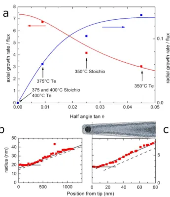
A more regular shape was reported for NWs grown by solid-source MBE [7, 26]. In this case, short NWs feature a pencil-like shape, which is not the focus of the present study. Longer NWs, or NWs involving a final step at low temperature in order to form a shell, exhibit a cone shape and the present model can be used. NWs with the shell grown at different temperatures were observed by SEM (see the inset of Fig. 4b, and Ref [7] for other examples), allowing us to deduce the change of NW radius and length due to the shell-growth step (hence only the cone section is taken into account). Fig. 4 (b) shows the dependance of the axial and radial growth rates, dL/dt and dR/dt, on the tangent of the half angle [7]. These two plots are not independent since tan θ = dR/dL, but it is instructive to plot them separately. A good fit is obtained using Eq. 4 and 5 to calculate dL/dt, with only two adjustable parameters: the value of the flux, which determines the vertical scale, and the diffusion length due to desorption, λdes. The experimental behavior of dL/dt and dR/dt is reproduced using a
Figure 4: InP NWs. (a) MOMBE growth: symbols show the ”migration length” measured in Ref. [24]; the line shows l0 calculated according to Eq. 6, with
λdes=1000 nm and βτ /λdes=0.05; (b) solid-source MBE growth: symbols show
the axial and radial growth rates measured on the cone section of core-shell NWs, as a function of tapering (dR/dL = tan θ); solid lines are the fit (see text) for λdes=1000 nm, dotted lines for λdes=500 nm, dashed lines for λdes=2000 nm;
the inset shows a SEM image (tilt 45◦, scale bar 1 µm) of an InP core-shell NW
Figure 5: ZnTe NWs. (a) axial and radial growth rates, as a function of tapering (tangent of the half angle), and fit (see text). (b) Radius as a function of the distance to the tip, measured on Fig. 1b of Ref. [39]. (c) TEM image and plot, at the same horizontal scale, of the radius as a function of the distance to the tip, sample grown at 320◦C under stoichiometric flux.
constant value λdes=1000 nm, with an increase of the sticking when decreasing
the temperature (not shown), starting from a value which coincides with that of Fig. 4 (a) to within a factor 2. The evolution of the tapering angle is induced by the change of the axial growth rate, with a change of radial growth which is very small and limited to the high temperature range. Increasing or decreasing the value of λdes rapidly modifies the radial growth rate at high temperature,
while the low temperature range is practically unchanged (the radial growth is at saturation). Figure 4 (b) also reveals the almost negligible contribution from the direct flux. This is a consequence of the large value of λdes, for a part, but
also of the geometrical configuration: the flux from the cell makes a large angle, α ∼ 45◦, with the NW axis, and the droplet is quasi-flat [7]. In these conditions
[37], F κ ≃ F cos α = F/√2, and F sin α = F/√2. In Fig. 4 (b), the curves calculated with κ = 0 and κ 6= 0 are undistinguishable.
Turning now to ZnTe, the detailed study of the axial growth rate [28, 36] allowed us to estimate the effective diffusion length λef f. When measured at
different temperatures on the same, single NW [36], λef f is characterized by
a monotonous increase with temperature, but also a minimum value at low temperature which we attribute to the direct flux. In a previous study [28], we used the radial growth in order to determine the nucleation delay and disentangle the axial growth of the NW, for NWs grown under stoichiometric ZnTe flux and with an excess of Te. We also confirmed the strong contribution from the flux to the nanoparticle, with a quasi-spherical profile and a contact area much smaller than the NW section: we estimate κ ≃ 2.5, while sin α = 0.43. In addition, we may expect a significant desorption of the adatoms, as observed in the growth of thick layers [33]. It is thus mandatory to take into account the direct flux. Figure 5 (a) uses the axial growth rate, taken from Ref [28], and the angle taken from the present Fig. 1: it shows that the angle is increased (by decreasing the temperature or adding a Te flux) by a combination of the increase of the radial growth and the decrease of the axial growth. A good fit is obtained by keeping λdes constant at 90 nm: this implies a change of the sticking efficiency (i.e., of
pinc/phop). The role of temperature is further confirmed by the fact that NWs
grown at higher temperature (at 375◦C or 400◦C under stoichiometric ZnTe,
at 400◦C under Te excess) exhibit no radial growth, see Fig. 1, as expected for
conditions below the threshold discussed in Section 4.
A cylinder-shaped tip section is visible in Fig 1 (b) of Ref [39]: the NW was grown directly on the GaAs substrate, the growth mode is VLS and the radius at tip is quite large (R=20 nm). An analysis of the image, Fig. 5 (b), shows that the tapered section starts approximately 230 nm below the tip, in agreement with the present model for the measured half-angle value, tan θ ≈ 0.022. The tip section is expected to be much smaller on NWs with a smaller tip radius (as we obtain on a ZnTe buffer layer) and a stronger tapering. In this case, SEM images are not sufficient as TEM reveals the presence of a 2 to 3 nm thick amorphous layer, which masks the crystalline core (see Fig. 5 (c)). When the core can be identified in spite of the high sensitivity of these thin NWs to the electron beam, a tip section can be observed (Fig. 5 (c)) with a length in good agreement with the value calculated for the measured values of the radius and cone angle.
The influence of the direct flux to the nanoparticle is quite sizable: in the absence of this direct flux, the cylinder section would be longer, see the dashed line in Fig. 5 (b) and (c): in this case (κ = 0 in Eq.4), the axial growth rate is fully ensured by the sidewall flux through the tip terrace. For a given value of dL/dt, adding a contribution from the direct flux to the nanoparticle thus reduces l0. Actually the presence of a direct flux sets an upper limit to the
tapering angle which can be reached by increasing the sticking at steps. At diverging λβτ
des, and for
ls
λdes ≪ 1, Eq. 2 is simplified into
dR
dt = Fα, which is
obviously the upper limit for the radial growth rate; with a lower limit dLdt = κ F for the axial growth rate, an upper limit to the tapering angle is obtained at tan θ = sin απ κ.
Our model assumes that nucleation takes place at the base of the NW, or at least over the bottom section. It appears to be the case for the ZnTe NWs grown
at low temperature, which offer a cone shape over their whole length. When a core-shell NW, made of ZnTe or InP, is realized by starting with a NW grown at high temperature, and finalizing the structure with a second growth step at low temperature, the steps are nucleated on the sidewalls of the initial NW. An interesting case is that of InP NWs grown in the high temperature range [7, 26]: they grow initially with a pencil-like shape, with a rather low radial growth rate. Then, the radial rate increases and they acquire a cone shape. We tentatively ascribe the initial pencil-like shape to a lack of nucleation of steps at the base of the NW, perhaps related to the adatom flux from the sidewalls to the substrate, and not from the substrate to the NW [40]. It is only when the sidewalls are long enough that steps nucleated over the whole length [9, 20, 21] allow the formation of the cone section. The present analysis also suggests that the difference between the InP NWs grown by MBE [7, 26] and those grown by MOMBE [24, 25] are related to a different nucleation of steps, rather than to a different sticking of the adatoms to existing steps: an efficient nucleation in the case of MOMBE allows the formation of the cone-shaped NWs with a long tip terrace, while in MBE pencil-shaped NWs are obtained until the length (or a change of temperature) allows nucleation to take place.
6
Conclusion
A stable configuration is identified for the growth of a NW with nucleation of steps at the base, by equating the velocity of the steps on the sidewalls, and the NW growth rate. The quantities governing the shape are R/a⊥ (radius at
tip in sidewall monolayer units), the desorption-limited diffusion length λdes,
and a combination of parameters βτ /λdes describing the overall efficiency of
sticking at steps. In a microscopic approach, the two relevant parameters are the sticking probability / hopping probability ratio, pinc
phop, and the desorption
probability / hopping probability ratio, pdes
phop.
We identify two extreme domains: (1) if the sticking efficiency βτ /λdes,
although non-zero, is below a threshold ∼ a⊥/R, the sidewall steps remain in
the vicinity of the NW basis, and the axial growth is determined by λdes; this
is the domain of cylinder-shaped NWs, and the conditions to choose in order to insert a quantum dot without the formation of parasitic dots on the sidewalls [26, 27, 41] (2) for a sticking efficiency above this threshold, two segments coexist along the NW, an array of equidistant steps (which govern the radial growth and the cone angle) and a longer tip terrace (which governs the axial growth rate). The NW shape then resembles that calculated for a specific case and described in Fig. 3 (d) of Ref. [23]. At very strong sticking, all parameters are determined by the sticking probability / hopping probability ratio. At moderate sticking, the two probability ratios contribute; when approaching the threshold βτ /λdes ∼ a⊥/R from above, the length of the tip terrace diverges while the
effective diffusion to the nanoparticle (or droplet) is limited by desorption. When applied to InP and ZnTe, the model points to a difference by an order of magnitude of the diffusion length of adatoms limited by desorption. This
difference induces a different behavior of the axial and radial growth rates when adjusting the tapering angle.
Finally, from a practical point of view, the design of a waveguiding shell should take into account the presence of the tip terrace, since its length is of the same order as the wavelength for relevant values of the tapering angle (typically 2◦). In the opposite limit, an upper bound is found for the tapering angle in
the presence of a direct flux to the nanoparticle or droplet.
Acknowledgements
The work at INL was done under the supervision of N. Chauvin, M. Gendry and P. Regreny. The Grenoble teams acknowledge funding by the French Na-tional Research Agency (project Magwires 11-BS10-013, COSMOS ANR-12-JS10-0002, and ESPADON ANR-15-CE24-0029).
A
Details of calculation
A.1
Establishing the equations
We start from the well-known general solution of the BCF model. The adatom density n on a wide terrace with an impinging flux Fα and a time to desorb
τ is n(x) = Fατ ; on a terrace limited by two steps, n(x) is usually looked
for by subtracting a combination of two hyperbolic functions, cosh(x/λdes) and
sinh(x/λdes), with prefactors determined by boundary conditions [31, 33, 34, 35].
Frequently assumed boundary conditions [31] are either perfect sticking at the steps, or perfect sticking at one step and total reflectivity at the other step (the so-called Ehrlich-Schw¨obel effect). In the first case, n = neq at both
steps and we have only the cosh function with its extremum centered on the terrace; in the second case, n = neq at one step and dndx = 0 at the other step,
and again there is only the cosh function, but centered on the reflecting step. Here we assume a perfect trap at the nanoparticle/droplet, and partial sticking at the steps [32]: the regular terrace in the cone is symmetric, but the tip terrace is asymmetric, with different boundary conditions at both ends. The usual method for an asymmetric terrace is to add a sinh function [35], so that the adatom density is characterized by the length of the terrace and the two prefactors of the hyperbolic functions. However, any combination of the two hyperbolic functions can be written as a single, shifted hyperbolic function: if a2> b2, a cosh(x)+b sinh(x) =√a2− b2cosh(x+x
0), with tanh(x0) =ab, and if
a2< b2,√b2− a2sinh(x + x
0) with tanh(x0) =ab. This allows us to look for the
solution with a single hyperbolic function (here a cosh), with three parameters, the prefactor, and the distance of the extremum to each end of the terrace.
The adatom current on the terrace is given by −D dn
dx. The incorporation
into the nanoparticle/droplet must match this current. For incomplete sticking, the incorporation rate at a step is described [35] by a current equal to β (n−neq).
To sum up, the boundary conditions are: • at the NW tip, (n − neq) = 0,
• on each side of each step, β (n − neq) = −D dndx.
We look for n(x) under the unique form (with a single cosh function),
n(x) = Fατ − A(Fατ − neq)
cosh(x/λdes)
cosh(ls/λdes)
. (7)
• The terrace limited by two steps without Ehrlich-Schw¨obel effect is a sym-metrical system, hence we write Eq. 7 with the origin at the terrace center. A is determined by inserting this expression into the boundary condition at step stated above: the result is
A = βτ λdes βτ λdes + tanh( ls λdes) . (8)
This leads to Eq. 1. There is a current of adatoms −D dn
dx on each side of
the step and the step velocity follows, Eq. 2.
• For the tip terrace, using the same expression Eq. 7 with the origin un-known, the boundary condition at the step, and the condition that this leading step has the same velocity as the other steps, determines the posi-tion of the origin at lsfrom the leading step, and the value of the prefactor
A (the same value as above, Eq. 8). The last parameter is the distance between the tip and the origin, l0. The value of l0is obtained by inserting
the expression for n(x) into the boundary condition at tip, and the result is Eq. 3, which can be rewritten:
cosh( l0 λdes) = cosh( ls λdes) βτ λdes+ tanh( ls λdes) βτ λdes (9)
The contribution to the NW growth rate, Eq. 4, follows from the adatom current −D dndx.
A.2
Using the equations
The stability of the NW shape implies the equality between the NW growth rate dLdt and the step velocity Vstep, with
dL
dt = (Fα− Vsub)
2λdestanh(λl0
des)
R + F κ (10)
Vstep = (Fα− Vsub)2λdes
a⊥
βτ tanh( ls
λdes)
βτ + λdestanh(λldess )
(11) = (Fα− Vsub) 2λdes a⊥ sinh(ls/λdes) cosh(l0/λdes) (12)
The first equation is Eq. 4, the second one is Eq. 2, and the third one is Eq. 2 modified using Eq. 3.
Eq. 10 and Eq. 12 contains the experimental data obtained on TEM images (R, ls, l0) and a single material parameter λdes. The stability condition dLdt =
Vstep, written with Eq. 10 and Eq. 12, reads
sin α π 2λdes R [tanh( l0 λdes) − R a⊥ sinh( ls λdes ) 1 cosh( l0 λdes) ] +κ = 0. (13) This is Eq. 5. A second order equation for tanh( l0
λdes) is obtained by using
the relation between cosh( l0
λdes) and tanh(
l0
λdes). This equation can be used to
derive λdesfrom experimental data; it can be used also to study the relationship
between the tip terrace length and the cone angle, for a given value of λdes, as
done in section 5.
We can also calculate ls and l0 as a function of the material parameters
λdes and βτ . This is particularly simple if κ = 0. Then the stability condition
using Eq. 9 and Eq. 11 is simply sinh(l0/λdes) = aR⊥ sinh(ls/λdes); combining
that with cosh(l0/λdes) from Eq. 9, we eliminate l0 and obtain tanh(ls/λdes),
see the first line in Eq. 6. Then, tanh(l0/λdes) follows, second line of (Eq. 6).
These results are used in Section 4. The calculation with κ 6= 0 gives also analytical results at the expense of a second order equation.
References
[1] Claudon J, Bleuse J, Malik N S, Bazin M, Jaffrennou P, Gregersen N, Sauvan C, Lalanne P and G´erard J.-M. 2010 Nat. Photonics 4 174
[2] Reimer M E, Bulgarini G, Akopian N, Hocevar M, Bavinck M B, Verheijen M A, Bakkers E P A M, Kouwenhoven L P and Zwiller V 2012 Nature Com 31
[3] Dalacu D, Mnaymneh K, Lapointe J, Wu X, Poole P J, Bulgarini G, Zwiller V and Reime M E 2012 Nano Lett. 12 5919
[4] Haffouz S, Zeuner K D, Dalacu D, Poole P J, Lapointe J, Poitras D, Mnaym-neh K, Wu X, Couillard M, Korkusinski M, Sch¨oll E, J¨ons K D, Zwiller V and Williams R L 2018 Nano Lett. 18 3047
[5] Zadeh I E, Elshaari A W, J¨ons K D, Fognini A, Dalacu D, Poole P J, Reimer M E and Zwiller V 2016 Nano. Lett. 16 2289
[6] Mnaymneh K, Dalacu D, McKee J, Lapointe J, Haffouz S, Weber J F, North-east D B, Poole P J, Aers G C, Williams 2019 R L Adv. Quantum Tech 1900021
[7] Jaffal A, Redjem W, Regreny P, Nguyen H-S, Cueff S, Letartre X, Patriarche G, Rousseau E, Cassabois G, Gendry M and Chauvin N 2019 Nanoscale 11 21847
[8] Tchernycheva M, Travers L, Patriarche G, Glas F, Harmand J-C, Cirlin G E and Dubrovskii V G 2007 J. Appl. Phys. 102 094313
[9] Dubrovskii V G, Sibirev N V, Cirlin G E, Tchernycheva M, Harmand J C and Ustinov V M 2008 Phys. Rev. E 77 031606
[10] Dubrovskii V G, Timofeeva M A, Tchernycheva M and Bolshakova A D 2013 Semiconductors 47 50
[11] Dubrovskii V G, Sibirev N V, Suris R A, Cirlin G E and Ustinov V M, Tchernysheva M and Harmand J-C 2006 Semiconductors 40 1075
[12] Hofmann S, Sharma R, Wirth C T, Cervantes-Sodi F, Ducati C, Kasama T, Dunin-Borkowski R E, Drucker J, Bennett P and J Robertson 2008 Nature Materials 7372
[13] Wen C-Y, Tersoff J, Reuter M C, Stach E A and F M Ross 2010 Phys. Rev. Lett. 105195502
[14] Harmand J-C, Patriarche G, Glas F, Panciera F, Florea I, Maurice J-L, Travers L and Ollivier Y 2018 Phys. Rev. Lett. 121 166101
[15] Dongare A M, Neurock M and Zhigilei L V 2009 Phys. Rev. B 80, 184106 [16] Wang H, Zepeda-Ruiz L A, Gilmer G H and Upmanyu M 2013 Nature
Communications 4, 1956
[17] Checco A, Guenoun P and Daillant J 2003 Phys. Rev. Lett. 91, 186101 [18] Weijs J H, Marchand A, Andreotti B, Lohse D and Snoeijer J H 2011 Phys.
Fluids 23, 022001
[19] Schmidt V., Senz S and G¨osele U 2005 Appl. Phys. A 80, 445
[20] Chen X L, Lan Y C, Li J Y, Cao Y G and He M 2001 J. Crystal Growth 222586
[21] Plante M C and LaPierre R R 2009 J. Appl. Phys. 105 114304 [22] Filimonov S N and Hervieu Y Yu 2015 J. Cryst. Growth 427 60
[23] Filimonov S N and Hervieu Y Yu 2016 Russian Physics Journal 59 1206 [24] Greenberg Y, Kelrich A, Calahorra Y, Cohen S and Ritter D 2014 J. Crystal
Growth 389103
[25] Kelrich A, Dubrovskii V G, Calahorra Y, Cohen S and Ritter D 2015 Nan-otechnology 26085303
[26] Harmand J-C, Jabeen F, Liu L, Patriarche G, Gauthron K, Senellart P, Elvira D and Beveratos A 2013 J. Crystal Growth 378 519
[27] Rueda-Fonseca P, Bellet-Amalric E, Vigliaturo R, Den Hertog M, Genuist Y, Andr´e R, Robin E, Artioli A, Stepanov P, Ferrand D, Kheng K, Tatarenko S and Cibert J 2014 Nano Lett. 14 1877
[28] Rueda-Fonseca P, Orr`u M, Bellet-Amalric E, Robin E, den Hertog M, Genuist Y, Andr´e R, Tatarenko S and Cibert J 2016 J. Appl. Phys. 119 164303
[29] Chen C, Plante M C, Fradin C and LaPierre R R 2006 J. Materials Research 212801
[30] Burton W K, Cabrera N and Frank F 1951 Phil. Trans. Roy. Soc. 243 299. [31] Pimpinelli A and Villain J 1998 Physics of Crystal Growth (Cambridge
University Press, Cambridge)
[32] Hata M, Isu T, Watanabe A, Kajikawa Y and Katayama Y 1991 J. Cryst. Growth 114203
[33] Pimpinelli A and Peyla P 1998 J. Crystal Growth 183 311
[34] Peyla P, Pimpinelli A, Cibert J and Tatarenko S 1998 J. Crystal Growth 18475
[35] Filimonov S N and Hervieu Y Yu 2014 e-J. Surf. Sci. Nanotech. 12 68 [36] Orr`u M , Robin E, Den Hertog M, Moratis K, Genuist Y, Andr´e R, Ferrand
D, Cibert J and Bellet-Amalric E 2018 Phys. Rev. Materials 2 043404 [37] Glas F 2010 Phys. Statu Sol B 247 254
[38] Dubrovskii V G, Timofeeva M A, Kelrich A, Ritter D 2015 J. Cryst. Growth 41325
[39] Wojnar P, Janik E, Baczewski L T, Kret S, Dynowska E, Wojciechowski T, Suffczy´nski J, Papierska J, Kossacki P, Karczewski G, Kossut J and Wo-jtowicz T 2012 Nano Lett. 12 3404
[40] Harmand J-C, Glas F and Patriarche G 2010 Phys. Rev. B 81 235436 [41] Wojnar P, P lachta J, Zaleszczyk W, Kret S, Sanchez A M, Rudniewski R,
Raczkowska K, Szymura M, Karczewski G, Baczewski L T, Pietruczik A, Wojtowicz T and Kossut J 2016 Nanoscale 8 5720