• Aucun résultat trouvé

Low Temperature Solution-Processable 3D-Patterned Charge Recombination Layer for Organic Tandem Solar Cells

N/A
N/A
Protected

Academic year: 2021

Partager "Low Temperature Solution-Processable 3D-Patterned Charge Recombination Layer for Organic Tandem Solar Cells"

Copied!
12
0
0

Texte intégral

(1)

HAL Id: hal-01972501

https://hal.archives-ouvertes.fr/hal-01972501

Submitted on 7 Jan 2019

HAL is a multi-disciplinary open access

archive for the deposit and dissemination of

sci-entific research documents, whether they are

pub-lished or not. The documents may come from

teaching and research institutions in France or

abroad, or from public or private research centers.

L’archive ouverte pluridisciplinaire HAL, est

destinée au dépôt et à la diffusion de documents

scientifiques de niveau recherche, publiés ou non,

émanant des établissements d’enseignement et de

recherche français ou étrangers, des laboratoires

publics ou privés.

Low Temperature Solution-Processable 3D-Patterned

Charge Recombination Layer for Organic Tandem Solar

Cells

Jin Woo Choi, Jong Woo Jin, Denis Tondelier, Yvan Bonnassieux, Bernard

Geffroy

To cite this version:

Jin Woo Choi, Jong Woo Jin, Denis Tondelier, Yvan Bonnassieux, Bernard Geffroy. Low Temperature

Solution-Processable 3D-Patterned Charge Recombination Layer for Organic Tandem Solar Cells.

Materials, MDPI, 2019, �10.3390/ma12010162�. �hal-01972501�

(2)

Received: 7 December 2018; Accepted: 25 December 2018; Published: 7 January 2019  Abstract: We propose a novel method to pattern the charge recombination layer (CRL) with a low-temperature solution-processable ZnO layer (under 150◦C) for organic solar cell applications. Due to the optimal drying process and thermal annealing condition, ZnO sol-gel particles formed a three-Dimensional (3D) structure without using a high temperature or ramping method. The generated 3D nano-ripple pattern showed a height of around 120 nm, and a valley-to-valley distance of about 500 nm. Based on this newly developed ZnO nano-ripple patterning technique, it was possible to pattern the CRL without damaging the underneath layers in tandem structure. The use of nano-ripple patterned ZnO as the part of CRL, led to the concomitant improvement of the power conversion efficiency (PCE) of about 30%, compared with non-patterned CRL device.

Keywords: organic tandem solar cell; 3D nano-ripple pattern; ZnO sol-gel; charge recombination layer; low temperature solution process

1. Introduction

Finding alternatives for the current energy sources (i.e., burning fossil fuels, nuclear materials) has become one of the most important societal challenges for relieving the environmental pollution problem [1]. One of the most promising next-generation energy sources is solar energy, which can be converted to electric power via photovoltaic technology. Currently industrialized photovoltaic panels are based on inorganic materials such as silicon [2–4]. Recently, organic solar cells (OSCs) emerged as an alternative to inorganic photovoltaics devices [5–7]. The merits of OSC technology are: a low-cost solution process, a low temperature process, flexibility, and a tailorable material for further improvement. Recently, the champion single-junction OSC has reached a power conversion efficiency (PCE) of 12.6% [8]. However, it is still necessary for improving PCE and air-stability for large-scale commercialization.

One of the reasons for the low PCE is the narrow light absorption range of organic materials. A tandem solar cell structure, where two or more single-junction cells with complementary absorption spectra are connected in tandem, can be a promising design to overcome the limitations of single cells [9–11]. A tandem structure offers several advantages: (1) a broad absorption spectrum due to the usage of complementary absorbing materials; (2) summation of the open circuit voltage (VOC) of

each sub-cell; (3) a reasonable fill factor (FF) due to higher optical density over a wider fraction of solar spectrum than that of single cell without increasing internal resistance. To maximize these advantages, the tandem device requires the qualified charge recombination layer (CRL) to simultaneously act as the anode for one of two adjacent sub-cells, and as the cathode for the other [12]. The CRL should have

(3)

low electrical resistance, high optical transparency in the visible range, and a low barrier for charge recombination. Furthermore, the layer should be able to protect the lower layers during the remaining solution fabrication process.

In 2007, the CRL made with a metal oxide material was suggested [13]. The advantage of using a metal oxide as a part of CRL is to minimize the absorption at visible wavelengths. The classical structure of CRL is based on 0.5 nm LiF/1 nm Al/3 nm WoO3, used as multilayers. The first all-solution-processable

tandem OSC was reported by Kim et al., where poly(3,4-ethylenedioxythiophene) polystyrene sulfonate (PEDOT:PSS) and TiOXwere used to form CRL [14]. In 2013, the first inverted tandem OSC that broke 10%

efficiency was reported by You et al., with PEDOT:PSS and ZnO being used as CRL [15]. As shown above, new efficient CRLs with a large work function difference between two opposite interfaces have been developed continuously. Therefore, is high VOCof the tandem device without loss-in-sum of the VOC

of the component cells is achieved. However, maximizing the short circuit current of tandem device is still under development, due to the difficulties in the current matching between the component cells. The current of tandem device is limited by the cell that produces the lower current. Therefore, it is important to increase the short circuit current of each component cell by enhancing the charge extraction properties of CRL. However, to our knowledge, there has been no reported research on the tandem device with patterned CRL, even though the 3D pattern could enhance the charge extraction capability of the CRL.

In the single junction solar cell, patterning of the charge-collecting layer (CCL) has been developed widely to maximize the charge extraction ratio [16–21]. However, previously proposed fabrication techniques for growing nano-wires, nano-rods, and nanoporous layers are not compatible with tandem structure fabrication. High thermal annealing conditions or vacuum processes should be avoided for all solution-processable tandem devices, to prevent the degradation of the films underneath. Meanwhile, a solution-processable ZnO nano-ripple pattern was firstly shown in a single sub-device by Yang et al. in 2009, by using a ramping thermal annealing method [22]. By using patterned ZnO CCL, the PCE improved by about 25% compared with device-containing planar CCL. However, the high thermal annealing treatment condition of this technique (275–350◦C) limited the use of this ripple patterning only in single inverted OSCs [22–24].

Herein, we found the optimal process conditions for nano-ripple patterning of the ZnO film in low-temperature conditions. After confirming the characteristics of ZnO in the single sub-cell device, the layer was introduced as a part of CRL in the tandem device. A newly developed low-temperature process technique actualized the patterning on the CRL without damaging the films underneath. As compared to the non-patterned device, the tandem device with ZnO ripple-patterned CRL showed a PCE improvement of about 30%.

2. Experimental Section

As shown in Figure 1, for electron-only devices, ZnO films with different pattern sizes, single-junction OSCs, and tandem OSCs with a ZnO layer were fabricated and analyzed. The detailed fabrication methods are described below.

(4)

Figure 1. Device structures used in this study, with relevant energy levels of the different layers. (a) Electron only device, (b) single solar cell with a nano-ripple pattern, (c) tandem solar cell. ECL (electron collecting layer) and HCL (hole-collecting layer) are the ZnO nano-ripple layer and the PEDOT:PSS:Triton layer respectively.

2.1. Preparation of Solutions

A ZnOX sol-gel solution was prepared by the following method. Zinc acetate dehydrate (ZnO

precursor) at 1.5 M concentration was prepared in 2-methoxyethanol, followed by adding 0.1 mL of ethanolamine. Two types of PEDOT:PSS (Al4083 and PH1000, respectively) with surfactant were used as the hole-collecting layer. A volume of 100 µL of surfactant Triton was mixed with 4 mL of 1:1 volume ratio of AI4083 and PH1000. The ratio of PEDOT:PSS was 1:6 for Al4083, and 1:2.5 for PH1000. PH1000 contains higher amount of PEDOT, and thus has a higher conductivity than AI4083. AI4083 and PH1000 were purchased from Bayer (Leverkusen, Germany). In solar cells, poly(3-hexylthiophene) (P3HT) and poly[[4,8-bis[(2-ethylhexyl)oxy]benzo[1,2-b:4,5-b']dithiophene-2,6-diyl][3-fluoro-2-[(2-ethylhexyl)carbonyl]thieno[3,4-b]thiophenediyl]] (PTB7) were used as the donor materials, while 1′,1′′,4′,4′′-tetrahydro-di[1,4]methanonaphthaleno[1,2:2′,3′,56,60:2′′,3′′][5,6]fullerene-C60 (ICBA), 6,6-phenyl C61-butyric acid methyl ester (PCBM), and 6,6-phenyl C71-butyric acid methyl ester (PC70BM) were used as acceptor materials. P3HT, PTB7, and fullerene derivatives were

purchased from Ossila (Sheffield, UK). For a single solar cell (Figure 1b), a blend of P3HT and PCBM (1:1 weight ratio) was used as the active layer by dissolving 40 mg of P3HT:PCBM in 1 mL 1,2-dichlorobenzene (DCB, Sigma Aldrich, St. Louis, MO, USA). For the tandem solar cell (Figure 1c), the first cell (bottom cell, Figure 1c) was based on a blend of P3HT and ICBA, and the second sub-cell (top sub-cell, Figure 1c) was a blend of PTB7 and PC70BM. The P3HT:ICBA blend solution was

prepared by dissolving 40 mg of P3HT:ICBA (1:1 weight ratio) in 1 mL of DCB. For second sub-cell active layer, the solution was prepared by dissolving 1:1.5 weight ratio of PTB7:PC70BM in DCB with

a total concentration of 25 mg/mL. All prepared solutions were stirred for 12 h in a N2 glove box.

2.2. Electron-Only Device

An aluminum layer of 100 nm thickness was deposited onto glass substrates by thermal evaporation. The deposition rate of Al was 0.25 Å/s under 5 × 10⁻⁷ Torr process pressure. Prepared

ZnO sol-gel solution was spin-coated on the Al deposited glass through a 0.45 µm pore polyvinylidene fluoride (PVDF) filter at 1000 rpm for 60 s. The obtained films were dried in ambient air over 5, 10, 30, 60, and 180 min, respectively, and then thermally annealed over 10 min at 125, 150, 175, and 200 °C, respectively. The final thickness of the films was 400 nm. For top electrode, 100 nm thick aluminum layer was thermally evaporated through a shadow mask, defining a device area of 0.28 cm2. The deposition condition of Al was same as the bottom electrode. ZnO film obtained by

ramping method, as described by Yang group, was also prepared for comparison [21]. The current-Figure 1. Device structures used in this study, with relevant energy levels of the different layers. (a) Electron only device, (b) single solar cell with a nano-ripple pattern, (c) tandem solar cell. ECL (electron collecting layer) and HCL (hole-collecting layer) are the ZnO nano-ripple layer and the PEDOT:PSS:Triton layer respectively.

2.1. Preparation of Solutions

A ZnOXsol-gel solution was prepared by the following method. Zinc acetate dehydrate (ZnO

precursor) at 1.5 M concentration was prepared in 2-methoxyethanol, followed by adding 0.1 mL of ethanolamine. Two types of PEDOT:PSS (Al4083 and PH1000, respectively) with surfactant were used as the hole-collecting layer. A volume of 100 µL of surfactant Triton was mixed with 4 mL of 1:1 volume ratio of AI4083 and PH1000. The ratio of PEDOT:PSS was 1:6 for Al4083, and 1:2.5 for PH1000. PH1000 contains higher amount of PEDOT, and thus has a higher conductivity than AI4083. AI4083 and PH1000 were purchased from Bayer (Leverkusen, Germany). In solar cells, poly(3-hexylthiophene) (P3HT) and poly[[4,8-bis[(2-ethylhexyl)oxy]benzo[1,2-b:4,5-b’]dithiophene-2,6-diyl][3-fluoro-2-[(2-ethylhexyl)carbonyl]thieno[3,4-b]thiophenediyl]] (PTB7) were used as the donor materials, while 10,1”,40,4”-tetrahydro-di[1,4]methanonaphthaleno[1,2:20,30,56,60:2”,3”][5,6]fullerene-C60 (ICBA), 6,6-phenyl C61-butyric acid methyl ester (PCBM), and 6,6-phenyl C71-butyric acid methyl ester (PC70BM) were used as acceptor materials. P3HT, PTB7, and fullerene derivatives were purchased

from Ossila (Sheffield, UK). For a single solar cell (Figure1b), a blend of P3HT and PCBM (1:1 weight ratio) was used as the active layer by dissolving 40 mg of P3HT:PCBM in 1 mL 1,2-dichlorobenzene (DCB, Sigma Aldrich, St. Louis, MO, USA). For the tandem solar cell (Figure1c), the first sub-cell (bottom cell, Figure 1c) was based on a blend of P3HT and ICBA, and the second sub-cell (top cell, Figure1c) was a blend of PTB7 and PC70BM. The P3HT:ICBA blend solution was prepared by

dissolving 40 mg of P3HT:ICBA (1:1 weight ratio) in 1 mL of DCB. For second sub-cell active layer, the solution was prepared by dissolving 1:1.5 weight ratio of PTB7:PC70BM in DCB with a total

concentration of 25 mg/mL. All prepared solutions were stirred for 12 h in a N2glove box.

2.2. Electron-Only Device

An aluminum layer of 100 nm thickness was deposited onto glass substrates by thermal evaporation. The deposition rate of Al was 0.25 Å/s under 5×10⁻⁷Torr process pressure. Prepared ZnO sol-gel solution was spin-coated on the Al deposited glass through a 0.45 µm pore polyvinylidene fluoride (PVDF) filter at 1000 rpm for 60 s. The obtained films were dried in ambient air over 5, 10, 30, 60, and 180 min, respectively, and then thermally annealed over 10 min at 125, 150, 175, and 200◦C, respectively. The final thickness of the films was 400 nm. For top electrode, 100 nm thick aluminum layer was thermally evaporated through a shadow mask, defining a device area of 0.28 cm2. The deposition condition of Al was same as the bottom electrode. ZnO film obtained by ramping

(5)

method, as described by Yang group, was also prepared for comparison [21]. The current-voltage (I-V) characteristics of the ZnO electron-only device were measured by a Keithley 4200 (Tektronix, Beaverton, OR, USA). Atomic force microscopy (AFM) was used for the imaging of the 3D pattern of the fabricated samples.

2.3. Organic Solar Cell Fabrication and Characterization

OSCs were fabricated on ITO substrates (sheet resistance 20Ω/square) purchased from Xinyan Technologies (Kowloon, Hong Kong). Pre-patterned ITO coated glass substrates were cleaned in an ultrasonic cleaner with deionized water and isopropyl alcohol (IPA) for 20 min each.

For single solar cell (Figure1b), prepared ZnO sol-gel solution was deposited onto the ITO layer by spin coating (3000 rpm for 60 s) through a 0.45 µm pore PVDF filter in a N2glove box. The substrates

were directly transferred outside the glove box and dried in ambient air during different times (0, 5, 10, 30, 60, and 180 min, respectively) and then thermally annealed at 125◦C over 10 min, in order to form nano-ripple structures. The final thickness of the fabricated film was 200 nm. The samples were then transferred into N2glove box to deposit the following layers. A P3HT:PCBM solution

was filtered through a 0.45 µm pore polytetrafluoroethylene (PTFE) filter, and spin-coated in two steps (500 rpm for 30 s, and then 1000 rpm for 45 s). The films were thermally annealed at 145◦C for 10 min. The thickness of this layer was approximately 100 nm after annealing. Then, PEDOT:PSS:Triton solution was deposited at 1000 rpm for 60 s. The thickness of this layer was 120 nm after annealing at 120◦C for 2 min.

For tandem cells (Figure1c), the ZnO nano-ripple layer (ECL), the first sub-cell active layer, and PEDOT:PSS:Triton layer (HCL) were fabricated in the same way as reported above. PTB7:PC70BM

was used as active layer in the second sub-cell. The PTB7:PC70BM solution was filtered through

a 0.45 µm pore PTFE filter, and spin-coated at 700 rpm for 60 s. The layer was annealed in DCB solvent vapor for 5 min. The thickness of this layer was approximately 80 nm. Finally, a gold electrode (anode) was thermally evaporated through a shadow mask, defining a 0.28 cm2active surface area. The deposition rate of Au was 0.5 Å/s under 5×10⁻⁶Torr process pressure.

The current density-voltage (J-V) characteristics of the OSCs were measured in a N2glove box

using a source meter (Keithley 2635, Tektronix, Beaverton, OR, USA) in the dark and under illumination. An Air-Mass 1.5 (AM 1.5) solar simulator with 100 mW cm−2was used as the light source.

3. Results and Discussion

3.1. ZnO Electron Collection Layer

To find the optimal annealing temperature for ZnO films, electron-only devices were fabricated to evaluate the conductivity of ZnO films under different thermal annealing conditions [25]. Figure2

shows the I-V characteristics of Al/ZnO/Al electron-only device, with 400 nm thick ZnO. Table1

summarizes the conductivity extracted from the I-V characteristics. The film made with the ramping fabrication method shows the highest conductivity among all films, but the difference is weak, and the conductivity values are in the same order of magnitude. A factor of 3 was observed between the lowest temperature annealing temperature (125◦C) and the ramping method (350◦C). It is obvious that the conductance of the ZnO thin film becomes higher when the film was annealed at higher temperature. Generally, a high annealing temperature provides a better crystallinity of the films, which directly impacts on the conductivity [26,27]. The reaction phenomena of ZnO sol-gel is reported in a previous report [28]. The ZnO precursor (zinc acetate dehydrate) film is highly resistive, because of the acetate functional group. Therefore, an annealing process is required to induce the reaction between the ZnO precursor with 2-methoxyethanol and the oxidation of a ZnO precursor in air. However, thermal annealing treatments of higher than 200◦C were not considered in this study, since the high annealing temperature of CRL could cause damage on the underlying layers in a tandem structure. It is then shown that the annealing temperature could be lowered to 125◦C.

(6)

Figure 2. I-V characteristics of an Al (100 nm)/ZnO (400 nm)/Al (100 nm) electron-only diode device with a ZnO thickness of 400 nm.

Table 1. Conductivity value of the ZnO films under different annealing temperatures.

Temperature 125 °C 150 °C 175 °C 200 °C Ramping 350 °C

Conductivity (S/m) 2.5 × 10⁻³ 3.5 × 10⁻³ 4.4 × 10⁻³ 6.7 × 10⁻³ 7.3 × 10⁻³

3.2. ZnO Ripple Pattern

Based on the idea that ZnO ripple pattern growth mechanism is analogous to the coffee ring effect [27,29,30] and the solvent annealing technique [31], ZnO films were dried in the air at ambient temperature over various time periods (from 0 to 3 h) before annealing. After that, they were placed on a hot plate for thermal treatment over 10 minutes at 125, 150, 175, and 200 °C, respectively. Peak-to-valley roughness values (RPtoV) of patterned ZnO films, measured by AFM, are summarized in

Table 2. The highest RPtoV values for each annealing temperature were as follows: 110 nm at 125 °C,

122 nm at 150 °C, and 113 nm at 175 °C, achieved when the drying time was 60, 10, and 5 min, respectively. Devices with a short drying time require a high annealing temperature for the optimum pattern, i.e., the highest RPtoV value. This result is reasonable, because short dried samples has more

remaining solvent [32]. The sample will need a higher temperature to remove the remaining solvent, and consequently, to form the pattern. During the drying process, the films will partially dry, and small ZnO particles (cross-linked ZnO precursors) begin to form inside the film. These particles will travel, following the convection current of the solvent during thermal annealing of the film. Changing the drying time affects the initial size of seed crystal particles and the amount of the remaining solvent, which modifies the convection flow and the coffee ring effect [29,32]. The device with the highest RPtoV was achieved at 150 °C after 10 min of drying time. The RPtoV values were abruptly

decreased with a long drying time (3 h) and a high annealing temperature (200 °C). The lack of remaining solvent due to the long drying process or fast evaporation at high temperature hinders the convection flow, and consequently, the rearrangement of ZnO precursor to form a 3D pattern.

Table 2. RPtoV value of ZnO films with different drying times and annealing temperatures (units in nm).

Drying Time Annealing Temperature

125 °C 150 °C 175 °C 200 °C

0 min 78 109 93 21

5 min 84 111 113 22

Figure 2.I-V characteristics of an Al (100 nm)/ZnO (400 nm)/Al (100 nm) electron-only diode device with a ZnO thickness of 400 nm.

Table 1.Conductivity value of the ZnO films under different annealing temperatures. Temperature 125C 150C 175C 200C Ramping 350C Conductivity (S/m) 2.5×10⁻³ 3.5×10⁻³ 4.4×10⁻³ 6.7×10⁻³ 7.3×10⁻³

3.2. ZnO Ripple Pattern

Based on the idea that ZnO ripple pattern growth mechanism is analogous to the coffee ring effect [27,29,30] and the solvent annealing technique [31], ZnO films were dried in the air at ambient temperature over various time periods (from 0 to 3 h) before annealing. After that, they were placed on a hot plate for thermal treatment over 10 min at 125, 150, 175, and 200◦C, respectively. Peak-to-valley roughness values (RPtoV) of patterned ZnO films, measured by AFM, are summarized in Table2.

The highest RPtoVvalues for each annealing temperature were as follows: 110 nm at 125◦C, 122 nm at

150◦C, and 113 nm at 175◦C, achieved when the drying time was 60, 10, and 5 min, respectively. Devices with a short drying time require a high annealing temperature for the optimum pattern, i.e., the highest RPtoVvalue. This result is reasonable, because short dried samples has more remaining solvent [32].

The sample will need a higher temperature to remove the remaining solvent, and consequently, to form the pattern. During the drying process, the films will partially dry, and small ZnO particles (cross-linked ZnO precursors) begin to form inside the film. These particles will travel, following the convection current of the solvent during thermal annealing of the film. Changing the drying time affects the initial size of seed crystal particles and the amount of the remaining solvent, which modifies the convection flow and the coffee ring effect [29,32]. The device with the highest RPtoVwas achieved at 150◦C after

10 min of drying time. The RPtoVvalues were abruptly decreased with a long drying time (3 h) and

a high annealing temperature (200◦C). The lack of remaining solvent due to the long drying process or fast evaporation at high temperature hinders the convection flow, and consequently, the rearrangement of ZnO precursor to form a 3D pattern.

The AFM images of the best nano-ripple pattern fabricated by a low temperature process, and the pattern obtained by ramping method, are shown in Figure3. Pattern sizes with the novel low temperature method (Figure3a) showed similar RPtoVvalue to that achieved by the ramping method (Figure3b).

(7)

followed by annealing temperature of 150◦C during 10 min. Finally, we succeed on the fabrication of 3D nano-patterned ZnO film, without using a high temperature, by introducing the drying step in the process.

Table 2.RPtoVvalue of ZnO films with different drying times and annealing temperatures (units in nm).

Drying Time Annealing Temperature 125C 150C 175C 200C 0 min 78 109 93 21 5 min 84 111 113 22 10 min 96 122 110 19 30 min 102 106 99 21 60 min 110 98 93 22 3 h 43 87 83 21

Materials 2018, 11, x FOR PEER REVIEW 6 of 11

10 min 96 122 110 19

30 min 102 106 99 21

60 min 110 98 93 22

3 h 43 87 83 21

The AFM images of the best nano-ripple pattern fabricated by a low temperature process, and the pattern obtained by ramping method, are shown in Figure 3. Pattern sizes with the novel low temperature method (Figure 3a) showed similar RPtoV value to that achieved by the ramping method

(Figure 3b). RPtoV value of ZnO film fabricated by ramping method was 135 and 120 nm for drying

time of 10 min followed by annealing temperature of 150 °C during 10 min. Finally, we succeed on the fabrication of 3D nano-patterned ZnO film, without using a high temperature, by introducing the drying step in the process.

Figure 3. Atomic force microscopy (AFM) images of the ZnO nano-ripple, (a) the low temperature processed (10 minutes of drying time and annealing temperature of 150 °C) and (b) the ramping method.

3.3. Single Junction Solar Cell with A 3D Nano-Patterned ZnO Layer

The inverted devices have a structure of ITO/ZnO/P3HT:PCBM (200 nm)/PEDOT:PSS (100nm)/Al (100 nm) with a different ripple size of the ZnO layer. Figure 4 shows J-V characteristics of the inverted devices made with P3HT:PCBM under 100 mW/cm2 illumination. The performance

characteristics of the OSCs are summarized in Table 3. Devices A to D were fabricated in a low-temperature process, with an annealing low-temperature of 150 °C for 10 min and different drying times. The drying time was 3000, 300, 60, and 10 min for devices A, B, C, and D, respectively. As previously shown in Table 2, the drying time modifies the pattern size (RPtoV) for a fixed temperature. Only

drying time was controlled to change the 3D pattern size (RPtoV), in order to exclude the effects of the

annealing temperature on the film properties, such as conductivity. The J-V curve that is labeled device E shows the characteristics of OSC, with the ZnO layer being made by the ramping method. Even though the ramping method could give a slightly better conductivity as shown in Table 1, the overall characteristic of device D shows similar characteristic with device E. The short circuit current (JSC) and FF increase as the ZnO pattern size increases, while VOC does not show a significant change.

As a result, the device with 120 nm RPtoV has the best performance, with 3.4% of PCE. The

improvements on the JSC and FF are based on the efficient charge collection properties, by introducing

a patterned ZnO layer. Due to the efficient carrier extraction, the space charge-inducing resistance near ECL will be reduced. When the pattern size of ZnO increases from 80 to 120 nm, an expectable result is a decrease in the series resistance. The series resistances extracted by the slope of the J-V curve at the VOC were 27, 25, 21, and 21 Ω∙cm2 for device A, B, C, and D, respectively.

Figure 3. Atomic force microscopy (AFM) images of the ZnO nano-ripple, (a) the low temperature processed (10 min of drying time and annealing temperature of 150◦C) and (b) the ramping method.

3.3. Single Junction Solar Cell with A 3D Nano-Patterned ZnO Layer

The inverted devices have a structure of ITO/ZnO/P3HT:PCBM (200 nm)/PEDOT:PSS (100 nm)/Al (100 nm) with a different ripple size of the ZnO layer. Figure4shows J-V characteristics of the inverted devices made with P3HT:PCBM under 100 mW/cm2illumination. The performance characteristics of the OSCs are summarized in Table3. Devices A to D were fabricated in a low-temperature process, with an annealing temperature of 150◦C for 10 min and different drying times. The drying time was 3000, 300, 60, and 10 min for devices A, B, C, and D, respectively. As previously shown in Table2, the drying time modifies the pattern size (RPtoV) for a fixed temperature. Only drying time was controlled

to change the 3D pattern size (RPtoV), in order to exclude the effects of the annealing temperature on the

film properties, such as conductivity. The J-V curve that is labeled device E shows the characteristics of OSC, with the ZnO layer being made by the ramping method. Even though the ramping method could give a slightly better conductivity as shown in Table1, the overall characteristic of device D shows similar characteristic with device E. The short circuit current (JSC) and FF increase as the ZnO pattern size increases,

while VOCdoes not show a significant change. As a result, the device with 120 nm RPtoVhas the best

performance, with 3.4% of PCE. The improvements on the JSCand FF are based on the efficient charge

collection properties, by introducing a patterned ZnO layer. Due to the efficient carrier extraction, the space charge-inducing resistance near ECL will be reduced. When the pattern size of ZnO increases from 80 to 120 nm, an expectable result is a decrease in the series resistance. The series resistances extracted by the slope of the J-V curve at the VOCwere 27, 25, 21, and 21Ω·cm2for device A, B, C, and D, respectively.

(8)

Figure 4. Current–voltage characteristics of the solar cells with different nano-patterned sizes of the ZnO electron-collecting layer (ECL). (ramp.) stands for the ramping method.

Table 3. The summary of the key parameters of the single junction organic solar cells (OSCs), with different nano-ripple pattern sizes. Devices A to D were fabricated by the low-temperature method, while device E was fabricated by the ramping method.

Device X Pattern Size (nm) Voc (V) JSC (mA/cm2) FF (%) PCE (%) Rs (Ω∙cm2) A 0 0.54 −9.0 56 2.7 27 B 80 0.54 −9.3 56 2.8 25 C 100 0.55 −9.9 61 3.3 21 D 120 0.55 −10.3 60 3.4 21 E 135 0.55 −10.3 61 3.4 21

To assess the effect of ZnO layer on the electrical properties of the device more deeply, we examined the charge collection probability (Pcollection) in the cells, according to the method proposed

by Kyaw et al. [33]. A photo-generated current (Jph) is saturated at the high internal voltage (Vint)

region, due to the large enough internal field extracted all generated charges. Therefore, the saturated photocurrent (Jph,saturation) can be written as following equation, while the value is limited only by the

number of absorbed photons:

Jph,saturation = qLGmax (1)

q is the elementary charge, L is the thickness of the active layer, and Gmax is the maximum

photoinduced carrier generation rate per unit volume. However, in a low internal voltage region, the Jph is proportional to the Pcollection in the cells. Therefore, the equation 1 can be written as:

Jph,saturation = qLGmax Pcollection (2)

From Equations (1) and (2), Pcollection can be calculated by normalizing Jph with Jph,saturation.

Figure 5 shows the charge collection probability with respect to internal voltage (Vint) under

illumination of 100 mW/cm2. As shown in Figure 5, the overall charge collection probability of the

inverted devices with ZnO increased, as the pattern size increases. The increment in charge collection probability is more significant at low Vint (high applied voltage). The observed increment of charge

collection probability in the nano-patterned ZnO devices is well-matched with the JSC characteristic

of the OSCs.

Figure 4.Current–voltage characteristics of the solar cells with different nano-patterned sizes of the ZnO electron-collecting layer (ECL). (ramp.) stands for the ramping method.

Table 3.The summary of the key parameters of the single junction organic solar cells (OSCs), with different nano-ripple pattern sizes. Devices A to D were fabricated by the low-temperature method, while device E was fabricated by the ramping method.

Device X Pattern Size (nm) Voc (V) JSC (mA/cm2) FF (%) PCE (%) Rs (Ω·cm2) A 0 0.54 −9.0 56 2.7 27 B 80 0.54 −9.3 56 2.8 25 C 100 0.55 −9.9 61 3.3 21 D 120 0.55 −10.3 60 3.4 21 E 135 0.55 −10.3 61 3.4 21

To assess the effect of ZnO layer on the electrical properties of the device more deeply, we examined the charge collection probability (Pcollection) in the cells, according to the method proposed

by Kyaw et al. [33]. A photo-generated current (Jph) is saturated at the high internal voltage (Vint)

region, due to the large enough internal field extracted all generated charges. Therefore, the saturated photocurrent (Jph,saturation) can be written as following equation, while the value is limited only by the

number of absorbed photons:

Jph,saturation= qLGmax (1)

q is the elementary charge, L is the thickness of the active layer, and Gmaxis the maximum photoinduced

carrier generation rate per unit volume. However, in a low internal voltage region, the Jphis proportional

to the Pcollectionin the cells. Therefore, the equation 1 can be written as:

Jph,saturation= qLGmaxPcollection (2)

From Equations (1) and (2), Pcollectioncan be calculated by normalizing Jphwith Jph,saturation.

Figure5shows the charge collection probability with respect to internal voltage (Vint) under

illumination of 100 mW/cm2. As shown in Figure5, the overall charge collection probability of the inverted devices with ZnO increased, as the pattern size increases. The increment in charge collection probability is more significant at low Vint(high applied voltage). The observed increment of charge

collection probability in the nano-patterned ZnO devices is well-matched with the JSCcharacteristic of

(9)

Materials 2019, 12, 162 8 of 11

Figure 5. Charge collection probability as a function of the internal voltage for cells with different

ZnO nano-pattern size.

3.4. Tandem Solar Cell with Low-Temperature Processed ZnO

Photoactive layers with complementary absorption range were used as sub-cells of the tandem

device. P3HT:ICBA was selected as the active layer for the bottom cell (device F and G). ICBA was

selected as the acceptor, because the P3HT:ICBA active layer forms its optimal morphology in higher

annealing temperature when compared with P3HT:PCBM [34–36]. Therefore, the P3HT:ICBA system

promises a lower thermal degradation for tandem device fabrication, compared with the

P3HT:PCBM system. The PTB7:PC

70

BM active layer is selected for the top cell (device H and I).

Instead of thermal annealing, the solvent annealing method was used for the PTB7:PC

70

BM active

layer, to minimize the thermal effect on the underneath layers in the tandem device process [37]. The

sub-cells have the structure: ITO/ZnO (150 nm)/P3HT:ICBA (100 nm) or PTB7:PC

70

BM (150

nm)/PEDOT:PSS (120 nm)/Au (100 nm). The details of structure and photovoltaic devices

performance are summarized in Table 4. Figure 6 presents the effect of the ZnO ripple pattern on the

performance of each sub-cell. Among the devices F to I, devices with patterned ZnO show better J

SC

and PCE. Likewise in the device with P3HT:PCBM, the increment of charge collection probability in

the nano-patterned ZnO layer is the origin of these improvements. The inverted tandem devices have

a structure of ITO/ZnO (150 nm)/P3HT:ICBA (100 nm)/PEDOT:PSS (120 nm)/ZnO (150

nm)/PTB7:PC

70

BM (150 nm)/PEDOT:PSS/Au (100 nm). The V

OC

values of fabricated tandem devices

are much higher than V

OC

of each sub-cell (Table 4). This means that the sub-cells were series

connected through CRL. V

OC

of P3HT:ICBA device and PTB7:PC

70

BM device is 0.78 and 0.73 V,

respectively. Therefore, ideally expected V

OC

for tandem device is 1.5 V. Comparing this ideal value

with V

OC

of the fabricated tandem devices, there was only slight loss at around 0.1 to 0.2 V. A tandem

device with a 3D nano-patterned ZnO (device K) shows a higher V

OC

, J

SC

, and FF than the device with

pristine ZnO (device J). A better work function matching of CRL with active layers, efficient electron

extraction, and electron-hole balance in the device are the reasons for this improvement [38,39]. A

highly efficient carrier recombination characteristic of the CRL in a patterned ZnO layer reduced

charge accumulation effect. Finally, the best device achieved a V

OC

of 1.38 V, a J

SC

of −7.2 mA/cm

2

, a

FF of 49%, and PCE of 4.8%.

Figure 5.Charge collection probability as a function of the internal voltage for cells with different ZnO nano-pattern size.

3.4. Tandem Solar Cell with Low-Temperature Processed ZnO

Photoactive layers with complementary absorption range were used as sub-cells of the tandem device. P3HT:ICBA was selected as the active layer for the bottom cell (device F and G). ICBA was selected as the acceptor, because the P3HT:ICBA active layer forms its optimal morphology in higher annealing temperature when compared with P3HT:PCBM [34–36]. Therefore, the P3HT:ICBA system promises a lower thermal degradation for tandem device fabrication, compared with the P3HT:PCBM system. The PTB7:PC70BM active layer is selected for the top cell (device H and I). Instead of thermal

annealing, the solvent annealing method was used for the PTB7:PC70BM active layer, to minimize

the thermal effect on the underneath layers in the tandem device process [37]. The sub-cells have the structure: ITO/ZnO (150 nm)/P3HT:ICBA (100 nm) or PTB7:PC70BM (150 nm)/PEDOT:PSS

(120 nm)/Au (100 nm). The details of structure and photovoltaic devices performance are summarized in Table 4. Figure 6 presents the effect of the ZnO ripple pattern on the performance of each sub-cell. Among the devices F to I, devices with patterned ZnO show better JSCand PCE. Likewise

in the device with P3HT:PCBM, the increment of charge collection probability in the nano-patterned ZnO layer is the origin of these improvements. The inverted tandem devices have a structure of ITO/ZnO (150 nm)/P3HT:ICBA (100 nm)/PEDOT:PSS (120 nm)/ZnO (150 nm)/PTB7:PC70BM

(150 nm)/PEDOT:PSS/Au (100 nm). The VOCvalues of fabricated tandem devices are much higher

than VOCof each sub-cell (Table4). This means that the sub-cells were series connected through CRL.

VOCof P3HT:ICBA device and PTB7:PC70BM device is 0.78 and 0.73 V, respectively. Therefore, ideally

expected VOC for tandem device is 1.5 V. Comparing this ideal value with VOC of the fabricated

tandem devices, there was only slight loss at around 0.1 to 0.2 V. A tandem device with a 3D nano-patterned ZnO (device K) shows a higher VOC, JSC, and FF than the device with pristine ZnO

(device J). A better work function matching of CRL with active layers, efficient electron extraction, and electron-hole balance in the device are the reasons for this improvement [38,39]. A highly efficient carrier recombination characteristic of the CRL in a patterned ZnO layer reduced charge accumulation effect. Finally, the best device achieved a VOCof 1.38 V, a JSCof−7.2 mA/cm2, a FF of 49%, and PCE

(10)

Figure 6. The J-V characteristics of the OSC devices with and without a ZnO patterned layer as ECL. Table 4. The summary of the key parameters of the OSCs extracted from the J-V measurements. ECL stands for the electron collecting layer (ZnO layer).

Device Structure ECL (ZnO Layer) VOC (V) Jsc (mA/cm2) FF (%) PCE (%) F

First sub-cell Non-patterned 0.79 −7.6 51 3.1

G Nano-ripple 0.78 −8.8 50 3.5 H Second sub-cell Non-patterned 0.73 −10.2 48 3.6 I Nano-ripple 0.73 −11.9 48 4.2 J

Tandem cell Non-patterned 1.28 −6.5 44 3.7

K Nano-ripple 1.38 −7.2 49 4.8

4. Conclusion

We developed a new method for patterning the ZnO layer by a low temperature (under 150 °C) solution process. A solution-processable ZnO layer shows proper electrical characteristics for OSCs even with a low temperature process. Nano-ripple pattern was fabricated to maximize the interface between the ZnO layer and the photoactive layer. In a single-junction device, PCE was about 30% higher when the ZnO layer was patterned. Finally, developed low-temperature processable nano-patterned ZnO was introduced in the tandem structure. The best tandem device has VOC of 1.38 V

and PCE of 4.8%, showing nearby 30% PCE improvement, compared to the non-patterned injection layer. It is shown that main improvement results from the charge extraction probability improvement, due to the nano-ripple patterned layer.

Author Contributions: J.W.C., Y.B., and B.G. conceived and designed the experiments; J.W.C., J.W.J., and D.T. performed the experiments; J.W.C. and B.G. analyzed the data; J.W.C. and B.G. wrote the paper.

Acknowledgments: J.C. would like to thank ED Polytechnique for the PhD funding. Conflicts of Interest: The authors declare no conflict of interest.

References

1. BP. BP Statistical Review of World Energy; British Petroleum Company: London, UK, 2014; pp. 1–48. 2. El Chaar, L.; Lamont, L.A.; El Zein, N. Review of Photovoltaic Technologies. Renew. Sustain. Energy Rev.

2011, 15, 2165–2175.

3. Becquerel, E. Mémoire sur les effets électriques produits sous l’influence des rayons solaires. C. R. Acad.

Sci. Paris 1839, 9, 561–567.

Figure 6.The J-V characteristics of the OSC devices with and without a ZnO patterned layer as ECL. 4. Conclusions

We developed a new method for patterning the ZnO layer by a low temperature (under 150◦C) solution process. A solution-processable ZnO layer shows proper electrical characteristics for OSCs even with a low temperature process. Nano-ripple pattern was fabricated to maximize the interface between the ZnO layer and the photoactive layer. In a single-junction device, PCE was about 30% higher when the ZnO layer was patterned. Finally, developed low-temperature processable nano-patterned ZnO was introduced in the tandem structure. The best tandem device has VOCof 1.38 V and PCE of 4.8%,

showing nearby 30% PCE improvement, compared to the non-patterned injection layer. It is shown that main improvement results from the charge extraction probability improvement, due to the nano-ripple patterned layer.

Author Contributions:J.W.C., Y.B., and B.G. conceived and designed the experiments; J.W.C., J.W.J., and D.T. performed the experiments; J.W.C. and B.G. analyzed the data; J.W.C. and B.G. wrote the paper.

Acknowledgments:J.C. would like to thank ED Polytechnique for the PhD funding. Conflicts of Interest:The authors declare no conflict of interest.

References

1. BP. BP Statistical Review of World Energy; British Petroleum Company: London, UK, 2014; pp. 1–48.

2. El Chaar, L.; Lamont, L.A.; El Zein, N. Review of Photovoltaic Technologies. Renew. Sustain. Energy Rev. 2011, 15, 2165–2175. [CrossRef]

3. Becquerel, E. Mémoire sur les effets électriques produits sous l’influence des rayons solaires. C. R. Acad. Sci. Paris 1839, 9, 561–567.

(11)

4. Chapin, D.M.; Fuller, C.S.; Pearson, G.L. A New Silicon p-n Junction Photocell for Converting Solar Radiation into Electrical Power. J. Appl. Phys. 1954, 25, 676–677. [CrossRef]

5. Hoppe, H.; Sariciftci, N.S. Organic solar cells: An overview. J. Mater. Res. 2011, 19, 1924–1945. [CrossRef] 6. Wohrle, D.; Meissner, D. Organic Solar Cells. Adv. Mater. 1991, 3, 129–138. [CrossRef]

7. Gregg, B.A. Excitonic solar cells. J. Phys. Chem. B 2003, 107, 4688–4698. [CrossRef]

8. Available online: https://www.nrel.gov/pv/assets/pdfs/pv-efficiencies-07-17-2018.pdf(accessed on 7 December 2018).

9. Cheyns, D.; Rand, B.P.; Heremans, P. Organic tandem solar cells with complementary absorbing layers and a high open-circuit voltage. Appl. Phys. Lett. 2010, 97, 033301. [CrossRef]

10. Dennler, G.; Prall, H.J.; Koeppe, R.; Egginger, M.; Autengruber, R.; Sariciftci, N.S. Enhanced spectral coverage in tandem organic solar cells. Appl. Phys. Lett. 2006, 89, 073502. [CrossRef]

11. Dou, L.; You, J.; Yang, J.; Chen, C.C.; He, Y.; Murase, S.; Moriarty Emery, K.; Li, G.; Yang, Y. Tandem polymer solar cells featuring a spectrally matched low-bandgap polymer. Nat. Photonics 2012, 6, 180–185. [CrossRef] 12. Zhou, Y.; Fuentes-Hernandez, C.; Shim, J.W.; Khan, T.M.; Kippelen, B. High performance polymeric charge

recombination layer for organic tandem solar cells. Energy Environ. Sci. 2012, 5, 9827–9832. [CrossRef] 13. Janssen, A.G.F.; Riedl, T.; Hamwi, S.; Johannes, H.H.; Kowalsky, W. Highly efficient organic tandem solar

cells using an improved connecting architecture. Appl. Phys. Lett. 2007, 91, 073519. [CrossRef]

14. Kim, J.Y.; Lee, K.; Coates, N.E.; Moses, D.; Nguyen, T.Q.; Dante, M.; Heeger, A.J. Efficient tandem polymer solar cells fabricated by all-solution processing. Science 2007, 317, 222–225. [CrossRef] [PubMed]

15. You, J.; Dou, L.; Yoshimura, K.; Kato, T.; Ohya, K.; Moriarty, T.; Emery, K.; Chen, C.C.; Gao, J.; Li, G.; et al. A polymer tandem solar cell with 10.6% power conversion efficiency. Nat. Commun. 2013, 4, 1446–1456.

[CrossRef] [PubMed]

16. Kim, S.; Kim, C.H.; Lee, S.K.; Jeong, J.H.; Lee, J.; Jin, S.H.; Shin, W.S.; Song, C.E.; Choi, J.H.; Jeong, J.R. Highly efficient uniform ZnO nanostructures for an electron transport layer of inverted organic solar cells. Chem. Commun. 2013, 49, 6033–6035. [CrossRef] [PubMed]

17. Bouclé, J.; Snaith, H.J.; Greenham, N.C. Simple approach to hybrid polymer/porous metal oxide solar cells from solution-processed ZnO nanocrystals. J. Phys. Chem. C 2010, 114, 3664–3674. [CrossRef]

18. Zhao, D.; Peng, T.; Lu, L.; Cai, P.; Jiang, P.; Bian, Z. Effect of Annealing temperature on the photoelectrochemical properties of dye-sensitized solar cells made with mesoporous TiO2nanoparticles.

J. Phys. Chem. C 2008, 112, 8486–8494. [CrossRef]

19. Takanezawa, K.; Tajima, K.; Hashimoto, K. Efficiency enhancement of polymer photovoltaic devices hybridized with ZnO nanorod arrays by the introduction of a vanadium oxide buffer layer. Appl. Phys. Lett. 2008, 93, 063308. [CrossRef]

20. Yang, T.; Sun, K.; Liu, X.; Wei, W.; Yu, T.; Gong, X.; Wang, D.; Cao, Y. Zinc oxide nanowire as an electron-extraction layer for broadband polymer photodetectors with an inverted device structure. J. Phys. Chem. C 2012, 116, 13650–13653. [CrossRef]

21. Baek, W.H.; Seo, I.L.; Yoon, T.S.; Lee, H.H.; Yun, C.M.; Kim, Y.S. Hybrid inverted bulk heterojunction solar cells with nanoimprinted TiO2nanopores. Sol. Energy Mater. Sol. Cells 2009, 93, 1587–1591. [CrossRef]

22. Sekine, N.; Chou, C.H.; Kwan, W.L.; Yang, Y. ZnO nano-ridge structure and its application in inverted polymer solar cell. Org. Electron. 2009, 10, 1473–1477. [CrossRef]

23. Kim, K.D.; Lim, D.C.; Hu, J.; Kwon, J.D.; Jeong, M.G.; Seo, H.O.; Lee, J.Y.; Lim, K.H.; Lee, K.H.; Jeong, Y.; et al. Surface modification of a ZnO electron-collecting layer using atomic layer deposition to fabricate high-performing inverted organic photovoltaics. ACS Appl. Mater. Interfaces 2013, 5, 8718–8723.

[CrossRef] [PubMed]

24. Lim, D.C.; Shim, H.H.; Kim, K.D.; Seo, H.O.; Lim, J.H.; Jeong, Y.; Kim, Y.D.; Lee, K.H. Spontaneous formation of nanoripples on the surface of ZnO thin films as hole-blocking layer of inverted organic solar cells. Sol. Energy Mater. Sol. Cells 2011, 95, 3036–3040. [CrossRef]

25. Liao, S.H.; Jhuo, H.J.; Cheng, Y.S.; Chen, S.A. Fullerene derivative-doped zinc oxide nanofilm as the cathode of inverted polymer solar cells with low-bandgap polymer (PTB7-Th) for high performance. Adv. Mater. 2013, 25, 4766–4771. [CrossRef] [PubMed]

26. Kim, Y.S.; Tai, W.P. Electrical and optical properties of Al-doped ZnO thin films by sol-gel process. Appl. Surf. Sci. 2007, 253, 4911–4916. [CrossRef]

(12)

light harvesting and improved efficiency by insertion of an optical spacer (ZnO) in solution-processed small-molecule solar cells. Nano Lett. 2013, 13, 3796–3801. [CrossRef] [PubMed]

34. Lin, S.H.; Lan, S.; Sun, J.Y.; Lin, C.F. Influence of mixed solvent on the morphology of the P3HT:Indene-C60 bisadduct (ICBA) blend film and the performance of inverted polymer solar cells. Org. Electron. 2013, 14, 26–31. [CrossRef]

35. Cheng, F.; Fang, G.; Fan, X.; Huang, H.; Zheng, Q.; Qin, P.; Lei, H.; Li, Y. Enhancing the performance of P3HTICBA based polymer solar cells using LiF as electron collecting buffer layer and UV-ozone treated MoO3as hole collecting buffer layer. Sol. Energy Mater. Sol. Cells 2013, 110, 63–68. [CrossRef]

36. Yeh, P.N.; Jen, T.H.; Cheng, Y.S.; Chen, S.A. Large active area inverted tandem polymer solar cell with high performance via insertion of subnano-scale silver layer. Sol. Energy Mater. Sol. Cells 2014, 120, 728–734.

[CrossRef]

37. Li, G.; Yao, Y.; Yang, H.; Shrotriya, V.; Yang, G.; Yang, Y. “Solvent Annealing” effect in polymer solar cells based on poly(3-hexylthiophene) and methanofullerenes. Adv. Funct. Mater. 2007, 17, 1636–1644. [CrossRef] 38. Wang, J.C.; Ren, X.C.; Shi, S.Q.; Leung, C.W.; Chan, P.K.L. Charge accumulation induced S-shape J-V curves

in bilayer heterojunction organic solar cells. Org. Electron. 2011, 12, 880–885. [CrossRef]

39. Liu, F.; Nunzi, J.M. Air stable hybrid inverted tandem solar cell design. Appl. Phys. Lett. 2011, 99, 063301.

[CrossRef]

© 2019 by the authors. Licensee MDPI, Basel, Switzerland. This article is an open access article distributed under the terms and conditions of the Creative Commons Attribution (CC BY) license (http://creativecommons.org/licenses/by/4.0/).

Figure

Figure 1. Device structures used in this study, with relevant energy levels of the different layers
Figure 2. I-V characteristics of an Al (100 nm)/ZnO (400 nm)/Al (100 nm) electron-only diode device  with a ZnO thickness of 400 nm
Table 2. R PtoV value of ZnO films with different drying times and annealing temperatures (units in nm).
Figure 4. Current–voltage characteristics of the solar cells with different nano-patterned sizes of the  ZnO electron-collecting layer (ECL)
+3

Références

Documents relatifs

: تﻗو ﰲ قﺎفﻧﻺﻟ ﺮﻈﻨﻳ نﺎﻛ ىﻀﻣ ﻜﻟ ،كﻼﻬﺘﺳﻻا لﺎﻜﺷأ ﻦﻣ ﻞﻜﺷ ﻪﻧأ ىﻠﻋ مﻴﻠﻌﺘﻟا ىﻠﻋ ﺔﻴﻤﻨﺘﻟا ﰲ ﻎﻟﺎﺒﻟا ﻩﺮﺛأ ﻪﻟ يﺮﺸﺒﻟا لﺎﲰأﺮﻟا ﰲ ارﺎﻤﺜﺘﺳا ﱪﺘﻌﻳ مﻮﻴﻟا ﻦ ﻩرﺎﺒﺘﻋ

For each sample, the evolution of the measured modal birefringence has been plotted as a function of the mode number, and their refractive index prole has been calculated using

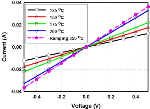
recombination terms at short circuit condition as function of the annealing time. For high band tail states, Langevin recombination can be neglected whereas for optimized

In this contribution, we report on the optimization of CIS and CIGS bottom cells, where we introduce promising high ‐ performance solar cells that have the poten- tial to be

[7], the data were analysed by introducing three time- (i.e. coverage-) dependent parameters: the binding energy ε, the sticking coefficient S, defined as the fraction of incident

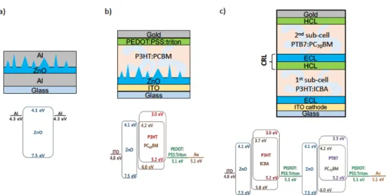
If we look at the energy diagram of various layers of our devices (as shown in Figure 2c)), shallow LUMO level of TPBi (2.7 eV) seems to introduce additional energetic barrier

QuickStep first runs the sequential program on representative in- puts (provided by a user or developer). For each input, it records the result that the program produces and

mg/kg, p.o.), significantly prevented the antinociceptive effect induced by the oral administration of Nauclea latifolia decoction (160 mg/kg) in both phases of