HAL Id: hal-02326982
https://hal.archives-ouvertes.fr/hal-02326982
Submitted on 31 Oct 2019
HAL is a multi-disciplinary open access
archive for the deposit and dissemination of sci-entific research documents, whether they are pub-lished or not. The documents may come from teaching and research institutions in France or abroad, or from public or private research centers.
L’archive ouverte pluridisciplinaire HAL, est destinée au dépôt et à la diffusion de documents scientifiques de niveau recherche, publiés ou non, émanant des établissements d’enseignement et de recherche français ou étrangers, des laboratoires publics ou privés.
High temperature properties of SiC and diamond
CVD-monofilaments
Georges Chollon, Roger Naslain, Calvin Prentice, Robert Shatwell, Paul May
To cite this version:
Georges Chollon, Roger Naslain, Calvin Prentice, Robert Shatwell, Paul May. High temperature prop-erties of SiC and diamond CVD-monofilaments. Journal of the European Ceramic Society, Elsevier, 2005, 25 (11), pp.1929-1942. �10.1016/j.jeurceramsoc.2004.06.013�. �hal-02326982�
Available at: https://doi.org/10.1016/j.jeurceramsoc.2004.06.013
HIGH TEMPERATURE PROPERTIES OF SiC AND DIAMOND CVD-MONOFILAMENTS
Georges CHOLLON, Roger NASLAIN
Laboratoire des Composites Thermostructuraux (LCTS), UMR 5801 (CNRS-SNECMA-CEA-UB1), Université Bordeaux 1, 3, allée de La Boétie, 33600, Pessac, France.
Calvin PRENTICE, Robert SHATWELL, QinetiQ, Cody Technology Park, Farnborough, Hampshire, GU14 0LX, UK.
Paul MAY, School of Chemistry, University of Bristol, Cantock’s Close, Bristol, BS8 1TS, UK.
KEY WORDS: Fibres, SiC, Diamond, Microstructure, Mechanical Properties
ABSTRACT
The chemical, structural and thermomechanical properties of SiC and diamond CVD-monofilaments have been investigated. Electron and Raman microprobe analyses showed graded radial atomic and phase distributions in the SiC filaments. Thermomechanical investigations (tensile/bending elastic modulus/creep tests) were carried out on single filaments and these properties were correlated with the physicochemical features. The thermal behaviour of the CVD-SiC filaments is strongly related to the nature and the amounts of intergranular secondary phases (free carbon or silicon). The strong covalent bonds and the microcrystalline state of the CVD-diamond filaments give rise to an outstanding thermal behaviour.
1 INTRODUCTION
Titanium matrix composites (TMCs) combine the high strength, stiffness and creep resistance of silicon carbide (SiC) monofilaments with the high ductility, toughness and corrosion resistance of titanium alloys. These high specific properties make TMCs highly innovative
materials for aeronautic engines, as their use in a bladed disc may yield a 55% weight reduction [1-2]. Unfortunately, a major obstacle to their industrial use is the high materials costs and the complexity of the manufacturing processes known to date (such as the foil-fibre-foil method or the electron beam physical vapour deposition (EB-PVD) tape/monofilament coating [1-3]).
An alternative and more affordable processing route is the liquid-state coating of the filament with Ti-alloy recently developed by Snecma-Moteurs [4]. This process is fast (the residence time of the fibres in the molten alloy is only of few tenths of a second) and high temperature (close to the Ti-alloy melting temperature); and it does, however, require particularly high strength and thermally stable monofilament reinforcement. This has led to the development of new monofilaments at the firm QinetiQ, the properties of which are discussed here.
High performance SiC monofilaments are prepared by chemical vapour deposition (CVD) on an electrically heated filament substrate. The market of CVD-SiC filaments is mainly shared by two companies; Specialty Materials Inc. (formerly Textron) in Lowell (USA) and QinetiQ (formerly DERA) in Farnborough (UK), providing, respectively, the SCS-6 and SM1140+ monofilaments. A small diameter tungsten wire (15 m) is used as the substrate by QinetiQ. Alternatively, a carbon wire of relatively large diameter (33 m) is used by Specialty Materials. The CVD-SiC sheath is deposited at about 1200°C from chloromethylsilanes in the presence of hydrogen and, in some cases, hydrocarbon species. The diameter of the SCS-6 filament is 140 m. The CVD-SiC sheath consists of a carbon rich SiC layer near the carbon core and a near stoichiometric SiC outer layer [5-6]. The filament is subsequently covered by a 3 m multilayered pyrocarbon-based coating. The diameter of the SM1140+ filament is 105 m. The CVD-SiC coating is stoichiometric near the tungsten core and silicon-rich in the outer part [7].
Alternatively, CVD-diamond filaments are very attractive candidates for TMCs reinforcement [8-9]. Current diamond growth rates achieved by plasma enhanced CVD (CVD) are still moderate as compared to those for CVD-SiC, but active research on diamond PE-CVD processing has recently given rise to promising advances [10]. PE-CVD-diamond filaments display outstanding Young’s modulus values, close to that for bulk diamond (1200 GPa) [9]. Moreover, they are expected to show a very high creep resistance and maintain their stiffness up to high temperatures in inert conditions, as long as graphitization does not occur (T>1600°C in vacuum or argon).
This paper reports a detailed and comparative study of the chemical, structural and thermomechanical properties of commercial and experimental CVD filaments. The objective is to evaluate the compatibility of the filaments with the liquid coating process and, for a better
understanding and modelling of the Snecma-Moteurs process (e.g. the calculation of the thermal residual stresses), to acquire various thermomechanical data within a wide temperature range.
2 MATERIALS
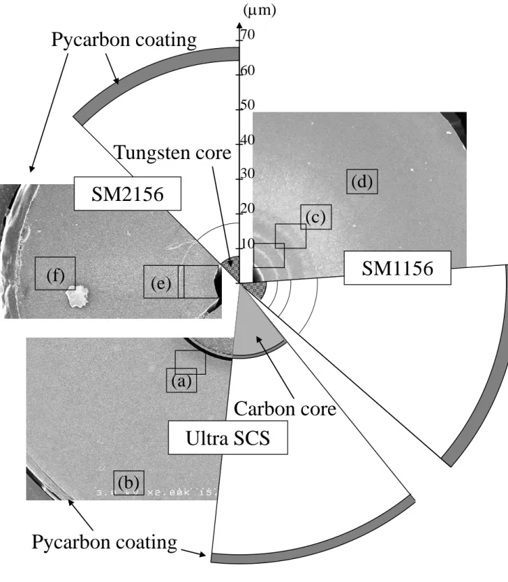
Four types of CVD-SiC filaments have been studied: SCS-6 and Ultra SCS from Speciality Materials Inc. and SM1156 and SM2156 from QinetiQ (table 1). The Ultra SCS is an upgrading of the SCS-6. It is reported to have a significantly higher failure strength [11]. The SM1156 filament is an early development version similar to the commercial SM1140+ but with an outer diameter of 147 m instead of 105 m (Fig. 1). The SM2156 filament is a recent material from QinetiQ, now undergoing production trials. In order to reduce the amount of free silicon co-deposited with SiC, to subsequently improve the stiffness and thermal stability of the filament, hydrocarbon species were added to the dichloromethylsilane/hydrogen mixture used for the SM1140+ or SM1156 filament [7]. SM2156 is 140m in diameter and has a tensile strength between 4 – 5GPa.
The CVD-diamond filament was processed at the University of Bristol. The diamond coating was deposited on a tungsten wire (50 m in diameter), in a hot filament CVD reactor using 1% methane in hydrogen as the precursor gas mixture [9]. The outer diameter of the resulting W/diamond filaments ranges from 120 to 150 m (i.e. 82-89 vol.% diamond) (Fig. 2). 3 EXPERIMENTAL
The morphology and the microstructure of the filaments were characterised with a field emission gun scanning electron microscope (FEG-SEM) (Hitachi S-4500, Japan).
The local chemical composition of the filaments was determined by electron probe microanalysis (EPMA) (SX 100 from CAMECA, France). The analyses were conducted on polished cross-sections of filaments. EPMA measurements were performed in the wavelength dispersion mode (10 kV, 10 nA), with a thallium acid phthalate (TAP) crystal analyser for Si-K and a large multilayer pseudo-crystal analyser (LPC2) for C-K. A SiC single crystal was used as standard. The spatial resolution was of the order of 1 to several m3. Linescan data were recorded along the radius of the filaments with a 2m stage step.
Raman microspectroscopy (RMS) is very useful to examine the microstructure of the filaments at the micrometer scale [12-14]. RMS analyses (LABRAM 010 from Dilor, France)
were carried-out on the same samples as those for EPMA. The excitation source was the 633 nm emission line of a He/Ne laser. The power was kept below 0.5 mW to avoid heating of the sample. The objective of the microscope (100) allowed a lateral resolution of the laser probe close to 1 m (the depth resolution being of the order of one to several hundreds of nanometers, depending on the material). As for EPMA, linescan measurements were recorded along the diameter of the fibres.
The diameter of the filament (d0) was measured by SEM and laser interferometry. Tensile
tests were carried out at room temperature to measure the Young’s modulus of the monofilaments. Owing to the high stiffness of the samples, the assessment of strain was examined with a particular attention. A direct strain measurement device was used (to avoid any compliance effect), derived from a commercial extensometer modified to allow the connection to the filament (L0=30 mm) (see Appendix, Fig. A1).
Longitudinal thermal expansion measurements were performed with a thermomechanical analyser device (TMA SETSYS 2400, from Setaram, France) specifically developed for the tensile testing of single filaments (L0 = 20 mm, F = 210-2 N) (Appendix, Fig. A2). The thermal
strain (L(T)=L(T)/L0) and the coefficient of thermal expansion (CTE, L=dL/dT) were
recorded versus temperature on both heating and cooling of the samples under argon (105 Pa) up to 1600°C (10°C min-1). A standard graphite specimen (AXM5Q from POCO Graphite) was used to correct the thermal expansion and the method was firstly validated by testing a tungsten wire.
Three-point bending tests were performed with a specific thermomechanical testing device (TMA SETSYS 2400, Setaram) on single filaments, at room and high temperature in argon (105 Pa) (Appendix, Fig. A3). These tests allowed both the measurements of the bending modulus versus the temperature and the flexural creep. The specimens were all loaded with a l0 =
12 mm-span alumina device. Both the applied load (F, F < 310-2 N) and the filament deflection
(y) were recorded versus time and temperature with a high resolution (10-4 N and 4 nm, respectively). The bending modulus (Ebend) and both the maximum strain (max) and applied stress
(max) at the surface of the filament were calculated from the load (F) and the deflection (y)
assuming the ideal three point bending theory (thin and homogeneous cylinder, low deflection...).
F d l 3 0 0 max 8 y l d 2 0 0 max 6 y F d l Ebend 4 0 3 0 3 4
Bend stress relaxation (BSR) tests were conducted on the filaments in argon (105Pa) at
temperature T (T=1000-1500°C). The samples were set in a graphite tool imposing a constant curvature R0 and heat treated for 1 h [15]. The thermal behaviour of the samples is characterised
by the stress relaxation ratio m = 1-(R0 / R), where R0 and R are respectively the initial and final
curvature of the filaments (R0 = 60 and 150 mm for the SiC and diamond filaments, respectively).
4 RESULTS AND DISCUSSION
4-1 Chemical and structural analyses
SCS-6 filament
Linescan EPMA data along the cross-section of the CVD-SiC coating of the SCS-6 filament are shown in figure 3. This filament displays a free carbon excess of about 5 at.% from the interface with the carbon core to about 20 m. The free carbon concentration suddenly decreases and stabilises to a near stoichiometric composition (with a slight silicon excess) along the last part of the coating up to the CVD-SiC/pyrocarbon coating interface.
From SEM observations, the CVD-SiC sheath consists of two main distinct parts, the first layer being actually composed of three intermediate layers [5-6, 11]. The main inner coating has a fine microstructure whereas the outer part is significantly coarser, with radial columnar grains.
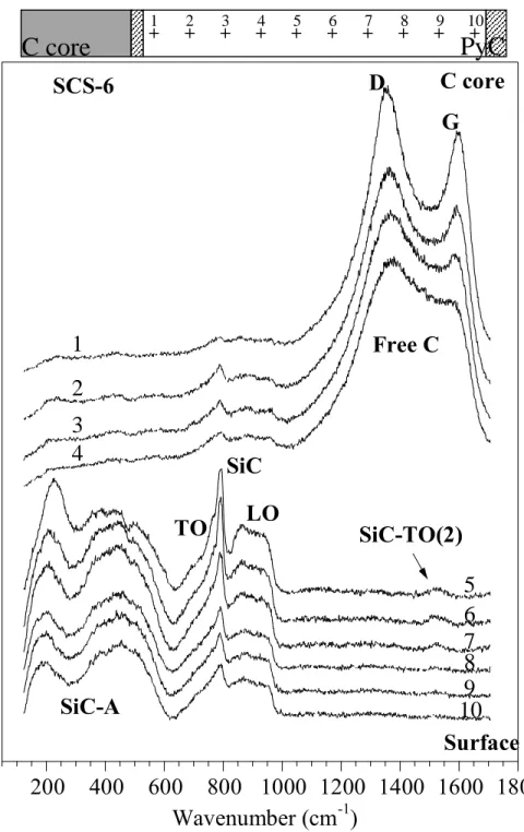
Figure 4 shows the Raman spectra recorded along the radius of the SCS-6 filament. As already mentioned by other authors, the first spectra recorded along the inner CVD-coating near the carbon core show simultaneously crystalline SiC and free aromatic carbon features [12-14]. This is in good agreement with the EPMA profile and confirms the coexistence of both the SiC and free carbon phases. The two broad bands at 1600 cm-1 and 1350 cm-1 are assigned respectively to the G peak with the E2g symmetry, characteristic of graphite (involving vibrations
within the graphene sheets) and to the D peak (generally associated with a broadening of the G peak) characteristic of polycrystalline or disordered carbons [16-17]. The SiC Raman features appear within the 600-1000 cm-1 (optical modes) and the 200-600 cm-1 (acoustical modes) regions. In the pure cubic -SiC polytype, only two sharp and well defined transverse optical (TO) and longitudinal (LO) phonons are expected, respectively, at 796 and 972 cm-1 [18]. In the present case, the occurrence of acoustic features and of the two broad components in the optical region point out a heavily faulted -SiC structure involving grain boundaries and a high density of stacking faults [14]. Consistently with the EPMA profiling, the carbon Raman features
suddenly vanish within the outer part of the coating (Fig. 4). The faulted -SiC phase is the only one observed, the intensity of the TO peak slightly decreasing outward, owing to the decrease of the SiC grain size. It is worthy of note that although free silicon is not evidenced in the outer part of the as-processed filament, it was detected in small amounts as a weak, sharp peak at 520 cm-1 after re-crystallisation at 1400°C.
Ultra SCS filament
The radial elemental composition of the Ultra SCS filament differs from that of the SCS-6. The carbon concentration is significantly higher near the carbon core (about 20 at.% of free carbon) (Fig. 5). There is a gradual decrease in free carbon with radius, the bulk of the fibre being essentially stoichiometric SiC. The carbon concentration slightly increases again near the surface of the filament (4 at.% of free carbon).
Whereas the SCS-6 filament shows a pronounced transition in the microstructure of the CVD-SiC sheath, the SCS Ultra exhibits a relatively regular and fine-grained microstructure throughout the whole SiC layer (Fig. 6). The first deposit apparently consists of very fine nanocrystallites. A radially oriented columnar structure gradually appears at increasing distance from the core, with grains up to about 1 m long at approximately 10 m from the core. The columnar shape of the SiC crystallites is still observed along the rest of the deposit but their size gradually decreases until the surface of the filaments. Such features agree well with a previous TEM investigation [19], although an homogeneous microstructure with relatively equiaxial SiC grains was also described by other authors [11].
The Raman spectrum recorded from the carbon core/CVD-SiC interface shows simultaneously disordered carbon (the G and D bands at 1350 and 1600 cm-1) and faulted -SiC (TO and LO peaks respectively at 793 cm-1 and 967 cm-1) features (Fig. 7). The presence of very intense G and D bands, together with weak and broad SiC peaks near the carbon core/CVD-SiC interface, is indicative of a large excess of free carbon and a small SiC grain size [11]. In agreement with the EPMA data, the intensity of the carbon bands rapidly decreases (and the intensity of the SiC peaks increases) away from carbon core. The G and D bands broaden and combine to a weak and wide single band (1100-1700 cm-1) in the central part of the SiC layer, which is characteristic of a very disordered form of carbon. The intensity of the carbon band slightly increases again near the surface, confirming the free carbon enhancement evidenced by EPMA. The LO peak is significantly more intense, both the TO and LO peaks are sharper and the acoustic modes (around 300-650 cm-1) are much less intense in the central part of the Ultra SCS
CVD-layer than in the outer part of the SCS-6 filament. Such features suggest a better crystalline state of the CVD-SiC (i.e. closer to -SiC) and/or a likely different microstructure, as compared to the highly oriented columnar texture of the SCS-6 outer sheath [11, 14]. This microstructure may be related to the presence of free carbon at the SiC grain boundaries. This could lead to smaller crystallites and some deviation from the usual textured CVD structure [14]. As already suggested by the SEM analyses, the slight decrease in intensity (and increase in width) of both the TO and LO peaks from the inner to the outer part of the SiC sheath, supports a gradual reduction of the crystallite size during deposition.
SM1156 filament
The SM1156 filament consists of stoichiometric SiC near the tungsten core only (Fig. 8). The silicon concentration gradually increases outwards to reach a free silicon excess of about 10 at.%.
Very large radial columnar grains are found at the W/CVD-SiC interface of the SM1156+ filament (Fig. 9). The central part of the etched filament shows an irregular concentric morphology due to interruptions of the CVD-grain growth. The microstructure becomes gradually finer outwards until the surface, with no apparent texture at the outer part of the CVD-layer, as evidenced by FEG-SEM (Fig. 9).
A particularly sharp and intense SiC-TO peak (790-800 cm-1) is observed near the
tungsten core, indicating a SiC highly crystalline state (Fig. 10). The spectrum also shows very broad additional features within both the optical and acoustical regions, typical of a heavily faulted -SiC structure (grain boundaries, stacking faults). The absence of a well defined LO mode (which is observed in the Ultra SCS) is related to the preferential orientation of the (111) crystallographic planes parallel to the CVD-SiC coating (i.e. to the fibre axis) which is equivalent, in the present case, to the Raman scattering direction. The SiC-TO feature broadens and weakens rapidly outwards, showing a strong decrease of the SiC grain size from micro to nanocrystallites (as shown by the SEM analysis). An additional broad band at 400-550 cm-1 appears while reaching the outer part of the filament, which is assigned to a large amount of amorphous free silicon (as suggested by EPMA).
SM2156 filament
The SM2156 filament shows a slight carbon excess (about 8 at.% of free carbon) close to the tungsten core (Fig. 11). EPAM indicates the free carbon amount fluctuates slightly along the
first 20 m of the coating. The composition remains almost stoichiometric throughout the rest of the CVD-sheath, though with a very slight carbon excess.
The microstructure of the SM2156 filament is very similar to that of the Ultra SCS, but with a smaller SiC grain size (Fig. 12). The initial coating is nanocrystalline and radial columnar sub-micrometer grains appear at increasing distance from the core. A discontinuity in the CVD growth is observed at about 10m from the core interface. The columnar shape of the SiC crystallites is still observed along the rest of the deposit but their size progressively decreases until the surface.
As in the central part of the Ultra SCS CVD-coating, the Raman carbon features are visible near the W core/CVD-SiC interface as a single broad band at 1100-1700 cm-1, characteristic of a very disordered form of carbon (Fig. 13). The evolution of the intensity of this band along the radius is consistent with the free carbon concentration obtained by EPMA. The SiC phase appears rather well crystallised, though in a more faulted form than in the Ultra SCS. As in the Ultra SCS, no free silicon (400-550 cm-1) is detected throughout the filament.
CVD-diamond filament
Whereas all the CVD-SiC filaments have smooth surfaces and relatively fine microstructure, the CVD-diamond deposit is rough and highly textured with large columnar microcrystals (Fig. 2). Raman spectra recorded along the cross-section of the diamond coating are rather similar. In addition to an intense photoluminescence background, the spectra clearly show the sharp diamond characteristic peak (triply-degenerate optical phonon) at about 1335 cm-1 (Fig. 14). The peak position changes slightly, probably because of local stress variations [9].
4-2 Thermo-mechanical analyses Elastic modulus
All the filaments show a linear and brittle behaviour in tension. The average Young’s modulus (as measured in tension) of the various filaments (Etens) is shown in Table 1. The
Young’s modulus of the three CVD-SiC filaments currently ranges from 330 to 385 GPa whereas it is as high as 930 GPa for the CVD-diamond filament. Using the Rule of Mixtures, the modulus of the CVD-diamond coating alone reaches 1030 GPa, close to the theoretical value for bulk diamond (1200 GPa) [8]. The bulk modulus of pure SiC is generally accepted to be close to 450 GPa. The lower values obtained from the CVD-SiC filaments are partly due to the contribution from the outer pyrocarbon coating, the core and the CVD-SiC coating itself, i.e. the microstructure of the SiC phase as well as the presence of possible secondary phases. The
SM1156 filament shows a modulus significantly lower than those of the near-stoichiometric SM2156 and Ultra SCS filaments. Such a low value is undoubtedly due to the rather high amounts of free silicon in the former (Esi = 190 GPa, for an average silicon fraction of about 5
vol.%). The Young’s modulus of the SCS-6 filament is intermediate, with a value in-between those of the silicon-rich and the two near stoichiometric filaments. The lower stiffness of the SCS-6 filament is likely related to the free carbon phase co-deposited with SiC within the inner region of the CVD-layer.
The bending modulus (Ebend) of the various filaments is also reported in Table 1. Ebend is
rather characteristic of the near-surface part of the filament which is more stressed in bending than the core. This is indeed the case for the 50 m core CVD-diamond filament, where the bending modulus is closer to the value expected for bulk diamond. The contribution of the thicker pyrocarbon coating is also thought to be responsible for the lower bending modulus of both SM1156 and SM2156 as compared with that of SCS-6 and Ultra SCS. Ebend may be also affected
by the chemical and structural gradient along the CVD-SiC layer itself. The presence of a more compliant layer located either near the core (the free carbon rich layer in SCS-6) or near the surface (the free silicon rich layer in the SM1156), respectively, results in a higher or lower value of Ebend with respect to Etens.
The evolution of the bending modulus versus test temperature is shown in Fig. 15. A decrease of Ebend is observed with increasing T for all the filaments, but to a considerably
different extent. The CVD-diamond and the nearly-stoichiometric CVD-SiC filaments show the best thermal stability. The CVD-diamond material has strong sp3 covalent bonds and a large grain size. It therefore shows only a very limited decrease in stiffness with temperature. The slight drop of Ebend with T in this case may be assigned essentially to the contribution of the 50 m tungsten
core and to a minor superficial graphitisation (as observed by RMS) occurring at high temperature. The Ultra SCS filament shows the best thermal behaviour of all the CVD-SiC specimens. This is not only due to its nearly stoichiometric composition but also, to the existence of the free carbon phase. Free carbon as an intergranular phase is expected to show better thermal stability than free silicon (melting point = 1410°C). The detrimental effect of intergranular free silicon upon the elastic modulus is clearly noticeable for the SCS-6 filament [20], in which the slightly silicon-rich CVD-SiC layer is located at the highly stressed outer part. A similar but much more accentuated phenomenon is apparent for the SM1156 filament which contains higher amounts of free silicon near the surface.
The longitudinal thermal expansion of the SCS-6 filament has already been investigated by several authors [21-23]. The thermal expansion (L) of all the filaments is presented in figure
16.
The thermal behaviour of the SCS-6 filament is similar to that previously reported in literature [21-23]. L increases almost linearly from room temperature up to 1600°C (with an
average CTE value of L = 5.15 10-6 K-1 within T = 200-1000°C), except a slight and sudden
shrinking around 1350-1400°C. This phenomenon is reversible but slightly delayed on cooling (1350-1280°C). It is assigned to the fusion of the small amounts of free silicon present in the outer CVD-SiC layer, as evidenced by RMS after annealing [12].
The thermal behaviour of the SM1156 filament shows a similar reversible shrinkage at about 1350-1420°C but with a significantly higher amplitude. L is also close to 5 10-6 K-1, a
typical value for stoichiometric SiC (L = 5.1 10-6 K-1 for T=200-1000°C), on both heating and
cooling. Such shrinkage phenomenon on heating (expansion on cooling, respectively) is unambiguously due to the presence of large amounts of free silicon (10 at.%) in the outer CVD sheath of this filament.
The SCS Ultra and the SM2156 filaments both show a linear and almost entirely reversible thermal expansion behaviour within the whole tested temperature range. Such a behaviour is consistent with the absence of free silicon, as evidenced above by the chemical and structural analyses. The coefficient of thermal expansion is respectively equal to 5.1 and 5.2 10-6
K-1 within T = 200-1000°C for both filaments. A minor evolution of L is however noticed
beyond 1250°C for the SM2156 filament and 1400°C for the Ultra SCS filament. This phenomenon is not reversible (as opposed to the discontinuity due to the presence of free silicon) and might be related to a structural evolution of the material, e.g. a possible ordering of the free carbon phase at high temperature.
The diamond filament also displays a quasi-linear and reversible thermal expansion. This behaviour is indicative of the apparent thermal stability of the CVD-diamond coating in inert atmosphere up to 1600°C. As expected, the CTE is significantly lower than that of the SiC-based filaments. It increases continuously with the temperature, from 3 10-6 K-1 at 200°C, to 3.8 10-6
K-1 at 1400°C. The CTE of bulk diamond at room temperature is generally accepted to be of the order of 1-2 10-6 K-1. It is reported to increase significantly with temperature (e.g.
L = 1 10-6 K -1 at 20°C and
L = 5.1 10-6 K-1 at 1130°C) [24]. Such a thermal expansion discrepancy observed
between pure bulk diamond and the CVD filament might be related to the structural defects evidenced by RMS.
Bending stress relaxation and bending creep
The thermal evolution of the BSR parameter m is presented in figure 17. A smaller curvature (R0=150 mm) had to be applied to the CVD-diamond filament owing to its lower
fracture strain. For comparison, the same conditions were also used for the CVD-SiC filaments. The R0 value and therefore, the applied surface strain (s d0/2R0), has a minor influence on m
for the SiC filaments at 1500°C (Fig. 17) [25]. The BSR resistance of the SM1156 filament is significantly lower than that of the SCS-6 (about 250°C lower for a given m value), while they show similar thermal activation [25]. The Ultra SCS and SM2156 filaments show a BSR resistance improvement of about 150°C with respect to the SCS-6 and a slightly lower thermal activation.
The CVD-diamond filament displays the best BSR resistance of all the tested filaments, i.e. at least 250°C higher than SM2156.
The bending creep behaviour of the various filaments is compared at 1200 and 1400°C (=300MPa) (Fig.18a-b). Short partial unloading cycles (300-30 MPa) were carried out during the creep tests to minimise the effect of friction forces and to measure the residual strains and the bending moduli. All the CVD-SiC filaments show only primary creep at 1200°C within the studied time range. The correlation between the creep behaviour and the composition/microstructure of the various filaments is particularly apparent. Both the near stoichiometric CVD-SiC filaments (Ultra SCS and SM2156) show a similar and particularly high creep resistance. The creep strain of the SCS-6 filament is about twice that of Ultra SCS and SM2156, whereas the SM1156 strain is about fifteen times that of SM2156. The discrepancy between the various CVD-SiC filaments is even more pronounced at 1400°C. The SCS-6 creep strain rate is at least five times higher than that of the Ultra SCS and SM2156 and the creep strain rate of the SM1156 filament was so high when loaded that it failed after only few minutes (the creep behaviour of the SM1156 filament was therefore not studied beyond 1200°C).
The bending creep behaviour of the various CVD-SiC filaments was investigated as a function of the temperature (900-1400°C) and the load (max = 150-900 MPa). For all the
filaments and almost the whole temperature range the maximum creep strain versus time (t) can be experimentally described by a simple power law: max(t) = Ctp, where C and p are numerical
constants. Such a bending creep time dependence is similar to the tensile creep law generally proposed for the SCS-6 filament; i.e. a function of the temperature-compensated time = t
exp(-Q/RT)) (where Q is the activation energy and R the universal gas constant R = 8.3144 Jmol-1K-1)
and a power of the applied stress . The corresponding expression of the creep strain is [26-27]:
) exp( ) ( 0 RT pQ t A t pn
where A0 is a constant, p, the time power exponent and n, the stress exponent. When the
CVD-SiC filaments are tested in tension, using temperature and stress conditions similar to those examined here, the creep strain is usually less than 1%, a steady-state creep is never observed and the stress exponent n is very close to 1, a feature suggesting that the creep mechanism is controlled by diffusion [26-27]. The time and temperature dependence of the bending creep strain can therefore be described by the same above equation, provided that n 1. For all tested filaments, the bending creep curves recorded for various temperature and stress levels were fitted to simple power law: max(t) = Ctp. The time exponent p was determined for each type of filament
by averaging the best-fit time power laws (table 2) and the ln C values were plotted as a function of ln and 1/T (Fig. 19-20) to determine respectively the stress exponent (n), the activation energy (Ea) and the pre-exponential constant (A0), (Ea, table 2).
Figures 18-20 confirm the significant influence of the chemical/microstructural features on the creep resistance of the various filaments. As presumed above, and already stated by other authors for similar materials, the bending creep stress exponent is very similar for all tested filaments and near unity (Fig. 19), suggesting a diffusion controlled creep mechanism.. The activation energies of the SCS-6 and SM1156 filaments are very close within the temperature range 1000-1100°C (456-466 kJ mol-1, Table 2, Fig. 20). The creep rate of the near stoichiometric
filaments is less temperature dependent, especially at low temperature. The SM2156 filament shows two distinct temperature domains with a transition at 1200°C (Q= 239 kJ mol-1 for T 1200°C and Q= 410 kJ mol-1 for T 1200°C) (Table 2, Fig. 20). The activation energies of the SCS-6, SM1156 and both the Ultra SCS and SM2156 filaments at high temperature, are all near the range of the silicon or carbon grain boundary self-diffusion (respectively 612 kJ mol-1 and 554 kJ mol-1 [27-28]), suggesting a common creep behaviour involving grain boundary sliding and controlled by grain boundary diffusion [25-26]. Their significantly different creep rates can be explained by the SiC grain size, as well as the nature of the grain boundary and particularly of the intergranular phase. The grain boundary sliding leads to intergranular normal stresses. The creep rate is, therefore, strongly related to the accommodation of the intergranular phase. The
poor creep resistance of the SM1156 filament is obviously related to the particularly large excess of amorphous free silicon (Tf = 1410°C) and to the smaller SiC grain size of the outer layer
(predominantly stressed in bending). Conversely, as already established for an other experimental filament from Textron (SCS-X), the better thermal resistance of both the Ultra SCS and SM2156 filaments can be assigned to the presence of co-deposited free carbon [29]. The small amount of intergranular carbon hinders the grain sliding and therefore improves the creep resistance. Such a disordered aromatic carbon phase has considerably better creep resistance than amorphous silicon. It is, however, likely to be subject to a slight structural evolution activated at temperatures close to or beyond that of the CVD process. This irreversible phenomenon might be responsible for the change of the activation energy occurring at 1200°C in the case of the SM2156 filament.
Primary creep is observed for all the filaments, at least at the initial loading stage. This behaviour might be assigned to concurrent SiC grain growth (the creep parameters indeed suggest a grain-boundary diffusion mechanism) and/or to load sharing due to the multilayered composite structure of the SiC-CVD filaments [25]. Steady state creep is never observed for the free silicon rich filaments for the studied time range, whereas it appears only after a sufficient duration (t > 104 s) in the case of the Ultra SCS and SM2156 filaments. Raman analyses evidenced a significant SiC grain growth in the former, whereas crystallisation was strongly inhibited by the presence of the intergranular free carbon phase in the latter. Although the contribution of load sharing can not be excluded, the structural changes of the both the silicon carbide and the free carbon phases are likely to contribute extensively to transient creep. These effects have not been investigated in detail here because of the complexity of the flexural loading analysis.
The CVD-diamond filament exhibits a considerably higher creep resistance than the CVD-SiC filaments (Fig. 18b). Despite the large 50 m W core, the creep strain is less than 1/10 that of the SM2156 filament. The strong C-C covalent bond, the large grain size and the absence of low melting temperature and/or compliant intergranular phase, are responsible for the exceptional thermal behaviour of the diamond filament. Besides the creep strain, the unloading cycles evidenced a slight and constant decrease of the bending modulus versus time. This phenomenon might be related to the superficial degradation of the CVD-diamond at high temperature, as shown by RMS.
5 CONCLUSION
The SCS-6 filament consists of a free carbon-rich inner layer and a near stoichiometric outer layer, with a slight silicon excess. The SM1156 filament composition is stoichiometric near
the tungsten core and turns to a large silicon excess (10 at.%) near the surface. The SM2156 monofilament is carbon-rich near the core and near stoichiometric with a slight amount of free carbon all along the CVD-SiC sheath. . Ultra-SCS is similar, having slightly more free carbon distributed within the SiC. All these filaments contain sub-micron SiC crystals, with decreasing grain size when increasing the amount of the secondary phase. The CVD-diamond filament shows an homogeneous microcrystalline structure.
The thermomechanical behaviour of the CVD-SiC filaments (tensile or bending modulus and creep) depends on their radial composition and microstructure. The room temperature stiffness increases with decreasing amounts of compliant secondary phases (free carbon or silicon). The presence of intergranular free carbon results in an elastic modulus stable at high temperature and an improved creep resistance. By contrast, free silicon leads to a catastrophic drop of high temperature stiffness and creep resistance. The high temperature bending tests have shown that the filaments undergo essentially primary creep, especially in the case of the free silicon rich filaments. The transient creep of the free carbon containing filaments eventually changes to a steady state process at high temperature (T1400°C). The creep parameters (n, Ea)
suggest a grain boundary diffusion mechanism. The increase of the amount of intergranular free silicon leads to a catastrophic creep rate whereas the presence of free carbon improves the creep resistance considerably. The transient behaviour is likely to be a consequence of the simultaneous SiC grain growth and the ordering of the free carbon phase. It might also be related to load redistribution due to the multilayered composite structure of the SiC filaments. The CVD-diamond filament displays exceptional stiffness and creep behaviour up to high temperatures due to the strong C-C covalent bonds, the large grain size and the absence a low melting temperature and/or compliant intergranular phase. If the growth rate and the failure strain could be increased to reasonable levels, such filament may find uses as CMM or CMC reinforcements.
ACKNOWLEDGEMENTS
The authors would like to thank Speciality Materials Inc. for the supply of filaments. They are also greatly indebted to M. Lahaye from CeCaMa, Pessac as well as M. Couzi and J.L. Bruneel from LPCM, Talence for fruitful contribution to the EPMA and RMS analyses, respectively.
Specific devices were developed for the thermo-mechanical testing of the CVD-monofilaments. Tensile tests were carried out at room temperature with a standard tensile testing apparatus to measure the Young’s modulus. The strain was directly calculated from the elongation of the filament (to avoid any compliance effect), with a commercial extensometer that had been modified to allow the connection to the filament (Fig. A1). The filament was connected to the extensometer by means of two tinned copper clamps (to avoid any damage and early rupture of sample). Both the thermal expansion and the bending high temperature tests were carried-out with a thermomechanical analyser (TMA SETSYS 2400, from Setaram, France). A graphite device was specifically designed by Setaram for the longitudinal thermal expansion analysis of the monofilaments in tension (Fig. A2). A compact alumina three-point bending system was used for the high temperature modulus and creep tests (Fig. A3).
REFERENCES
[1] C.M. Ward-Close, J.G. Robertson and S.P. Godfrey, “Fabrication of Monofilament Reinforced Titanium” in Comprehensive Composite Materials, A. Kelly and C. Zweben eds.-in-chief, Vol. 3: Metal Matrix Composites, T.W. Clyne ed., Pergamon, Elsevier Science Ltd. (2000) 655-678.
[2] C. Leyens, J. Hausman and J. Kumpfert, “Continuous Fiber Reinforced Titanium Matrix Composites: Fabrication, Properties and Applications”, Adv. Eng. Mater. 5 [6] (2003) 399-410. [3] C.M. Ward-Close and C. Loader, “PVD Processing of Fibre Reinforced Composites” in Recent Advances in Titanium Metal Matrix Composites, F.H. Froes and J. Storer eds., The Minerals, Metals and Materials Society (1995) 19-32.
[4] B. Dambrine, M. Garnier, J. Hamburger, Y. Honnorat, L. Molliex, J. Feigenblum and G. Weiss, “Method for Metal Coating of Fibres by Liquid Process”, US Patent No.: US 6,174,570, B1, Jan. 16, 2001.
[5] X.J. Ning and P. Pirouz, “The microstructure of SCS-6 fiber”, J. Mater. Res. 6 (10) (1991) 2234-2248.
[6] X.J. Ning, P. Pirouz, K.P.D. Lagerlof and J. DiCarlo, “The Structure of Carbon in Chemically Vapor Deposited SiC Monofilaments”, J. Mater. Res. 5 (12) (1990) 2865-2876.
[7] T.T. Cheng, P. Doorbar, I.P. Jones and R.A. Shatwell, “The microstructure of Sigma 1140+ SiC fibres”, Mat. Sci. Tech., A260 (1999) 139-145.
[8] P.W. May, “CVD Diamond: a New Technology for the Future?”, Endeavour 19 [3] (1995) 101-106.
[9] E.D. Nicholson, J.R. Weeks and M.N.R. Ashford, “The Effect of Varying Deposition Conditions on the Young’s Modulus of Diamond Coated Wires”, Diamond and Related Materials 6 (1997) 817-821.
[10] K.L. Choy, “Chemical Vapour Deposition of Coatings”, Progress in Materials Science 48 [2] (2003) 57-170.
[11] P.R. Smith, M.L. Gambone, D.S. Williams and D.I. Garner, "Heat Treatment Effects on SiC Fiber", J. Mater. Sci., 33 (1998) 5855-5872.
[12] J. Kim, S. Tlali, H.E. Jackson, J.E. Webb and R.N. Singh, “A Micro-Raman Investigation of the SCS-6 Fiber”, J. Appl. Phys. 82 [1] (1997) 407-412.
[13] P. Colomban, “Raman Microspectrometry and Imaging of Ceramic Fibers in CMCs and MMCs” in “Advances in Ceramic-Matrix Composites V”, Ceramic Trans. vol. 103, N.P. Bansal, J.P. Singh and E. Ustundag eds., The American Ceramic Society (2000) 517-540.
[14] Y. Ward, R.J. Young and R.A. Shatwell, “A Microstructural Study of Silicon Carbide Fibres through the use of Raman Microscopy”, J. Mater. Sci. 36 (2001) 5566.
[15] G.N. Morsher and J.A. DiCarlo, “A Simple Test for Thermomechanical Evaluation of Ceramic Fibers”, J. Am. Ceram. Soc. 75 [1] (1992) 136-140.
[16] F. Tuinstra and J.L. Koenig, “Raman Spectrum of Graphite”, J. Chem. Phys. 53 [3] (1970) 1126-1130.
[17] A. Cuesta, P. Dahmelincourt, J. Laureyns, A. Martinez-Alonzo and J.M.D. Tascon, “Raman Microprobe Study on Carbon Materials”, Carbon 32 [8] (1994) 1523-1532.
[18] D.W. Feldman, J.H. Parker Jr, W.J. Choyke, and L. Patrick, “Phonon Dispersion Curves by Raman Scattering in SiC Polytypes 3C, 4H, 6H, 15R and 21R”, Phys. Rev. 173 [3] (1968) 787-793.
[19] K. Dyos, "Microstructural Analysis of a Variety of SiC Monofilaments", unpublished DERA report n°DERAMSS2CR9802401.0, July 1998.
[20] R.C. Warren, C.D. Weaver and S.S. Sternstein, “Dynamic and Transient Characterization of Silicon Carbide Fibers at Elevated Temperatures” Proc. of ICCM-11, vol. 4, M.L. Scott ed., Woodhead Publishing Ltd., (1997) 633-642.
[21] M.K. Brun, M.P. Borom, Thermomechanical properties of chemically vapor deposited silicon carbide filaments, J. Am. Ceram. Soc. 72 (10) (1989) 1993-1996.
[22] A. Elkind, M. Barsoum, P. Kangutkar, “Thermal expansion of silicon carbide monofilaments and silicon carbide-borosilicate composites”, J. Am. Ceram. Soc. 75 (10) (1992) 2871-2873.
[23] E. Lara-Curzio, S.S. Sternstein, C.R. Hubbard, B. Cavin and W. Porter, “High Temperature Structural Stability of Chemically Vapor-deposited Silicon Carbide Filaments”, Mater. Sci. Eng. A172 (1993) 167-171.
[24] The American Institute of Physics Handbook, 3rd Edition, D.E. Gray ed., McGraw Hill
(1972).
[25] G.N. Morsher, C.A. Lewinson, C.E. Bakis and R.E. Tressler, “Comparison of Bend Stress Relaxation and Tensile Creep of CVD SiC Fibers”, J. Am. Ceram. Soc. 78 [12] (1995) 3244-3252.
[26] C.A. Lewinson, L.A. Giannuzzi, C.E. Bakis and R.E. Tressler, “High-Temperature Creep and Microstructural Evolution of Chemically Vapor-Deposited Silicon Carbide Fibers”, J. Am. Ceram. Soc. 82 [2] (1999) 407-413.
[27] M.H. Hon, M.F. Davis and D.E. Newbury, “Self-Diffusion of 30Si in Polycrystalline -SiC”, J. Mater. Sci. 15 (1980) 2073-2080.
[28] M.H. Hon and M.F. Davis, “Self-Diffusion of 14C in Polycrystalline -SiC”, J. Mater. Sci.
14 (1979) 2411-2421.
[29] J.C. Goldsby, H.M. Yun and J.A. DiCarlo, “Creep and Rupture of an Advanced CVD SiC Fiber”, Scripta Materiala, 37 [3] (1997) 299-303.
Table captions
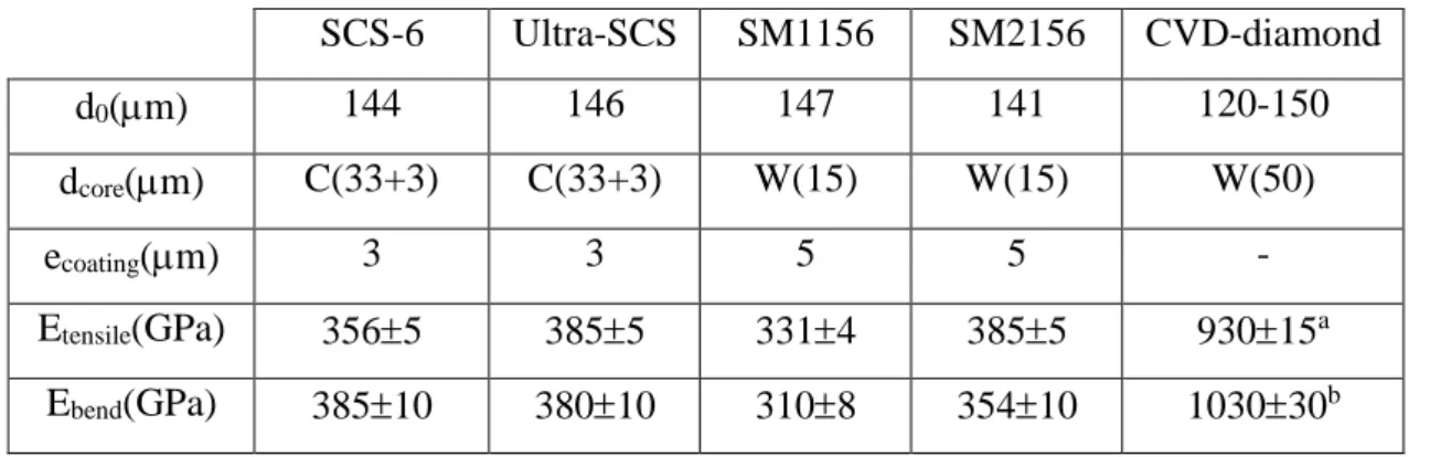
Table 1: Elastic modulus at room temperature of the filaments (a Øext=123 m, b Øext=143 m)
Tables SCS-6 Ultra-SCS SM1156 SM2156 CVD-diamond d0(m) 144 146 147 141 120-150 dcore(m) C(33+3) C(33+3) W(15) W(15) W(50) ecoating(m) 3 3 5 5 - Etensile(GPa) 3565 3855 3314 3855 93015a Ebend(GPa) 38510 38010 3108 35410 103030b
Table 1: Elastic modulus at room temperature of the filaments (a Øext=123 m, b Øext=143 m)
SCS-6 Ultra-SCS SM1156 SM2156
p 0.43 0.42 0.42 0.42
n 1.040.04 0.960.02 1.07 1.010.06 A0 2.1 10-7 1.5 10-8 6.2 10-7 4.2 10-11 a 1.4 10-8 b
Q(kJmol-1) 46610 37218 45618 23914 a 41033 b
Figure captions
Figure 1: Cross sections of the CVD-SiC filaments
Figure 2: SEM micrograph of the CVD-diamond filament
Figure 3: EPMA radial profile of the SCS-6 filament
Figure 4: RMS radial profile of the SCS-6 filament
Figure 5: EPMA radial profile of the Ultra SCS filament
Figure 6: SEM micrograph of the Ultra SCS filament
Figure 7: RMS radial profile of the Ultra SCS filament
Figure 8: EPMA radial profile of the SM1156 filament
Figure 9: SEM micrograph of the SM1156 filament
Figure 10: RMS radial profile of the SM1156 filament
Figure 11: EPMA radial profile of the SM2156 filament
Figure 12: SEM micrograph of the SM2156 filament
Figure 13: RMS radial profile of the SM2156 filament
Figure 14: Raman spectrum from the CVD-diamond filament
Figure 15: Bending modulus thermal behaviour of the filaments
Figure 17: BSR thermal behaviour of the filaments
Figure 18a: Bending creep behaviour of the filaments (T=1200°C)
Figure 18b: Bending creep behaviour of the filaments (T=1400°C)
Figure 19: Bending creep behaviour of the filaments (stress behaviour)
Figure 20: Bending creep behaviour of the filaments (temperature behaviour)
APPENDIX
Figure A1: Room temperature tensile testing device for Young’s modulus measurement (with direct strain measurement)
Figure A2: High temperature tensile testing device for longitudinal thermal expansion analysis
Figure A3: High temperature three-point bending device for for bending modulus and creep measurements