HAL Id: hal-02442466
https://hal.archives-ouvertes.fr/hal-02442466
Submitted on 16 Jan 2020HAL is a multi-disciplinary open access
archive for the deposit and dissemination of sci-entific research documents, whether they are pub-lished or not. The documents may come from teaching and research institutions in France or abroad, or from public or private research centers.
L’archive ouverte pluridisciplinaire HAL, est destinée au dépôt et à la diffusion de documents scientifiques de niveau recherche, publiés ou non, émanant des établissements d’enseignement et de recherche français ou étrangers, des laboratoires publics ou privés.
Growth optimization of columnar nanostructured
diamond films with high electrical performances for
SOD applications
M. Lions, S. Saada, M.-A. Pinault, F. Andrieu, O. Faynot, P. Bergonzo
To cite this version:
M. Lions, S. Saada, M.-A. Pinault, F. Andrieu, O. Faynot, et al.. Growth optimization of columnar nanostructured diamond films with high electrical performances for SOD applications. E-MRS sym-posium 2010 WIDE BANDGAP CUBIC SEMICONDUCTORS: FROM GROWTH TO DEVICES:, Oct 2010, Strasbourg, France. pp.129-132, �10.1063/1.3518278�. �hal-02442466�
AIP Conference Proceedings 1292, 129 (2010); https://doi.org/10.1063/1.3518278 1292, 129
© 2010 American Institute of Physics.
Growth optimization of columnar
nanostructured diamond films with high
electrical performances for SOD applications
Cite as: AIP Conference Proceedings 1292, 129 (2010); https://doi.org/10.1063/1.3518278
Published Online: 15 November 2010
Growth optimization of columnar nanostructured
diamond films with high electrical performances for SOD
applications
M. Lions
a,c, S. Saada
a, M.-A. Pinault
b, F. Andrieu
c, O. Faynot
c, P. Bergonzo
aa
CEA, LIST, Diamond Sensors Laboratory, F-91191 Gif-sur-Yvette, France. b
Groupe d’Etude de la Matière Condensée (GEMaC) - CNRS - Université Versailles St Quentin– 92195 Meudon Cedex, France.
c
CEA, LETI, MINATEC, F-38054 Grenoble, France. mathieu.lions@cea.fr
Abstract. In today’s nanoelectronics devices, thermal management is a major issue to miniaturization. Because of
its high thermal conductivity, diamond is an extremely interesting material for heat spreading. SOI (Silicon-On-Insulator) technology suffers of the poor thermal dissipation due to the silicon oxide buried layer. Thus, SOD (Silicon-On-Diamond) based on dielectrical diamond layer is seen as a promising candidate for future bulk solution. Polycrystalline diamond layers of extreme insulating properties (>1014 Ω.cm) are successfully synthesis
with thickness under 150 nm on 2 inches silicon wafer. However, defects due to the growth and the polycrystal structure are responsible for the detrimental current stimulate by alternative electrical field. The defects activation energies were measured on columnar nanostructured diamond grown under different conditions. Values of 0.56 to 1.56 eV were found for defects in these films and were correlated to the growth parameters as well as the diamond morphology.
Keywords: Diamond, SOD, Nanocrystalline material, MPCVD, Crystal defects, Electrical properties PACS:73.61.Cw, 81.05.Ug, 81.07.Bc, 61.72.-y, 81.15.gh
INTRODUCTION
Columnar Nanostructured Diamond (CND) as a dielectrical buried layer in SOD architecture was revealed to be an effective solution for thermal management [1,2,3]. Indeed, CND layers exhibit a very high thermal conductivity, thousand time higher than SiO2 (2 Wm
-1
K-1) with an equivalent electrical resistivity (>1014 Ω.cm). To replace SOI technology, one of the specific requirements due to standard Fully Depleted MOS processing is that the CND layer thickness do not exceed 150 nm. Commonly in the literature, CND layers with interesting electrical properties were synthesised with thickness of few hundreds of nanometres to several micrometers [4,5,6]. It was although related that polycrystalline diamond features decay with the thickness especially on ultrathin film (<150 nm). In previous work [7], we have shown that ultrathin CND layers could exhibit electrical insulating properties comparable to thicker diamond layer. These films were synthesised using BEN (Bias Enhanced Nucleation) as a nucleation method to reach high nucleation density (>1011 cm-2) that allows fully covered films as thin as 150 nm [8].
The use of SOD as a substrate for microelectronics implies the use of high frequency devices creating an alternative electrical field into the bulk layer. Detrimental current leakage stimulate by the AC electrical field yield to the improper use of SOD in such applications. Many researches [9,10,11] described the current mechanism in polycrystalline diamond layers as hopping conduction through defects with activation energies which range from 0.13 to 1.38 eV in diamond grain and grain boundaries. In this study, we focus on the evolution of the defects activation energy correlated to the synthesis parameters.
EXPERIMNTAL SET-UP
Ultrathin CND layers were synthesized in a homemade MPCVD (Microwave Plasma assisted Chemical Vapour Deposition) reactor equipped with a 2.45 GHz–2 kW SAIREM microwave generator. The base pressure of the reactor is 10−9 hPa and high purity research grade gases were used: N55 for methane and N90 for hydrogen from
129
CREDIT LINE (BELOW) TO BE INSERTED ON THE FIRST PAGE OF EACH PAPER
CP1292, 2010 Wide Bandgap Cubic Semiconductors: From Growth to Devices edited by G. Ferro and P. Siffert
a catalytic purifier installed on the gas line. Insulated from the wall of the MPCVD reactor, the substrate holder was biased at negative voltage during the BEN step. Two inches doped silicon (100) substrate (300 µm thick) was placed on a rotating substrate holder to improve the uniformity of the process (below 9% on 2 inches [12]). The synthesis of each ultrathin CND layers is divided into three steps: (i) carburation, (ii) BEN, and (iii) growth. After the BEN step, the 2 inches silicon wafer was cut into four equal pieces to be able to perform the 4 different growths on the same nucleated surfaces. CND films were synthesised with different methane fraction during the growth step. The fraction of CH4 in H2 is 0.1, 0.6, 1 and 10% for samples A, B, C and D respectively. The
detailed process and experimental conditions are reported in Table 1. In situ laser interferometer measured the diamond film thickness controlling the growth step according to the sample thickness rather than deposition time. With this method, we ensure that the samples exhibit the same thickness and the same crystal grain size. Thickness and roughness were characterized using a UV–Vis Spectroscopic Ellipsometer (Horiba Jobin-Yvon, UVISEL) at a fixed angle of 70°. All the samples have a thickness of 350±30nm. FEG-SEM microscope (HITACHI S-4500) was used to image the morphology of the different samples. After growth, the samples were annealed at 673 K in air during 1 h to remove the hydrogen termination conductive surface layer. Gold 4 mm2 square contacts (150 nm thick) were evaporated on the diamond films using an electron beam evaporator. Diamond films dielectric resistivity was deduced by measuring the current density flowing through the device from a top contact to the substrate as a back contact. A Keithley 6517 was used as a voltage generator as well as an ammeter. A substrate temperature management was added to access to the sample resistivity at different temperatures, from 300 to 600K in air. The AC characterization was performed using a Biologic VMP3 impedancemeter with a frequency range from 1 mHz to 1 MHz.
TABLE 1. Experimental parameters used for the synthesis of CND layers via successive carburation, BEN and growth steps.
carburation BEN growth
Microwave power (W) 950 950 1100
Pressure (hPa) 26 26 35
Temperature (K) 973 993 1123
Bias voltage (V) 0 -307 0
Vol% CH4 in H2 10 10 0.1-10
Duration (min) 30 6 n/a
RESULTS AND DISCUSSION
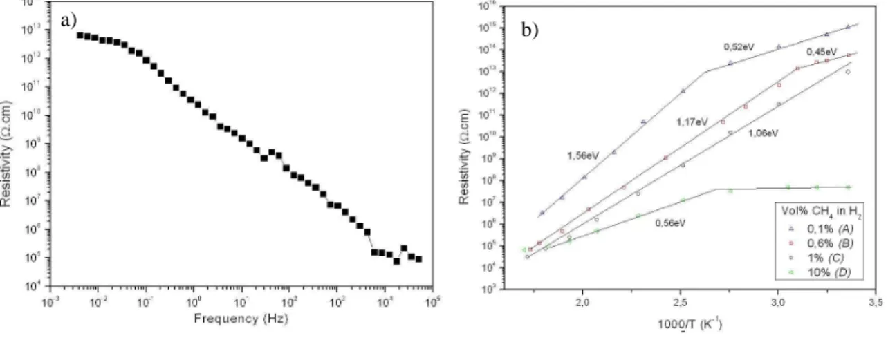
It is well known that the resistivity of diamond decrease strongly with the frequency of the applied AC field [10]. In Fig. 1a, we observe that the resistivity of CND (sample B) strongly decreases from static field to high frequency (8 orders of magnitude). To prevent this current leakage through the diamond bulk in SOD application, we need to understand the conduction mechanisms which take place into such diamond films. As the samples were synthesized with different fractions of methane, we could access to materials presenting the same grain size but different chemical quality and morphology.
SEM micrographs, displayed in Fig. 2, show the morphology of the 4 samples. We observed that the crystal quality, in terms of secondary nucleation, changes with the fraction of methane. The samples grown with the lower methane concentration exhibit crystal faces without secondary nucleation (samples A and B). Sample D (10% CH4) could not be considered as a columnar nanostructured material because the secondary nucleation is
too important for columnar growth [13].
Fig. 1b shows the evolution of the diamond layers resistivity with respect to the inverse of the temperature. The logarithm of the resistivity allows extracting the slop of the curve and thus measured the activation energy of the different defects present in the diamond films. The static resistivity (σs) of the CND, respectively A and B,
decreases from 1015 to 1013 Ω.cm when the methane concentration increases. Sample D exhibits a static resistivity of 5×10⁷ Ω.cm, far underneath the columnar nanostructured material. The samples with the lower methane concentration (A, B) exhibit clearly two different defects conduction mechanisms. The electrical conductivity
σ
is described by equation (1), with σs the static conductivity, σ1 the conductivity due to shallowerdefects (<0.52 eV) and σ2, the conductivity due to deeper defects (>0.52 eV) and T, the temperature.
(1)
σ
=
σ
s+
σ
1(
T
)
+
σ
2(
T
)
The shallower activation energies (<0.52eV) are in this study considered to be responsible for the hopping transport leading to the detrimental leakage current at room temperature described in Fig. 1a. We observe that
the hopping conduction could be described by NNH (Nearest Neighbour Hopping) as well as VRH (Variable Range Hopping) [14].
From Fig. 1b, we also observe that the defects activation energy decrease with the increasing of secondary nucleation on the sample crystal faces. Indeed, sample A (0.1% CH4) exhibits crystal faces with few secondary
nucleations and possess the best electrical feature with defects activation energies of 0.52 and 1.56 eV. It is also important to notice that the temperature influence is weaker on diamond with enhanced crystal morphology.
EHT=20kV WD=3mm InLens 10% CH4 (D) 400nm EHT=20kV WD=3mm InLens 1% CH4 (C) 400nm EHT=20kV WD=3mm InLens 0.1% CH4 (A) 400nm EHT=20kV WD=3mm InLens 0.6% CH4 (B) 400nm
FIGURE 2. SEM micrographs of samples A, B, C and D. The thickness of the samples is 350±30nm. FIGURE 1. Evolution of the diamond layer electrical properties. Fig 1a) Evolution of the diamond layer resistivity
with respect to the frequency of the applied electrical field. The sample was grown in condition comparable to sample B. Fig 1b) Electrical resistivity compare to the inverse of the temperature for the four different samples.
b) a)
CONCLUSION
Polycrystalline diamond films were synthesized with different morphology due to the different fraction of methane applied during the growth step. We observe that the dielectrical resistivity of these films decreases drastically with the increasing of the electrical field frequency. For the samples exhibiting a columnar nanostructure (sample A and B), hopping conduction through shallow traps (<0.52 eV) was found to be responsible for the electrical resistivity drop. Diminishing the fraction of methane during the growth diminish the secondary nucleation on the diamond crystal faces and increases the defects activation energy. The best electrical resistivity was found for low methane synthesis (0.1% CH4) and leads to columnar nanostructured diamond
layers with reduced secondary nucleation. The static resistivity of such diamond film is 1015 Ω.cm. We also observed that the resistivity decreases more slowly with the temperature for sample A.
ACKNOWLEDGMENTS
We acknowledge the ANR for the funding of the DIATHERM (ANR-05-NANO-057) and CARNOT projects aiming at diamond layer optimization for SOD applications.
REFERENCES
1. J. P. Mazellier, O. Faynot, S. Cristoloveanu, S. Deleonibus, P. Bergonzo, Diamond and Related Materials 17, 1248 (2008). 2. J.P. Mazellier, J. Widiez, F. Andrieu, M. Lions, S. Saada et al., SOI Conference IEEE International, p.1-2, (2009). 3. A. Aleksov, J. M. Gobien, X. Li, J. T. Prater, Z. Sitar, Diamond and Related Materials 15, 248 (2006).
4. Y. V. Pleskov, M. D. Krotova, V. G. Ralchenko, A. V. Khomich, R. A. Khmelnitskiy, Electrochimica Acta 49, 41 (2003). 5. J. C. Madaleno, S. C. Trippe, L. Pereira, Diamond and Related Materials 16, 926 (2007).
6. C. Jany, A. Tardieu, A. Gicquel, P. Bergonzo, F. Foulon, Diamond and Related Materials 9, 1086 (2000). 7. M. Lions, S. Saada, J.-P. Mazellier, F. Andrieu, O. Faynot, P. Bergonzo, Physica Status Solidi RRL 1–3 (2009).
8. M. Lions, S. Saada, B. Bazin, M.-A. Pinault, F. Jomard, F. Andrieu, et al., Diamond and Related Materials 19, 413 (2010)
9. H. T. Ye, R. B. Jackman, and P. Hing, Journal of Applied Physics 94, 7878 (2003).
10. T. Sugino, Y. Muto, K. Karasutani, J.Shirafuji, Diamond and Related Materials 2, 803 (1993). 11. B. Fiegl, R. Kuhnert, M. Benchorin, F.Koch, Applied Physics Letters 65, 371 (1994).
12. S. Saada, J. C. Arnault, L. Rocha, B.Bazin, P.Bergonzo., Physica Status Solidi A 205, 2121 (2008).
13. O. A. Williams, M. Nesladek, M. Daenen, S.Michaelson, et al., Diamond and Related Materials 17, 1080 (2008). 14 E Trajkov