HAL Id: tel-01743712
https://tel.archives-ouvertes.fr/tel-01743712
Submitted on 26 Mar 2018HAL is a multi-disciplinary open access archive for the deposit and dissemination of sci-entific research documents, whether they are pub-lished or not. The documents may come from teaching and research institutions in France or abroad, or from public or private research centers.
L’archive ouverte pluridisciplinaire HAL, est destinée au dépôt et à la diffusion de documents scientifiques de niveau recherche, publiés ou non, émanant des établissements d’enseignement et de recherche français ou étrangers, des laboratoires publics ou privés.
Modelling, characterisation and optimization of
substrate losses in RF switch IC design for WLAN
applications
Fadoua Gacim
To cite this version:
Fadoua Gacim. Modelling, characterisation and optimization of substrate losses in RF switch IC design for WLAN applications. Electromagnetism. Normandie Université, 2017. English. �NNT : 2017NORMC268�. �tel-01743712�
1 THESE
Pour obtenir le diplôme de doctorat
Spécialité Electronique, Microélectronique, Optique et Lasers, Optoélectroniques, Microondes
Préparée au sein de l’ENSICAEN et de l’UNICAEN
Modelling, Characterisation and optimization of substrate losses
in RF switch IC design for WLAN application
Présentée et soutenue
par
Fadoua GACIM
Thèse dirigée par Philippe DESCAMPS et Olivier TESSON, laboratoire CRISMAT
Invités :
Mme Nathalie JOURDAN : Ingénieur PDK, NXP Semiconductors, Caen
Mr Hans van WALDERVEEN : Senior Scientist, NXP Semiconductors, Eindhoven, Pays Bas
Thèse soutenue publiquement le (19 Décembre 2017) devant le jury composé de
Mr Patrice GAMAND Ingénieur HDR, université de Limoges Examinateur
Mr Jean-Baptiste BEGUERET Professeur des universités, Bordeaux Rapporteur
Mr Emeric De FOUCAULT Chercheur HDR, Université de Grenoble Rapporteur
Mr Domine LEENAERTS Professeur, Technische Universiteit, Eindhoven, Pays Bas
Examinateur
Mr Philippe DESCAMPS Professeur des universités, ENSICAEN Directeur de thèse
Mr Olivier TESSON Ingénieur HDR, NXP Semiconductors,
2
Acknowledgements
During my PhD work I met wonderful people who gave real fundamental contributions to my personal and professional growth. I do not know if I will be able to really thank all of them.
This CIFRE thesis was realized through a collaboration between NXP Semiconductors-Caen and the University of Caen Normandy.
First of all, my special and deep appreciation is for my advisor at NXP, Dr-HDR Olivier Tesson. For his continuous support of my PhD study and related research. For his patience, motivation, and immense knowledge. For all the time of research reviewing this thesis and almost all the papers I published, I owe him immense gratitude.
Beside my supervisor I would like to thank my co-advisor at NXP, Mrs. Nathalie Jourdan for advices she gave me with her always optimistic attitude, always believing in my abilities. Many thanks to Prof. Philippe Descamps, my supervisor from the University of Caen Normandy, for the many advices and recommendations he gave me. And also his administrative efforts to ensure that the defense took place in a satisfactory manner.
I would like to thank Prof. Jean-Baptiste Begueret and Dr-HDR Emeric de Foucault who have kindly reported this thesis and gave their favorable opinion so that I can defend my work and obtain the title of Doctor of the University of Caen. I also thank all the members of my jury who agreed to give some of their time to take an interest in my work. Dr-HDR Patrice Gamand, Prof. dr. ir. Domine Leenaerts and Hans van Walderveen for their valuable comments, recommendations and careful review of my manuscript.
I would to express my deep gratitude to Mrs. Dominique Lohy manager of the PDK team in NXP-Caen, who was able to make this CIFRE thesis possible in a cross collaboration between the PDK team and the design team (BL-SAS). She made me feel very welcome in the team and has been a source of love and energy ever since.
Special thanks for the people who helped me technically. A big thank to Hans van Walderveen from NXP-Eindhoven, Dr.ir. Peter Magnée from NXP-Nijmegen, Dr. Cristian Andrei from NXP-Caen, Sylvie Parmantier from Cadence, Dr-HDR Sidina Wane and of course Dr-HDR Olivier Tesson from SAS-Caen. Many thanks to Dominique Lesenechal for his help to make all my measurements possible. I would like to also thank Samuel Mabire and Olivier Minchin for helping me in ‘tool-fighting’. Mrs. Carole Aubey and Melina for their efficiency and kindness, many things could not have been done without their interventions. I also would like to thank Cees van Dinther and ir Michel Groenewegen for having received me in the SAS team at NXP-Nijmegen. Many thanks to ir Michel Groenewegen who took the time and made a special trip to be present at my thesis defense.
In my daily work I have been blessed with a friendly and cheerful group, Dominique Lohy, Nathalie Jourdan, Didier Leroux, Jean-Francois Aupee, Sylvie-anne Leverd, Jean-Yves Queignec, Christophe Lecoutre, Didier Depreeuw, Hubert Furdyna, Christele Biard and Emmanuel Grenados. Thank you for all your support and good cheers! I love you all and I could not express in a few lines my gratitude for you.
Thanks to my supervisor of my final year internship Manohiana Ranaivoniarivo who provided me an opportunity to join her team as intern at NXP Semiconductors.
I finish with the most basic source of my life energy: my family, my parents: mom Hasna Hammouka and dad Jilali GACIM. My brother Salah-Eddine, my sister Safaa and my little nephew Adam. I have an amazing family; their support has been unconditional all these years; they have given up many things for me; they have cherished with me every great moment and supported me whenever I needed it. And I want to thank them now: MERCI!!!
3
Table of contents
ACKNOWLEDGEMENTS ... 2
TABLE OF CONTENTS ... 3
GENERAL INTRODUCTION ... 5
CHAPTER I:CONTEXT AND STATE OF THE ART OF MODELLING TECHNIQUES FOR RFIC’S ... 8
INTRODUCTION ... 9
I.1. TYPES OF PARASITIC COUPLING IN INTEGRATED CIRCUITS ... 10
I.1.1. Crosstalk effects in integrated circuits ... 10
I.1.2. Passive elements and metal losses ... 11
I.1.3. Substrate effects in integrated circuits: ... 14
I.2. CIRCUIT PARASITIC MODELLING ... 18
I.2.1. RLCk extraction method ... 18
I.2.2. Compact model ... 19
I.2.3. Macro-modelling based techniques ... 19
I.2.4. Finite Element Method -FEM ... 20
I.2.5. Finite Differences Method in Time Domain-FDTD ... 21
I.2.6. Method of Moments-MoM ... 22
I.3. SUBSTRATE NETWORK ANALYSIS METHODOLOGY ... 25
I.3.1. Substrate network analysis integration in NXP’s design flow ... 25
I.3.2. Substrate extraction ... 27
I.3.3. Align device model and substrate extraction ... 28
I.4. FRONT-END RFIC DESIGN AND GENERAL CONSIDERATION ... 29
I.4.1. Receiver architecture ... 29
I.4.2. Design Considerations ... 30
I.5. CONTEXT AND CHALLENGES BROUGHT OUT ... 33
I.5.1. Motivation ... 33
I.5.2. The proposed methodology to account for substrate effects ... 33
I.5.3. The challenges ... 34
I.6. SYNTHESIS AND CONCLUDING REMARKS: NECESSITY OF DEVELOPING A METHODOLOGY FOR MODELLING RF SWITCHES ... 35
REFERENCES OF CHAPTER I ... 36
CHAPTER II:EVALUATION, CHARACTERIZATION, MODELLING AND ANALYSIS OF SINGLE ISOLATION STRUCTURES ... 40
INTRODUCTION ... 41
II.1. TECHNOLOGY DESCRIPTION ... 42
II.1.1. BiCMOS process description ... 42
II.1.2. Deep Trench Isolation-DTI in BiCMOS technology ... 44
II.2. MAIN SUBSTRATE ISOLATION TECHNIQUES ... 47
II.2.1. Guard Ring ... 47
II.2.2. Buried layers ... 48
II.2.3. Pwell block and Buried P block layers ... 48
II.2.4. Deep-Trench-Isolation ... 48
II.3. SUBSTRATE ISOLATION INFLUENCE ON PASSIVE ELEMENTS ... 50
II.4.1 The influence of Deep Trench Isolation on coils ... 50
II.4.2 Modelling of inductors in circuit simulation ... 51
II.4. SUBSTRATE EXTRACTION BETWEEN TWO SUBSTRATE TAPS ... 57
II.4.1. Substrate taps ... 57
II.4.2. Substrate network extraction & analysis ... 57
II.4.3. Substrate network extraction without DTI ... 58
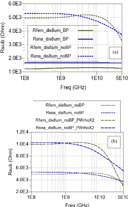
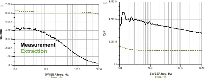
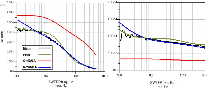
II.4.4. Increasing the substrate impedance between ports ... 61
CONCLUSIONS ... 66
REFERENCES OF CHAPTER II ... 67
CHAPTERIII:APPLYING ISOLATION AND MODELLING RELATED TECHNIQUES TO NMOS SWITCH DEVICE ... 69
INTRODUCTION ... 70
III.1. THE NMOS SWITCH DEVICE ... 71
III.1.1. Substrate body tuning technique in BiCMOS switches... 73
III.1.2. Test case descriptions ... 75
4
III.1.3. RF measurements setup ... 75
III.1.4. RF measurements results and Discussions ... 76
III.1.5. FEM modelling to account for substrate effect ... 77
III.1.6. Measurement/simulation correlations ... 80
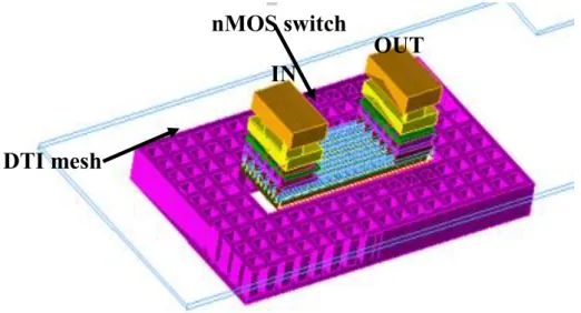
III.2. DTI EFFECT ON NMOS SWITCH PERFORMANCES ... 83
III.2.1. Design description... 83
III.2.2. Measured Results for the nMOS Devices ... 85
III.2.3. Modelling technique and comparison with measurements ... 89
III.3. SUBSTRATE ISOLATION’S RECOMMENDATIONS USING DTI ... 92
CONCLUSIONS ... 94
REFERENCES OF CHAPTER III ... 95
CHAPTER IV:MODELLING METHODOLOGY FOR PREDICTIVE ANALYSIS OF SUBSTRATE EFFECTS IN AN RFSWITCH ... 96
INTRODUCTION ... 97
IV.1. LTESPXT SWITCH ... 98
IV.1.1. SPDT test cases description ... 98
IV.1.2. RF Measurement set-up of SPDT and SP8T ... 101
IV.1.3. SPDT Measurement Results ... 102
IV.1.4. SPDT modelling methodology and comparison with measurements ... 103
IV.2. SP8T DESIGN DESCRIPTION ... 110
IV.2.1. SP8T modelling methodology ... 111
IV.2.2. Comparison of switch performances in various technologies ... 116
CONCLUSIONS ... 119
REFERENCES OF CHAPTER IV ... 120
CHAPTER V:MODELLING METHODOLOGY FOR A PREDICTIVE ANALYSIS OF SUBSTRATE EFFECTS IN RFIC DESIGN ... 121
INTRODUCTION ... 122
V.1. RF SWITCH ARCHITECTURES AND SPECIFICATIONS ... 123
V.1.1. Design description... 123
V.1.2. Design methodology ... 124
V.1.3. Test Case Descriptions ... 135
V.1.4. Modelling Methodology ... 140
V.1.5. Correlation with FEM Analysis and Measurements ... 143
CONCLUSIONS ... 149
REFERENCES OF CHAPTER V ... 150
GENERAL CONCLUSIONS ... 152
PERSPECTIVES ... 154
5
General Introduction
The evolution and the development of high performance wireless communication systems like the cellular system, Bluetooth, the wireless local area network (WLAN), etc., involve ever-increasing complex Radio Frequency Integrated Circuits (RFICs) to support this growth.
The wireless revolution where different devices are connected simultaneously makes it possible to communicate anywhere at any time. Recent developments in wireless networking using different standards exhibit several challenges. The most critical challenges are: Low cost/Low power/High integration in a small form factor for RF functions and Multi-mode/Multi-band operations. In addition, the decreased feature size of the integration technologies leads to higher complexity as it is required for highly integrated transceivers for mobile communication and wireless networking. This requires choosing an optimized technology as well as the development of new design strategies.
Figure I. 1.IC application's road map
For high-frequency and high-power integrated solutions, a good choice of semiconductor substrate technology can provide a strategic advantage by achieving better performance without additional design cost. A material such as gallium arsenide (GaAs) has traditionally been the substrate of choice for RF applications [I-12]. However, the large scale of commercial RF applications requires a substrate that is low cost, like silicon, and also present low losses.
Due to the high operating speed of state-of-the art bipolar transistors, combined with high-density CMOS in BiCMOS technologies (for example BiCMOS- from NXP), it becomes possible to realize integrated circuits for very challenging applications.
RF circuit designs have tight requirements on power consumption and noise figure (NF). The accuracy of circuit simulation and its related predictability is very crucial in meeting those
6 requirements. This is highly linked to the accuracy of the models with their intrinsic and extrinsic effects. Therefore, for successful design of such circuits, it is mandatory to consider accurately parasitic effects, including the influence of the substrate, as early as possible during circuit design to reduce the number of design iterations and thus reduce ‘time to market’.
The substrate impedance is therefore an important extrinsic element in the performance of the circuits. It then needs to be accurately modelled for predictable simulations.
This thesis deals with substrate characterization and optimization in RFIC’s, and the development of an efficient methodology for parasitic extraction of inhomogeneous substrates, offering a challenging trade-off between required accuracy and fast simulation.
The interest in developing a substrate extraction technique is twofold. First, it will allow a deeper physical understanding of the different coupling mechanisms in the silicon substrate. Secondly, in addition to the development of reduction techniques of the substrate effect, it is important to define simple and fast simulation methods to handle the substrate coupling effects in complex circuits.
This manuscript consits of the following chapters:
Chapter 1 presents the context and state of the art of coupling effects in Integrated Circuits, to define clearly the circuit environment, and to initiate discussions on the root cause of the mismatch between measurements and simulation. This is key to identify the areas that should be explored in more detail. The purpose of chapter 1 is to give a global background of modelling techniques and the position of this thesis in that context.
Chapter 2 presents the predictable substrate modelling technique that has been developed in this PhD program. The accuracy and sensitivity of the proposed methodology have been verified on a single test case with different layout variants of Deep Trench Isolation. From measurements analysis, we will be able to get more knowledge about isolation strategy (especially in relation to DTI).
Chapter 3 focuses on the role of substrate isolation techniques on nMOS switch performances, Design recommendations on isolation techniques (from a layout point of view) at device level are also presented in this chapter. The proposed method has been validated using measurement results and EM simulations (both 2.5D and 3D FEM) for accuracy and flow usability.
Chapter 4 will propose the ad-hoc approach one step further considering a full IP (SP2T and SP8T circuits) This IP has been developed in-house using an NXP BiCMOS technology. RF measurements are presented to support theoretical investigations. A comparison between simulations and experimental data is also presented and discussed in view of the criteria accuracy and development-time.
Chapter 5 demonstrates how to use the proposed methodology in the development of a full SP3T switch embedded in a commercial product for WLAN related applications. This switch will be described in detail in this chapter. It includes the series and parallel switches but also the ESD protection (which are known to couple with the substrate and thus leading to additional losses). A bias block together with a decoder are also included in this topology. In this chapter, challenges
7 related to database partitioning will be presented. We will highlight the way we have succeeded to solve these issues by adopting a new methodology. Results are then compared to both measurements and the prior methodology.
Finally, we will draw some conclusions inherent to the methodology itself and the way we can also minimize losses related to substrate coupling. Layout recommendations will be provided based on the available data.
8
Chapter I: Context and state of the art of modelling techniques for
RFIC’s
INTRODUCTION ... 9
I.1. TYPES OF PARASITIC COUPLING IN INTEGRATED CIRCUITS ... 10
I.1.1. Crosstalk effects in integrated circuits ... 10
I.1.2. Passive elements and metal losses ... 11
I.1.3. Substrate effects in integrated circuits: ... 14
I.2. CIRCUIT PARASITIC MODELLING ... 18
I.2.1. RLCk extraction method ... 18
I.2.2. Compact model ... 19
I.2.3. Macro-modelling based techniques ... 19
I.2.4. Finite Element Method -FEM ... 20
I.2.5. Finite Differences Method in Time Domain-FDTD ... 21
I.2.6. Method of Moments-MoM ... 22
I.3. SUBSTRATE NETWORK ANALYSIS METHODOLOGY ... 25
I.3.1. Substrate network analysis integration in NXP’s design flow ... 25
I.3.2. Substrate extraction ... 27
I.3.3. Align device model and substrate extraction... 28
I.4. FRONT-END RFIC DESIGN AND GENERAL CONSIDERATION ... 29
I.4.1. Receiver architecture ... 29
I.4.2. Design Considerations ... 30
I.5. CONTEXT AND CHALLENGES BROUGHT OUT ... 33
I.5.1. Motivation ... 33
I.5.2. The proposed methodology to account for substrate effects ... 33
I.5.3. The challenges ... 34
I.6. SYNTHESIS AND CONCLUDING REMARKS: NECESSITY OF DEVELOPING A METHODOLOGY FOR MODELLING RF SWITCHES ... 35
9
Introduction
Chapter I presents the motivation and the objective of the thesis. This chapter is organized as follows: The first section describes the main parasitic effects in Integrated Circuits. The physical behaviour of the silicon and the contribution of the substrate losses are highlighted. In the second section, we discuss the modelling techniques with the advantages and limitations of each approach. The third section presents the predictive methodology proposed in this thesis. The mechanism and the implementation in NXP of this methodology in the design flow are described. The fourth section presents the design consideration in Front End Integrated Circuits. Then we will discuss the thesis motivation and the challenges to meet. Finally, the last paragraph concludes this chapter.
10
I.1. Types of parasitic coupling in Integrated Circuits
In the introduction of this book it is shown how trends towards greater complexity, increasing performance and reducing size makes the timely prediction of coupling mechanisms more and more important. In-circuit disturbances, can limit the circuit performance, so they should be considered in all stages of the design process. The main mechanisms of electric coupling in IC’s are presented in the following paragraph. More generally, there are thousands of couplings in IC’s, but most of them compensate each other. In the following parts of this section we will discuss main coupling contributors and the way they can be anticipated at design phase (extraction).
I.1.1. Crosstalk effects in integrated circuits
Crosstalk can be defined, as an unwanted interference caused by the electric and magnetic fields of one circuit (aggressor) affecting another one (victim) [I-23]. From this general definition, it can be deduced that any mechanism that creates such type of interference falls into the crosstalk definition. In the case of high-frequency ICs, coupling through the substrate – the so-called substrate crosstalk – is one of the main sources of interference. It is recognized as one of the most limiting factors in the performance of RF ICs [I-16] [I-17]. Many techniques have been developed to reduce this loss of performance, one of the possibility is to use a (so-called) less lossy substrate like: GaAs, Silicon-On-Isolator (SOI), Silicon-On-Sapphire (SOS), high-resistive silicon (HRS), Glass, quartz, or to etch the substrate away under the device (macro mechanical system - MEMS) [I-49]. But the mechanical stability, process ability and packaging of such structures should be taken in consideration.
Better electrical characteristics than using normal Si substrate can be achieved by applying glass or quartz substrates, but one of the major difficulties is the low thermal conductivity of these materials that may severely limit the maximum dissipated power of the package. SOS combines several of the benefits in term of cross talk reduction and thermal conductivity, but it has a poor mechanical stability, which, is excellent for bulk silicon [I-50].
To address these issues more favourably, other materials that have a higher thermal conductivity and allow for high-density through-wafer interconnects should be considered. High-resistive silicon meets most of these requirements.
Crosstalk in silicon substrates is caused by three different mechanisms: injection into the substrate, the propagation of the noise signal through the substrate and the sensitivity of an adjacent circuit to pick up this noise signal. Various isolation strategies which are layout dependent have been made to reduce crosstalk. In general, crosstalk reduction strategies fall into two different categories: One is to attempt to block crosstalk signals and the other is to drain the crosstalk signal to ground.
Crosstalk is expressed in dB as follows:
𝐶𝑟𝑜𝑠𝑠𝑡𝑎𝑙𝑘 (𝑑𝐵) = 20 log(
𝑐𝑜𝑢𝑝𝑙𝑒𝑑 𝑣𝑜𝑙𝑡𝑎𝑔𝑒 𝑎𝑡 𝑟𝑒𝑐𝑒𝑖𝑣𝑒𝑟𝑠𝑖𝑔𝑛𝑎𝑙 𝑣𝑜𝑙𝑡𝑎𝑔𝑒 𝑖𝑛 𝑠𝑜𝑢𝑟𝑐𝑒
)
(I-1)In integrated circuits, there are generally: electric field coupling, magnetic field coupling and substrate coupling.
11 Electric field coupling:
This kind of coupling occurs when electric field lines originate from one conductor and terminate to another. This can be represented schematically by a parasitic capacitance between two conductors. This capacitive coupling (or electric field coupling) between interconnect (isolated by oxide), has been studied in [I-18], [I-10]. The electric field coupling induces a current in the victim conductor (or circuit) that is proportional to the time derivative of the source signal (𝑖 = 𝐶. 𝑑𝑉 𝑑𝑡)⁄ . The larger the capacitance the larger the coupling, which means it increases for closer, longer interconnects and increases with frequency.
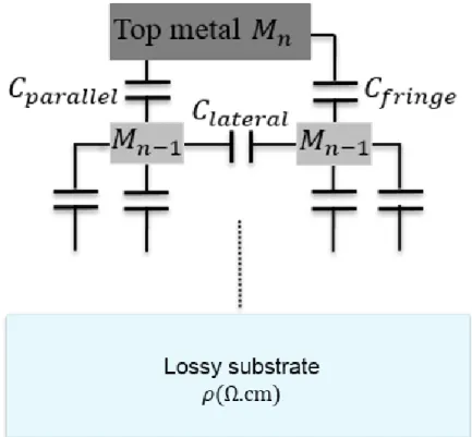
In modern technologies the lateral (intra-layer) dimensions are smaller than the vertical (inter-layer) dimensions. Therefor the lateral capacitances are dominant over the vertical capacitances (Figure I.2).
Figure I. 2.Capacitive coupling between wires in a multi-layered interconnect system
Magnetic field coupling:
Magnetic field coupling or inductive coupling can also be a significant source of crosstalk in Integrated Circuits.
A magnetic field induces a current and its variation generates a voltage in the victim device (or circuit) that is proportional to the derivative of the signal current in the source device (or circuit) [I-18] (𝑉 = 𝐿. 𝑑𝑖 𝑑𝑡⁄ )
I.1.2. Passive elements and metal losses
Passive elements include resistors, capacitors and inductors. In BiCMOS technology, resistors and most capacitors are library components and the available modelling is accurate. When
12 frequency is increasing, modelling is of particular importance as series resistance and inductance can jeopardize capacitor performance. This requires a proper extraction strategy. Inductors are critical components that need to be accurately modelled and optimized for their particular purpose in the design. The right trade-off between Q-factor and chip area is crucial for chip performance and having the smallest area. When current flows through a spiral, a magnetic field that penetrates the substrate induces eddy currents which flow in the opposite direction (Lenz’ Law). This results in a severe loss of the quality factor (Q) of the inductor. If the substrate is sufficiently resistive (∼Ohm•cm), this type of loss is small.
The substrate loss consists of two parts: finite resistance due to electrically induced conductive and displacement currents, and magnetically induced eddy current resistance. These losses are known as capacitive and magnetic, respectively.
One of the difficulties in designing integrated RF circuits is the low Q-factor of on-chip inductors and transmission lines. This is mainly due to the mentioned eddy current in the substrate and the DC resistance of the inductor wires.
Figure I. 3.Integrated coil related losses
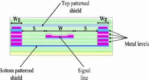
To reduce electromagnetic (EM) couplings and to improve the Q-factor of on-chip inductors, different strategies in [I-6] are applied. These strategies are all targeted at improving the inductor’s intrinsic resistance (by using a thick metal layer or stacked inductors...), modifying its architecture, optimizing the substrate stack (removing low-Ohmic buried layers, using Deep Trench Isolation [I-22]), or using a metal shield to decrease the vertical electric field penetrating into the substrate. These include metal ground shield (MGS), polysilicon ground shield (PGS) and n+ ground shield (NGS) [I-39]. Solid ground shields result in a very large capacitance between the trace and the
13 ground plane, in a lower inductance and SRF (self-resonance frequency). Therefore, a patterned shield (Figure I.4) provides isolation from the substrate and thus no eddy currents will be induced in the substrate, which leads to an improvement of the Q-factor. However, that can reduce the SRF.
Figure I. 4.Electrical field suppression using MGS or PGS
Another technique is based on the use of a Via-hole connection and a Faraday cage (Figure I.5) to shield it from high frequency paths[I-51].
Figure I. 5.Cross section representation of 1line configuration embedded in a metal cage
This technique offers a higher density of integration and allows proper grounding connection leading to a higher flexibility of routing. Although this technique is applicable to SiP application using TSV (Through Silicon Via). However, it can include spurious resonant modes, and requires properly designed grounding strategies to avoid floating configurations.
14 I.1.3. Substrate effects in integrated circuits:
Substrate coupling in IC’s is the process whereby a parasitic current flow in the substrate creates an electrical coupling between devices and/or circuits due to the presence of conductive and capacitive paths in the silicon substrate.
Current is injected into the substrate through various mechanisms. Physically large passive devices such as inductors, capacitors, interconnect and bond-pads inject displacement current in the substrate. These currents flow vertically and horizontally to points of low potential in the substrate, such as substrate taps and the back-plane. These currents couple to other large passive structures in a similar manner [I-19].
Active devices also inject current into the substrate. For this reason, a lot of effort has been put into isolating active devices from the substrate by either reverse-biased PN junctions, Faraday cage, SOI or other isolation techniques [I-40] [I-41] [I-42] [I-43].
The current can also be injected into the substrate by means of the hot electron effect. In a short-channel MOS transistor, for instance. There the electron-hole pair mechanism takes place in the high-field pinch-off region near the drain due to collisions. The electric field lines lead one set of the carriers into the substrate.
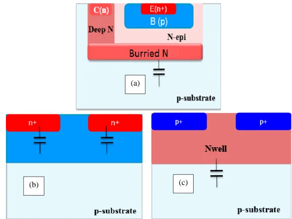
Another mechanism, by which parasitic currents can be injected into the substrate, is capacitive coupling. This can be caused by the interaction of bipolar NPN transistors and the substrate through the N-type collector (BN) to the n/p-substrate junction. This capacitive coupling can also be caused by a MOS transistor through the source-substrate and drain-substrate junction capacitances. Figure 1.6 summarizes the capacitive coupling mechanisms.
Figure I. 6Capacitive coupling to the substrate through PN junction: (a) in NPN transistor (b) in nMOS transistor, (c) in pMOS transistor
(b) (c)
15 Those capacitances give a path for the current to propagate into the substrate. Its values depend on the doping profile levels as well as the bias level.
Furthermore, in an integrated circuit, the coupling between different portions of the chip can be very problematic. Although careful layout techniques and isolation strategies can minimize them, these effects can never be eliminated or ignored in ICs. Substrate coupling is treated extensively in [I-23].
Figure I. 7 Parasitic effect to be considered during design simulation
The substrate is a major source of loss and limitation of high-frequency signals, which is a direct consequence of the conductive nature of Si as opposed to the insulating nature of GaAs. The Si substrate resistivity varies from some kΩ.cm for lightly doped Si to few mΩ.cm for heavily doped Si.
The Si-substrate influences the behaviour of the integrated circuit design in a negative manner. The capacitance between interconnect (wires) and the substrate delays the signal through the interconnection. The current flowing to ground through the substrate causes a voltage drop, which affects the device operation in a negative manner. In addition, the substrate is not a perfect isolation between devices, leading to unwanted “cross-talk” through the substrate. Figure 1.7 illustrates coupling phenomena to be considered in addition.
In fact, to tackle these substrates induced losses, some papers [I-56] already propose different isolation techniques.
In this thesis, we develop a predictable modelling methodology which can handle accurately the considered isolation technique by the designer and thus help on the minimization of the substrate related losses.
Substrate physical equivalent model:
It is essential to know how the signal propagates from one device to anther or from one circuit to another. Therefore, it is necessary to understand the mechanism and the physics of the substrate to be able to model accurately the substrate.
16 𝑗⃗ = (𝜎 + 𝑗𝜔ɛ)𝐸⃗⃗ (I-2)
where j is the current density in the substrate (A/𝑐𝑚2 ), σ the conductivity, ε the dielectric
permittivity of the silicon, 𝜔 the angular frequency and 𝐸⃗⃗ the electric field strength (V/cm). Ohm’s law consists of a real part and an imaginary part, describing the conductive behaviour and capacitive behaviour, respectively.
Particular case regarding Silicon
Silicon, as any semiconductor material, exhibits both conductive and dielectric characteristics, which can be translated into a resistive and a capacitive effect, respectively.
Inside a doped semiconductor, the conductivity is given by: 𝜎 = 𝑞( µ𝑝 𝑝 + µ𝑛 𝑛) (I-3)
Where q is the electron charge, µ𝑛 and µ𝑝 represent the mobility of the electrons and holes carriers, and n and p stand for the respective carrier densities. The µ𝑛 and µ𝑝 parameters vary as function of the total semiconductor doping and temperature.
At low frequencies, silicon can be considered as ohmic for signal below of the frequency 𝑓𝑐 and
the associated capacitive effect can be neglected. As the frequency increases, the capacitive effect rises to become equal to the resistive effect at the cut-off frequency defined by[I-36]:
1
𝑅𝑠
= 𝜔
𝑐𝐶𝑠 = 2𝜋𝑓
𝑐𝐶𝑠 ; 𝑓
𝑐=
𝑞( µ𝑝 𝑝+ µ𝑛 𝑛)
2𝜋ℰ0ℰ𝑟𝑠𝑖 (I-4)
Resistive effect:
The substrate can be modelled as mainly resistive for frequencies from DC up to a cut-off frequency [I-36], which is defined as:
𝑓
𝑐=
12𝜋 𝜌𝑠𝑢𝑏 ɛ𝑠𝑢𝑏 (I-5)
Where 𝝆𝒔𝒖𝒃 and ɛ𝒔𝒖𝒃 are the resistivity and the permittivity of silicon, respectively.
In the case of the BiCMOS technology that is used to support this study, the resistivity of the substrate is 200 Ωcm. According to (I-5), the behaviour of the substrate is mainly resistive for frequencies up to 760 MHz.
Capacitive effect:
At frequencies above the cut-off frequency, the dielectric behaviour of the semiconductor can no longer be neglected, thus the substrate must be modelled as an RC (resistive and capacitive) network as shown in Figure I.8.
17
Figure I. 8.RC model of a piece of substrate
Figure I.9 represents the lumped element equivalent circuit used to describe the crosstalk effects between two devices in silicon substrate. The two capacitors and resistors 𝐶𝑠𝑖, 𝑅𝑠𝑖 represent the coupling effect between the bottom of each device and the back-side of the wafer [I-34] [I-35]. These capacitors and resistors are defined by:
𝑅𝑠𝑖 = 𝑡𝑠𝑖
𝜎𝑠𝑖𝐴𝑑𝑒𝑣𝑖𝑐𝑒 (Ω) , 𝐶𝑠𝑖=
ℰ0ℰ𝑟𝑠𝑖𝐴𝑑𝑒𝑣𝑖𝑐𝑒
𝑡𝑠𝑖 (I-6)
With ℰ𝑟𝑠𝑖and 𝑡𝑠𝑖 being the permittivity and the thickness of the silicon, respectively, and 𝐴𝑑𝑒𝑣𝑖𝑐𝑒 the area considered at terminals 1 and 2.
Figure I. 9.Lumped equivalent R-C model substrate crosstalk in the case of BiCMOS substrate
When two devices are close enough, a portion of the signal present at one device is transferred to the second device by coupling. This coupling effect is modelled by the parameters 𝑅𝑐𝑜𝑢𝑝𝑙𝑒 and 𝐶𝑐𝑜𝑢𝑝𝑙𝑒.
18
I.2. Circuit parasitic modelling
Parasitic effects are becoming more critical with increasing requirements on performance, density, complexity, and levels of integration in RFIC designs. For radio frequency (RF) designs, parasitic effects such as IC package pin leakage and substrate coupling are now widely seen. This leads to the need to model the parasitic networks in the areas of chip-package and substrate.
This section is organized as follows. A brief survey and the description of the various techniques used in resistance, capacitance and inductance extraction are presented. In terms of solution methods, both the domain methods that solve differential Maxwell equations such as finite difference (FD) [I-26] and finite element (FE) [I-24] methods, as well as integral equation approaches such as method of moments (MoM) [I-28] are discussed. From the accuracy standpoint, two-dimensional (2-D), quasi-3-D (or 2.5-D), 3-D, and quasi-static techniques are covered.
I.2.1. RLCk extraction method
This technique is a quasi-static analysis performed by EDA commercial tools (Assura, Calibre, …) design environments and is based on an approximate segmentation technique to compute quickly the couplings between interconnection of components. It is fast and accurate enough RF applications [I-2].
The tool extracts resistance (R), capacitance (C), self (L) and mutual (k) inductance parameter extractions as shown in figure 1-10.
Figure I. 10.Illustrative multi-line conductors model extraction using PEX
This technique makes it possible to relate the RLCk model (parasitic netlist) with the intrinsic device implicitly, which leads to a simple post-layout simulation for the user. Also, time and frequency domain simulation are both possible. However, the real challenge with this technique is the local ground references and the return path of the inductive currents. All the substrate taps are assumed to be at the same potential. therefore, a near or a far substrate tap will be all shorted to
19 the same (global) ground. This model presents a limitation regarding the substrate behaviour and limits its use at backend interconnect parasitic.
I.2.2. Compact model
In this method, components in design kit libraries are described by lumped element behavioural models, obtained from measurement and characterization for limited geometries and layout topologies. In addition, these models do not include the full substrate model and even if in the future will support the substrate network it will be strongly layout and technology dependent. Therefore, it is not able to give more freedom for designers. However, it is not possible to capture the substrate coupling effect between blocks [I-3]. The most well-known models available on the market are [I-52] [I-53] [I-54] [I-55]:
MOS: PSP, bsim
Bipolar: Mextram, HICUM Passive devices: TLIM, LSIM
I.2.3. Macro-modelling based techniques
In this part, we explore a methodology to extract, from EM simulation results and measurement data, equivalent circuits for passive circuits. This approach is oriented around fitting techniques to find the best matching models representations. Many efforts have been addressed to the macro-modelling approaches to reduce the complexity while maintaining an acceptable accuracy.
Extraction of equivalent Circuits for Passive Circuits (lumped-element model)
An RLCG equivalent circuit is derived from Z or Y-parameters (Figure I.11). Y-parameters are convenient if we want to model our circuit under test with elements in a pi topology (one component across, and two in shunt). Z-parameters are convenient when we want to model the circuit with a T type of topology (two components in series with a shunt element between them) [I-31].
Each branch of the π or T equivalent topology is represented by an admittance or by an impedance, noted in 𝑌𝑝𝑎𝑟𝑎𝑚𝑒𝑡𝑒𝑟𝑠 or 𝑍𝑝𝑎𝑟𝑎𝑚𝑒𝑡𝑒𝑟𝑠 respectively. The series and parallel branches are composed of RLCG.
20
Figure I. 11.PI equivalent topology (a), and T equivalent topology (b)
This model is based on analytical calculations. It represents simply and physically the studied structure. Time domain analysis is also possible. However, it is narrow band and not accurate enough for more complex system. In addition, the difficulty is to find the appropriate equivalent model [I-4].
Black-Box (or S-parameters) model
The Black-Box model contains the measured data or the EM simulated results in S-parameters. This model is frequency dependent. However, this model is only valid in the frequency domain and it presents some limitations in term of causality and time domain analysis. Also, it has some limitations regarding its ability to have predictive simulation.
I.2.4. Finite Element Method -FEM
Resolution by integral equations is only possible if the structure is homogeneous in the resolution area; the later means that ɛ and µ are constant. If ɛ or µ are variable, which corresponds to a non-homogeneous structure we must use a finite element formulation [I-24] [I-25].
The finite elements method (FEM) is widely used in mechanics. It was introduced by P. SILVESTER and MVK CHARI at the beginning of the seventies in the electromagnetic domain to solve non-homogeneous problems and complex geometries. The finite element method is generally applicable in the spectral domain. What is interesting in this method is its inherent capacity to account for non-homogeneous structures.
The first step of the Finite Element Method is to divide the space to be modelled into small elements or pieces of arbitrary shapes, which may be smaller where geometry details require it. In each element, it is assumed that the variation of the field quantity is simple (generally linear). The field is therefore described by a set of linear functions.
21
Figure I. 12.Finite Elements modelling example
Figure.I.12 shows an example of a finite element subdivision. The model contains information about geometry, material constants, excitations and boundary conditions. Each corner of an element is called a node. The goal of the finite element method is to determine the field at each node of the element:
[𝐾]=[𝐹][𝐸]
The global system: [ 𝐾1 ⋮ 𝐾𝑛 ] = [ 𝐹11 ⋯ 𝐹1𝑛 ⋮ ⋱ ⋮ 𝐹𝑛1 ⋯ 𝐹𝑛𝑛 ] [ 𝐸1 ⋮ 𝐸𝑛 ]
Where, E represents the unknown terms at each node which we are looking for, K represents the sources applied on the system. The F-matrix depends on boundary conditions and the geometry studied.
Advantages and disadvantages of the Finite Element Method-FEM
The major advantage of the Finite Element Method over other methods is that in this method each element can have an electrical and geometrical characteristic independent of the other elements. This allows us to solve problems with many small elements in a complex geometry. Thus, it is possible to resolve complex geometrical cases having different properties relatively efficiently. The major disadvantage however of this method is the difficulty of modelling open systems (in the case where the field is unknown at any point of the study domain boundary). One of the big advantages of FEM is also because it includes a mesh algorithm based on refinement.
I.2.5. Finite Differences Method in Time Domain-FDTD
The Finite difference method time domain (FDTD) [I-26] is a computational method using a grid based time domain numerical analysis for solving Maxwell’s equations. The FDTD algorithm was first established by Yee as a three-dimensional solution of Maxwell's curl equations in 1966 [I-27].
The numerical resolution of Maxwell's equations by this method requires a Fine discretization spatio-temporal in squares or cubes with discretization steps 𝛥𝑥, 𝛥𝑦 and 𝛥𝑧. Space is thus divided into elementary parallelepipedal cells, within which the six electromagnetic field components (Ex,
22 Ey, Ez and Hx, Hy, Hz) are calculated. The electric field is solved at a given instant, then the magnetic field is solved at the next instant (in time) and the procedure is repeated several times.
The method makes it possible to solve the Maxwell equations in time and space, by directly approximating the differential operations.
Figure I. 13.The Yee cell
Advantages and disadvantages of the Finite Differences Method in Time Domain-FDTD
The main advantage of this method is that it allows a temporal resolution of the problem and therefore it allows to find the response of a wide frequency band in a single resolution. And its great flexibility to model electromagnetic problems with arbitrary signals propagating in complex configurations of conductors, dielectrics and lossy materials, nonlinear and anisotropic. It also makes it possible to obtain directly the E and H fields.
The major disadvantage however of this method is the compute time and memory requirements. The whole domain to be modelled must be subdivided into cubes and these cubes must be small, relative to the smallest wavelength. These cubes are all the smaller because the geometry is complex. To avoid the problems of dispersion and to obtain a wide frequency spectrum of radiation, it requires very small time steps. In addition, this method calculates only the propagated field; the other parameters such as current distribution are more difficult to calculate.
I.2.6. Method of Moments-MoM
The Method of Moment (MoM) [I-28] is a numerical technique aiming to solve Maxwell’s equations in the frequency domain using their integral form. The electromagnetic field can then be expressed in the form of a surface integral. The decomposition of surface current into basic functions simplifies the resolution of the integral equations, which makes the method simple to implement [I-29] [I-30].
The method of moments (MOM) can be applied either in the spectral domain [I-44]-[I-45], or in the spatial domain [I-46]-[I-47]. The spatial domain approach has the advantage that, in this method, the integrands for the MoM matrix elements need to be evaluated only over the finite extension associated with the basis and testing functions, as opposed to over an infinite range required in its spectral domain counterpart[I-48]. In the conventional form of the spatial domain approach, the closed-form Green’s function is involved.
23 In the case of the open-form Green’s function (spectral domain), all dielectric layers are assumed to have infinite extension in the lateral plane. Therefore, it is not possible to have finite dielectric dimension. The fact that it is limited to homogenous layer stacks, decreases considerably the number of unknowns, and thus makes it possible to tackle complex geometry.
Advantages and disadvantages of the Method of Moments-MoM
The method of moments has the advantage of modelling only the metallic structures and not all the surrounding space. Thus, it is best suited for modelling wires and homogenous structures. However, this method is more difficult to solve problems with dielectrics or inhomogeneous materials. MoM is a frequency domain method, so handling non-linear problems is impossible. Table 1.1 compares the different numerical methods.
Table I. 1.Comparative table for different numerical methods
Method Advantages Limitations
RLCk Integrated in the design flow Fast and easy to use
Based on physical behaviour
The substrate network Local substrate reference
Macro-Model Fast simulation
Simple and physical behavior Applicable at schematic level
Difficult to find out the equivalent model
Longer design iterations: based on measurements
Not always reliable and not easily scalable
Less parameters dependency (process, temperature, …)
Compact Model
Based on physical behavior Frequency and temperature (and other parameters) dependent Response at schematic level Process variations
Worldwide standards defined
Valid at a limited topology and geometry
Limits the freedom to design new topologies
No cross-talk effect Long development time
24 Closed form has the possibility to
use finite die extension
Open form: Impossible to define finite dimension. And cannot handle
inhomogeneous layers such as DTI.
Closed form: is based on 2.5D EM model (not fully 3D).
FDTD One resolution gives a response for a wide band
Flexibility to model EM problems in conductor, dielectric and others materials with anisotropies
structures
Good approach for antennas
Large memory requirements Regular cube discretization Only propagated field
FEM Very flexible in discretization: etch element have electrical and geometrical property independent of other elements.
Can define a finite extension (for die, package and PCB stacks)
Difficult for open systems. Complex to use.
CPU intensive
Only for part of the design, not possible for the complete design.
25
I.3. Substrate Network Analysis Methodology
I.3.1. Substrate network analysis integration in NXP’s design flow
The use of numerical solvers aiming at simulating the behaviour of different isolation schemes is impractical when applied to actual circuit situation, such as design analysis since this is a CPU-intensive procedure. Circuit parasitic extraction is better suited for this purpose.
The standard PEX (Parasitic EXtraction) solution considers the substrate as an ideal ground node. This in spite of the fact that the distributed nature of the coupling to substrate in the RF domain, requires a connection to a substrate mesh.
An extraction is the process by which an electrical equivalent model of the substrate, possibly including resistance and/or capacitance is determined. This approach has been preferred to other solutions because of its ability to model complex 3D structures such as wells, contacts, substrate taps, deep trenches, diffusions etc.
Once the extraction is completed, circuit simulation can be performed on the design including the three-dimensional extracted RC network for the substrate. If a circuit-level simulation is performed with substrate extraction, the time should be short and not limit this approach only for analysing small components [I-32] [I-33]. The following figure (1-14) summarizes the design flow.
26 Substrate Extraction implementation
Parasitic extraction starts with PDK (Process Design Kit) technology files. To enable substrate extraction, additional rules, describing the substrate parameters are added to the PDK. This allows for a smooth flow going from schematic capture, layout, LVS and finally the creation of an extracted parasitic netlist which is used for re-simulation (Post layout simulation). To properly characterize a semiconductor technology for substrate parasitic extraction, technology details such as substrate doping-profiles are needed. The substrate extractor requires cross-sections of the carrier doping concentration from the top of junctions down to the backside of the wafer. Each different region in the process technology needs its own cross-section.
Technology File
To model the substrate effect, doping information is required to be able to calculate the conductivity at any point (x, y, z) in the substrate. Doping profiles are obtained from TCAD simulations and represent net carrier concentration of the different doping configurations. For every process technology, there are many doping profiles needed for different parts of the fabricated devices. The doping concentration of each layer is the mean of the non-uniform doping profile within this layer. This process is named profile discretization.
Figure I.15 shows that there are several regions to consider. The regions and their boundaries are determined by the levels and by the types of doping present in them.
The substrate technology file can be created by using the process doping profiles as input to the substrate extractor.
27 I.3.2. Substrate extraction
The substrate extraction procedure splits the layout area into multiple regions.
It is important to make the substrate extraction user friendly and integrate it into the standard design flow.
All the mathematical methods for substrate extraction depend on the same inputs: Layout information,
Substrate description (technology) Electrical information (net names)
The areas that interact with the substrate are marked as substrate ports.
The substrate model must be based on the three dimensions of the substrate. The substrate extraction uses doping profile information to find equations that describe the substrate. The different layers of the substrate have different doping levels. For this reason, the substrate is divided into many smaller elements, each element has a resistivity and a permittivity. The equations are then solved so that a model of an element is achieved.
The resulting model is shown in figure I.16(b), where each impedance from a surface to the middle node a, is modelled as a resistor in parallel with a capacitor with the values of R and C, respectively. When the substrate is segmented into many cubic elements (figure I.16), the substrate mesh is obtained.
Figure I. 16.Capacitances and Resistances around a mesh node in the electrical substrate mesh
There are two main fields of application where substrate analysis is required: To investigate substrate coupling depending on the technology used,
To find the optimal solution to tackle substrate losses. Like DTI, guard rings, substrate contacts position, triple well, or any combination…
(a)
28 I.3.3. Align device model and substrate extraction
It should be noted that sometimes, the substrate resistors and/or capacitors are already included in the device model to take the behaviour of the substrate itself into account. These built-in components can be used for a first approximation of the substrate loading. However, if accurate substrate modelling is required it is suggested to disable them and to use an external substrate circuit instead.
In addition, it is not possible in practice to model the substrate inside the device, the coupling between the neighbour components, neither to offer a substrate model that account also for the design context. Because of this, it is necessary to turn off the substrate model at post-layout simulation and keep the extraction using the proposal methodology which offers a tread-off between accuracy and design freedom.
Aligning device model and parasitic extraction consists of making sure that:
1. The plug-in substrate model is activated at schematic level (PEX run without substrate extraction).
2. The plug-in substrate model is disconnected when running post-layout simulation
3. There is no overlap between the backend PEX model and the extracted substrate model
These three conditions can be handled by means of a model-parameter. This model-parameter is used to control wether or not the internal substrate model of the device model is enabled or not. Below we explain the case of the pMOS device as described figure 1-17, two scenarios are discussed:
Figure I. 17.pMOS cross section
Scenario 1: Consider the complete Nwell (NW) impedance during substrate extraction. In that case, we will have a double capacitance counting:
1. BN/ Psub parasitic diode model is accounted for at post layout simulation 2. Substrate extraction will create, for this same junction, a distributed
capacitance network at a given reverse bias.
Scenario 2: we extract only the psub below the pMOS (starts right below the bottom of the Buried N).
We have chosen the second scenario: keep the parasitic diode in the compact model because it is reserves bias and temperature dependent.
This strategy of alignment between model and substrate exaction were discussed for all BiCMOS devices such as bipolar transistors, resistors, ESD diodes…
29
I.4. Front-end RFIC design and general consideration
The challenges for the next generation wireless circuits will increase even further, when designs will need to meet multi-standards. Evaluations of various integration strategies will need to be performed to verify the feasibility of the proposed integration approach, these evaluations must also consider issues such as performance and cost. The requirements of the various communication standards differ over a very wide range in terms of linearity, noise figure, isolation, bandwidth, etc. This will have an impact on all radio front-end building blocks, and require comprehensive trade-off analysis to select the best appropriate architecture and derive the individual circuit block requirements.
In this section, we will discuss the most important design considerations when specifying the requirements of all the components in the system.
I.4.1. Receiver architecture
The RF front-end is a key block in wireless systems. It typically consists of a power amplifier (PA) in transmit mode and a low-noise amplifier (LNA) in reception mode. [I-38]. The first stage after the antenna and the RF filter in the receiver chain is typically an LNA. Since every stage in the receiver chain adds noise to the signal, very weak signals will be included in this noise and be lost. The main function of the LNA is to provide high enough gain to overcome the noise of subsequent stages (mixer etc.), while adding as little noise as possible. At the same time, it should be linear enough to handle strong interferers without introducing intermodulation distortion. The topology of an RF transceiver is shown in figure I.18.
An essential component of the RFIC architecture is the RF switch [I-1]. The power handling capability of the RF switch limits the amount of power that can be transmitted through the system. Moreover, the insertion loss of the switch also adds to the noise-figure of the receiver, and the LNA has a direct impact on the receiver signal-to-noise ratio (SNR) and thus can restrict the maximum data rate, receiver sensitivity, and other receiver parameters. For wireless receivers, the SNR limits the minimum detectable signal and therefore limits the receiver dynamic range.
30
Figure I. 18.Block diagram of a simple RF transceiver architecture
I.4.2. Design Considerations
Due to the very different operating conditions of a transceiver and depending on the surrounding environment several requirements can be specified.
a. Noise figure and sensitivity: Sensitivity is the key specification for a receiver. Receiver sensitivity means, the ability to handle the minimum signal level with the acceptable signal-to-noise ratio. There is no such measurement standard for measuring the sensitivity. However, we can measure the sensitivity with the help of the noise figure. The noise figure is a measure of how much the SNR (Signal to Noise Ratio) degrades as the received signal passes through a receiver [I-9]. Noise Figure can be defined in several ways. The most common definition of noise factor is:
𝑁𝑓𝑎𝑐𝑡𝑜𝑟 = 𝑆𝑁𝑅𝑖𝑛
𝑆𝑁𝑅𝑜𝑢𝑡 (I-7)
The noise figure NF is defined as the noise factor in dB.
The required noise figure (NF) of the front-end is calculated from the following formula: 𝑁𝐹(𝑑𝐵) = 𝑃𝑖𝑛(𝑑𝐵𝑚) − 𝑃𝑛𝑓(𝑑𝐵𝑚) − 𝑆𝑁𝑅𝑜𝑢𝑡(𝑑𝐵) − 10log (𝐵𝑊) (I-8)
where 𝑃𝑖𝑛 is the sensitivity level, 𝑃𝑛𝑓 is the thermal noise floor equal to 10log(kT). 𝑆𝑁𝑅𝑜𝑢𝑡 is the minimal output signal to noise ratio of the designed Front-End. BW is the bandwidth of interest.
For a cascade of n-stages, the total noise figure (𝑁𝐹𝑡𝑜𝑡𝑎𝑙) can be obtained in terms
of noise figure and gain of each stage. This known as Friis equation [I-10] [I-11]. 𝑁𝐹𝑡𝑜𝑡𝑎𝑙 = 1 + (𝑁𝐹1− 1) +𝑁𝐹2−1 𝐺1 + 𝑁𝐹3−1 𝐺1𝐺2 + ⋯ + 𝑁𝐹𝑛−1 𝐺1𝐺2…𝐺𝑛−1 (I-9)
where 𝑁𝐹𝑡𝑜𝑡𝑎𝑙 is the cumulative noise figure of n-stages referring to the input of the
first stage, 𝑁𝐹𝑖 is the noise figure of the i-th stage, 𝐺𝑖 is the gain or attenuation of the i-th stage.
31 b. Selectivity: Selectivity is the ability to reject all unwanted signals which enter through the antenna interface. Therefore, at least two characteristics have to be considered simultaneously for selectivity. On the one hand, the selective components should be sharp enough and on the other hand they should be broad enough to pass the highest side band frequencies with acceptable distortion in amplitude and phase. Filters are very vital elements for Rx performance, because they have a role for both sensitivity and selectivity issues. However, different architectures and different frequency plan have different filtering problems. Therefore, better selection of receiver architecture and frequency plan will bring better selectivity [I-13].
c. Power handling capability: Interfering RF signals together with receiver nonlinearities can generate intermodulation products that fall into the channel of interest resulting in the reduction of the system dynamic range. The receiver linearity is usually specified through the IIP3 and 1-dB compression point (𝑃1𝑑𝐵). For the given interferers at 𝑓1 and 𝑓2 close to the desired signal, the third-order intermodulation products (IM3) appear at
2𝑓1- 𝑓2 and 2𝑓2 - 𝑓1. When the magnitude of the interferers gets large, the magnitude of the third-order intermodulation products also gets large and distorts the desired signal. The input-referred third-order intercept point (IIP3) is considered a measure of how linear the circuit is [I-11]. Thus, IIP3 of each stage should be sufficiently high to avoid corruption of the desired signal by the third-order intermodulation products (IM3) [I-10].
IIP3 = 𝑃𝑖𝑛𝑡 +
𝑃𝑖𝑛𝑡−𝑃𝑠+𝑆𝑁𝑅𝑟𝑒𝑞+𝑀
2 (I-10)
where 𝑃𝑖𝑛𝑡 is the power of the interferer, Psig is the power of the desired signal,
𝑆𝑁𝑅𝑟𝑒𝑞 is the required SNR, and M is the circuit margin.
d. Dynamic range: In analog circuits, such as amplifiers, the dynamic range is defined by both the signal-to-noise ratio (SNR) and the spurious free dynamic range (SFDR). The SFDR is the maximum relative level of interferences that a receiver can tolerate while producing an acceptable quality from a low input level. The lower end of the dynamic range is defined by the sensitivity of the receiver. The upper end of the dynamic range is defined by the maximum input level that the system can tolerate without distorting the signal [I-11].
e. Insertion loss: is defined as the signal power loss introduced by the RF switch between the input port and the output port in its on-state. The main contributing factors include on resistance and substrate loss [I-14]. It is measured by:
IL(dB) = −20 log10|𝑆21| (I-11)
f. Isolation: It refers to the RF isolation between the input and the output of the circuit and to how well the RF switch is able to prevent power leakage from the input. It is measured by 𝑆21 of the switch in the Off-state [I-15]. The main contributing factor is the capacitive coupling.
32 g. Power consumption: Low power consumption is usually required. The previous three requirements should not be solved at the expense of severely increased power consumption.
h. Switching time: between On-state and Off-state is also of particular interest
Thus, RFIC designers face several important challenges. Considering a large IC, such as a wireless transceiver, high-speed requirements make circuits extremely sensitive to parasitic elements. This includes passive modelling, interconnect parasitic and substrate behaviour. Thus, the essence of the RFIC flow is the ability to manage, replicate and control post-layout simulations and effects, and effectively use this information at timely points throughout the design process
33
I.5. Context and challenges brought out
I.5.1. Motivation
During design phase, modelling active devices (nMOS, ESD diode...) and passive devices (inductors, MIM capacitors. TL.) in order to have a first approximation of circuit behavioural where coupling effects and substrate losses must be considered remains very challenging for available simulation tools. In addition, for available modelling techniques, there is the lack of missing substrate network modelling under active devices. The coupling between neighbouring devices through the substrate is also not easy to deal with.
The available methodologies that have been proposed and investigated to reduce substrate coupling in FEICs (Front-End Integrated Circuits), are related to device optimization (resistive body floating technique…), design techniques (by parallel resonant circuits connected to the bulk, shield...) [I-7] and process-technology itself [I-8] like Silicon on Isolator (SOI). However, the considered solutions must not jeopardize other performances related to frontend IC’s (NF for LNA, linearity for PA …). So, optimizing the process and the performances for all these parameters is a classical trade-off that every designer has to face. So, in view of reducing time to market, having design tools that are able to reduce design iterations is key.
The use of Deep Trench Isolation (DTI) exhibits interesting isolation capabilities [I-5] [I-6]. This kind of isolation is commonly used under inductors and other passive devices [I-6]. Nevertheless, its use still depends too often on empirical approaches and the literature is rather silent as to its optimal use in a complex design. This technique is also helpful to isolate the different active blocks from each-other in an RF switch, LNA and PA. Here again, there is no common practice published about its best implementation in terms of layout topology.
Although, the presence of DTI leads to inhomogeneous structures in the substrate layer stack. This requires an EM analysis in the space domain coupled to a very thin mesh and therefore results in excessive compute time (Finite Element Method-FEM). 2.5D MoM method (Method of Moments) can also be used, but shows strong limitations when an anisotropic substrate (like DTI) must be addressed.
The available library component models today can offer a substrate model. However, it is limited to handling the substrate effect under a device. The interaction between devices and the design context cannot be captured in this way.
The necessity appears for developing a methodology that is fully integrated in the design flow, to accurately predict substrate losses that can impact circuits performances, prior to device experimental evaluation
I.5.2. The proposed methodology to account for substrate effects
We have seen that one of the major limitations to achieve the high performances requirements in the RF Font-End IC’s is strongly linked to substrate losses [5] [6], and predictability of circuit behaviour prior to processing. Lower substrate impedance leads to higher insertion loss and thus higher Noise Figure (NF). For that reason, we propose different layout variants at device and circuit level to explain the DTI use model for circuit performance improvements.
34 In addition, evaluating substrate loss and EM (Electromagnetic) coupling mechanisms on the circuit performance with its high complex architecture (active, passive components and the related interconnections) is key to reduce design iterations. Therefore, the methodology must be able to deal with buried structures, including substrate contacts, DTI and all other non-uniform layers.
To analyse the substrate related losses in FE IC’s, we propose circuit level design, characterization and modelling analysis of the specified parameters (Insertion loss, Isolation, Linearity, Noise Figure...) that includes substrate effects and Electromagnetic coupling mechanism.
The proposed modelling methodology combines the benefits two principal approaches: quasi-static approach developed for inhomogeneous substrate, and a 2.5D EM analysis that properly handle the different EM phenomena (eddy current losses, skin effect…)
I.5.3. The challenges
To develop the proposed methodology for substrate modelling, some challenges must be underlined:
The predictability of the methodology: to ensure the first-time right silicon, the methodology must be able to predict the adequate circuit behaviour before having measurement results. The accuracy: the required parameters mainly, noise figure, losses, linearity and isolation
quality must be compliant with the requirement specifications
The flow integration: the proposed methodology must be fully integrated in the design environment and easy to use.
35
I.6. Synthesis and concluding remarks: necessity of
developing a methodology for modelling RF switches
In this chapter, we set out the different existing methods and techniques of analysis for FEIC modelling purpose. The various methods cannot deal with all integrated circuit issues, like substrate losses and backend parasitic.
We proposed a methodology for substrate modelling that includes substrate effects in the device itself as well as substrate coupling between neighbouring devices that affect considerably the circuits performance. The modelling methodology at circuit level combines full wave analysis and substrate analysis.