HAL Id: tel-02446573
https://tel.archives-ouvertes.fr/tel-02446573
Submitted on 21 Jan 2020
HAL is a multi-disciplinary open access archive for the deposit and dissemination of sci-entific research documents, whether they are pub-lished or not. The documents may come from teaching and research institutions in France or abroad, or from public or private research centers.
L’archive ouverte pluridisciplinaire HAL, est destinée au dépôt et à la diffusion de documents scientifiques de niveau recherche, publiés ou non, émanant des établissements d’enseignement et de recherche français ou étrangers, des laboratoires publics ou privés.
Subwavelength engineering of silicon waveguides and
cavities for nonlinear photonics
Jianhao Zhang
To cite this version:
Jianhao Zhang. Subwavelength engineering of silicon waveguides and cavities for nonlinear photonics. Optics / Photonic. Université Paris Saclay (COmUE); Zhejiang University (Hangzhou, Chine), 2019. English. �NNT : 2019SACLS332�. �tel-02446573�
Subwavelength engineering of
silicon waveguides and cavities
for nonlinear photonics
Thèse de doctorat de Zhejiang University et de l'Université Paris-Saclay préparée à l'Université Paris-Sud
École doctorale n°575 Electrical,Optical,Bio: physics and Engineering (EOBE) Spécialité de doctorat: Electronique et Optoélectronique, Nano- et Microtechnologies Thèse présentée et soutenue à Hangzhou,19/10/2019, par
Jianhao Zhang
Composition du Jury :
M. Xinliang Zhang
Professeur, Huazhong University of Science and Technology Président
M. Régis Barille
Professeur, Université Angers Rapporteur
M. Liu Liu
Professeur, South China Normal University Rapporteur
Mme Béatrice Dagens
Professeur, CNRS/ Université Paris-Sud Examinateur
M. Jianjun He
Professeur, Zhejiang University Examinateur
M. Eric Cassan
Professeur, Université Paris-Sud Directeur de thèse
M. Sailing He
Professeur, Zhejiang University/ Royal Institute of Technology Co-Directeur de thèse
NNT : 2 0 1 9 S A CL S 3 3 2
1
Acknowledgement
This thesis would have been impossible without the contribution of many colleagues and friends. First of all, I would like to acknowledge my supervisor, Prof. Eric Cassan and Prof. Sailing He. I could not have imagined conducting the doctoral study without Prof. Eric Cassan, without his tireless efforts helping me my thesis, publications, research in general and everything else. His great enthusiasm, perceptiveness and patience that I have gained as a student and friend will be leading me in my future career in sciences and educations. Thank Prof. Sailing He, who never spare the encouragement on me to pursue of high-quality, innovative research which drives me to reflect on my work from time to time and cultivate my cautiousness and conscientiousness. None of my achievement would have been possible without their supports.
I would like to thank the research group Minaphot in Center for Nanoscience and Nanotechnology, which was and will always be really fun to work at. I enjoyed the freedom it provided to me to explore new ideas and the scientifically challenging environment to improve my decency in scientific research. I would like to thank all the other people involved in this Group: thank Prof. Laurent Vivien and Prof. Delphine Marris-Morini for their endless supports on my research, from instrument assistance to professional advices; thank Researcher Carlos Alonso-Ramos for his valuable suggestions in characterization experiments and devices design; thank Researcher Xavier Le-Roux and Dr. Durán-Valdeiglesias for their kind and professional supports in micro-nano device fabrication; Thank Dr. Joan-Manel Ramirez, Dr. Daniel Benedikovic, Dr. Guillaume Marcaud, Dr. Samuel Serna, Dr. Vladyslav Vakarin, Dr. Mathias Berciano, Dr. Weiwei Zhang for all the helpful discussions in advancing my work and inspiring me in photonic devices and physics; Thank Qiankun, Zhengrui, Alicia, Daisy, Dorian, Christian, Miguel, Dinh, Lucas, Sylvain for all the pleasant time I have spent with and learning from them, on both sciences and life. Particularly, I am very grateful to Alicia who gave me a lot of encouragement and kind concerns when life setbacks wreaked havoc in my confidence in the future.
I would like to express my deep gratitude to Prof. Beatrice Dagens, Prof. Regis Barille, Prof. Liu Liu, Prof. Xinliang Zhang, Prof. Jianjun He for their valuable efforts in improving the quality of my thesis and thank many others whose names I forgot to list.
I am deeply grateful to my brother, my mother and my father for their love, care and all the sacrifice they made for my education. In particular, I am thankful to my brother for his never-ending support, love and encouragements throughout my Ph.D.
2 They are always proud of my every little success. Thank Yvonne, who met me in my period of tough and depressing, brought me beautiful, enjoyable days and desire again in future life
.
Finally,
“Do not pray for an easy life, but pray for the strength to endure a difficult one.” - Bruce Lee.
Jianhao Zhang Novermber 2019
3
Contents
Acknowledgement ... 1
Contents ... 3
Introduction ... 5
1 Introduction and motivations ... 8
1.1 Silicon photonics: a versatile platform for light processing ... 8
1.1.1 Progress and merits in silicon photonics ...9
1.1.2 Limits in the performance of active functions ... 10
1.2 Nonlinear silicon active functions: progress and difficulties ... 12
1.2.1 Generalities on optical nonlinear effects ... 13
1.2.2 Silicon plasma dispersion and Pockels effects for light modulation ... 17
1.2.2.1 Plasma dispersion effect and modulator ... 17
1.2.2.2 Strain-induced Pockels effect and optical modulation ... 18
1.2.2.3 Demand in addressing the power-bandwidth trade-off ... 20
1.2.3 Silicon optical Kerr effect and nonlinear frequency generation ... 22
1.2.3.1 Optical Kerr effect and Two-photon absorption in silicon ... 22
1.2.3.2 Four-wave mixing enhanced by resonators and photonic crystal... 23
1.2.3.3 Demand in flexible dispersion control ... 25
1.3 Subwavelength structures at the services of passive and active functions ... 26
1.3.1 Subwavelength structures: a powerful tool for passive devices ... 26
1.3.2 Subwavelength engineering: a toolbox to help light-matter interaction ... 29
2 Subwavelength structures for enhanced electro-optical modulation ... 31
2.1 Sharpening the resonant spectrum of PhC Fano cavities with subwavelength structures ... 31
2.1.1 Introducing a Fano resonance to a single-waveguide resonant cavity ... 31
2.1.2 Design of the single-waveguide Fano nanobeam cavity ... 34
2.1.3 Fabrication and characterization of Fano nanobeam cavities ... 46
2.1.4 Exploring the strained silicon Fano modulator ... 57
2.2 Conclusions and outlook ... 61
3 Subwavelength structured Self-Adaptive Boundary for Kerr nonlinearity .. 63
3.1 Self-Adaptive Boundary (SAB) in phase-matched optical waveguides ... 63
3.1.1 Reconsidering the momentum and energy conservation in FWM processes .. 63
3.1.2 Self-Adaptive Boundary (SAB) ... 68
3.2 Translating the SAB with subwavelength structures to 3D realistic waveguide geometries ... 73
4
3.2.2 Evaluation of the properties of the enabled FWM processes ... 76
3.3 Frequency comb with SAB waveguides: towards controllable light sources ... 80
3.3.1 Issues in dispersion control for silicon frequency comb ... 80
3.3.2 Dynamics of the soliton frequency comb ... 82
3.3.3 Reshaping silicon frequency combs with SAB engineered waveguides ... 88
3.4 Conclusions of this chapter ... 95
4 Conclusions and perspectives... 96
Appendix ... 98
A1. The necessity of Self-Adaptive Boundary ... 98
A2. Approximate calculation of the 3D subwavelength waveguide grating ... 100
A3. Nonlinear Schrödinger equation in micro-ring resonator ... 102
A4. Modeling the soliton frequency comb ... 109
List of Figures ... 114
List of Tables ... 120
References ... 121
Synthèse en français du manuscrit de thèse ... 133
5
Introduction
The telecommunication field based on electrical millions-calculation-per-second microprocessors has completely reshaped the way we think and human comes to an age that signal can be transferred and processed almost instantaneously. However, electrical transmissions do not scale up to the data rates needed for long-distance communication backbones. The vast acceleration of information request in the past decades triggered scientists to develop optical fibers. Optical fibers consist of deionized glass material, and can guide light over large distances with ultra-small propagation loss (around 0.2dB/km at 1.55µm wavelength, or even below). The success of optics [I1-I3] in modern telecommunication systems and optical interconnects has already been evidenced in the last century, but the versatility of light is continuously promoted with the development of semiconductor technologies.
In 1969, Mr. S. E. Miller proposed the idea “Integrated Optics” [I4] for the purpose of surpassing the anticipated bottleneck of electrical interconnects. By integrating various kinds of electronic and photonic elements on a single chip and linking them by optical paths, hybrid integrated processors were expected to have order-of-magnitude’s improvement compared to the previous microelectronic processors. The development in integrated photonics has led to significant success in optoelectronics, especially in the field of optical interconnects [I5, I6] and data centers [I7, I8]. Taking a panoramic view of the development of optical networks and the current stage of optical interconnects, the direction that has driven photonic integrated chips [I9] is now going toward to a more-compact, lower-cost and low power consumption technologies. Numerous difficulties [I9], including production cost, optoelectronic packaging and function expanding, are viewed to find solutions in the convergence of electronic and photonic systems. The increasing request on data processing is just creating a strong demand in integrated photonics for new-generation technologies including 5G communications [I10], Internet of Things [I11], remote sensing [I12] and Photonic Lab-on-chips [I13], etc. These trends lead to a needed technology transition in the near term. Active optical cables are one successful example of a retro-benefit of photonics to the electronic technology. The development of complex photonic systems [I9] is expected to lead to new functionalities combining active components (including light sources, light modulators, and light detectors, etc) and stronger capability of on-chip light manipulation to support applications and researches (including nonlinear light processes, opto-mechanical devices, quantum optics, etc). One of the hints among these topics is to enhance the light-matter interactions.
Silicon is well-known to be the mainstream photonic platform and this matter of fact obviously comes from the CMOS electronic technology which offers a wide range of mature etching, lithography, and packaging technologies for guided optics
6 and photonic circuits, and considerable development potential in terms of applications and large-scale diffusion. Silicon photonics is now a mature domain, and the main disadvantage of silicon is well known: it is its indirect band structure that eliminates the possibility of making integrated silicon laser sources. At the same time, hybrid material integration paths are possible on silicon, starting with III/V laser diodes which can be integrated on silicon, either locally or by transferring substrates. The silicon option, or rather onon-silicon, is therefore a preferred method of photonic integration for various applications, including datacom, metrology, on-chip quantum optics, microwave photonics, and sensing in the near and mi-infrared.
Silicon is also not a very good material from the point of view of electro-optical modulation, with no Pockels effect in bulk material. The contribution of a local mechanical constraint provides a partial solution to this problem, but it is absolutely essential in this configuration to develop high-performance optical resonators, i.e. with a giant ON/OFF ratio under the action of a modification of the refractive index Pockels which remains very low. At the same time, it appears that silicon has a very strong third order non-linearity, and that other materials such as Si3N4 or rich silicon
can be reported on silicon for the same purpose. These non-linear properties open up a whole range of possible applications for the realization of supercontinuum sources or frequency combs by the Kerr effect. Though in-situ laser composing is difficult due to the lack of direct bandgap for light emission (which is emerging issues and most difficult problems in the field of photonics.), the abundant nonlinear effect in silicon has drawn a lot attention in composing active functions. The exploitation of these very interesting properties nevertheless requires a drastic control of the phase agreement conditions (frequency and wave vector), which is not always easy to guarantee in these high contrast structures of core/sheath refractive index.
In this context, which has great potential but at the same time presents important challenges, my thesis work has focused on two main aspects:
- The realization of original Fano integrated resonators perfectly adapted to
the exploitation of a low electro-optical Pockels effect for the realization of ultra-fast compact modulators with low power consumption.
- The exploration of a new family of waveguides leading to an automatic and
generalized condition of frequency/wave vector phase matching conditions in
high index contrast waveguides. The proposed theoretical contribution is based on an approach that can be generalized to any integrated photonic platform (e.g. III/V, polymers, etc), but has been applied in the manuscript to two specific types of situations: graded waveguides for Four-Wave-Mixing applications, and frequency comb generation, respectively.
A tool that runs through all the proposals we make and taking advantages of the versatility of silicon nonlinearities in this work is to use the engineering of
7
subwavelength photonic structures, whose toolbox is decisive in practice for the
concrete achievement of the objectives pursued. The manuscript is organized as follows:
Chapter 1 reviews the state-of-art of silicon photonics and recalls the required
concepts for understanding nonlinear devices and the most representative works carried out on silicon nonlinear devices. Based on several examples, we will point out some difficulties and demands on silicon light modulation and light generation, respectively. Next, we recall the advantages and elements of optical propagation in periodically structured waveguides, and give a brief review on the most recent progress in silicon subwavelength optics. We then draw the main lines of using subwavelength structural approaches to improve silicon nonlinear applications and present the interest of relying subwavelength nonlinear photonics in view of nonlinear photonic applications.
Chapter 2 introduces how subwavelength engineering can be considered to shape
micro resonators for the purpose of cutting down the driven swing and increasing the modulation efficiency of integrated electro-optical modulators by generating Fano resonances. Using derived concepts, we propose a method for tuning the introduced nanobeam resonator resonance to reach one step towards tunable Fano modulators. The methodology of cleanroom fabrication of structures and device characterization used throughout this thesis is then reviewed.
Chapter 3 introduces a novel kind of waveguide with a proposed operating condition
for all the exploited modes, entitled “self-adaptive boundary” and introduces how silicon nonlinear devices based on Kerr nonlinearities can benefit from this configuration. Explanation is given about the practical realization of photonic waveguide structures satisfying this condition by the mean of subwavelength structures. From this point, a variation of this type of waveguide is made in two configurations, the first corresponding to multimode guides for the realization of a universal phase matching adapted to FWM, and a second based on single mode guides with particular properties useful for the generation of very wide frequency combs.
8
1 Introduction and motivations
In this chapter we are going to introduce the background of silicon photonic integration. For the purpose of composing active functions in/with silicon, we will introduce the concepts of nonlinear optical effects. Especially we will review some representative silicon nonlinear devices which take advantages of the silicon Pockels and Kerr effects, respectively, and extrude the merits and limits/issues of them by closely explaining them with demonstrations taken from the state of the art. Next, as a tool used in our work to address these issues in silicon photonics, subwavelength structures will be reviewed. Besides, we believe that most of the contributions of this thesis work derive from a contribution from the engineering of subwavelength photonic structures to the problems of non-linear silicon optics.
1.1 Silicon photonics: a versatile platform for light
processing
As the fundamental material of the semiconductor industry, silicon is widely adopted for versatile electronic devices and widely accepted as a key technology in next-generation communications systems and data interconnects [1-3]. The design and fabrication process flow for electronic devices based on silicon wafers has already been well developed completely since 50 years ago and is called CMOS (“Complementary Metal Oxide Semiconductor”).
Figure 1 (a) The comparison in capacity between electrical, classical optical methods and silicon
photonics, reproduced from [1]. (b) Industry scale in different field of silicon photonics, including telectom/datacom, data centers and high-performance computation. (c) Schematic of integrated silicon photonics. (b) and (c) are reproduced from [5].
9 Silicon photonics is based on the idea of reusing CMOS fabrication methods and processes and transferring them to guided-wave optics for the realization of photonic integrated circuits [2, 3]. As shown in Figures 1 (a) and (b), silicon photonics is progressively leading an advanced position, especially in optical telecommunications [4], data centers and high-performance computing [5]. This is because it brings the advantages of integration of photonics - high data densities and transmission over longer distances - in a platform where high levels of integration (including electronic IO, waveguides, photonic detectors, etc) can be achieved with low manufacturing costs using conventional silicon integrated circuit infrastructures.
Driven by originally this purpose of optical interconnects and later demand in parallel applications, various kinds of fields in optics are strongly promoted. As shown in Figure 2, various applications including light sources, spectroscopy, light distance optical communications, optical data processing and sensors are covered by this technology.
Figure 2. Future evolution and applications in silicon photonics, reproduced from [6].
1.1.1 Progress and merits in silicon photonics
In silicon photonics, a silicon waveguide layer is used as a waveguide core on top of a buried oxide which acts as its lower cladding. The refractive index values of this silicon core and oxide layer are 3.476 and 1.444 for 1500 nm wavelength, respectively. This high index contrast allows confining light in the very small area of waveguide core and explains why bending radii silicon-on-insulator waveguides can be as small as a few microns with almost no losses. A direct consequence is that the devices’ footprints reduce significantly. This makes the integration density very high. Figure 3 (a)-(d) shows the schematic and transverse electric-field profiles of silicon photonic
10 waveguides [7, 8] with strip and rib shapes, respectively.
Figure 3. Schematic of silicon strip (a) and rib (b) waveguide. (c) (d) Corresponding transverse
electric-field profile. (e)Future evolution and applications in silicon photonics, reproduced from [6].
Thanks to the great flexibility supported by the high index contrast between silicon and surrounding materials, a lot of basic elements in photonic circuits, including couplers, multiplexers, splitters, bends, etc., have been demonstrated [9] and widely used in on-chip photonic systems. In addition, as shown in Figure 3 (e), due to the wide transparent spectrum of silicon in the telecom window, components like transmitters, switches, and detectors can be integrated [9]. Based on these building blocks, the stage of silicon photonics has been more recently extended to new fields including silicon quantum photonics [10], integrated microwave photonics [11], and on-chip sensing and metrology [12]. Overall, the merits of silicon platform/devices can be summarized as follows:
1. High Crystalline qualities with tiny material defect that can be processed in a massive growing scale.
2. High index contrast with the oxide upper cladding and substrate, in favor of ultra-small photonic devices.
3. Compatibility with the mature CMOS fabrication processes and possibility of a somewhat easy integration of various on-chip optoelectronic components.
4. Large 3rd nonlinearities for creating active building blocks (introduced later).
5. Ultra-wide transparent windows covering from near-infrared to far-infrared range.
1.1.2 Limits in the performance of active functions
Despite all the qualities of the silicon platform mentioned above, Si photonics has also significant disadvantages. Its main difficulties are presented in Figure 4. As mentioned above, the rapidly increasing demand for optical interconnects leads to the strong requirement of ultralow power consumption and tens-to-hundreds-gigabits devices, among which silicon-based light sources and silicon optical modulators
11 (Figure 5 (a), [13]) play an essential role. However due to the Si indirect bandgap, the full integration of the prime element – the light source - is more than challenging (though tiny emission can be produced light emission [14, 15]). As shown in the rest of Figure 5, beyond silicon and silicon nitride [16-19], the path that has been chosen and which has led to the best results is based on the integration of III/V semiconductor diodes [20-25] on silicon. In addition to these classical semiconductor materials, new materials like for instance LiNbO3 [26-31], organic polymers [32-37],
two-dimension materials (graphene, MoA2etc. [37-39]) have been also considered for modulation.
Figure 4. Main challenges and technical breakthroughs in silicon photonics, reproduced from [3].
Figure 5. Schematic of silicon modulators (a), silicon/III-V hybrid integrated mid-infrared laser (b),
12
modulator and silicon-graphene modulators (f). Schematic of Silicon/III-V hybrid integrated tunable laser. Figures are reproduced from [13], [21], [19], [29], [33] and [35], respectively.
As you could know in all these references, though, 2D, LiNbO3 and organic
materials can produce higher modulation performance or novel functions to optical modulation but the complexity in fabrication also make a cost on the further photonic integration. III-V as the most capable materials for developing light sources are preferably expected in silicon photonics, but their superior performance are made at the expense of cost and accessibility, in both industry and academic research. In contrast, though light emission through direct bandgap is not possible in silicon, the silicon nonlinearities however are also considered as one of the alternatives for the silicon-based light sources. Based on the strong silicon Kerr effect, silicon Raman laser [40, 41] has first been proposed by Intel in the early years of the 21th century. In these designs, a high-power pump signal circulates in a high-quality factor silicon race-track resonator. By taking advantage of the flexible fabrication of silicon devices [42] and the possibilities of composing broadband light source based on strong nonlinearities in silicon, on-chip spectroscopic sensing was expected [43]. The source problem finally can find solution via the integration of active materials on silicon and leads to very good results. At the same time, the development of laser sources is not the only possible option to address this issue. It is indeed possible to take advantage of the third order non-linear optical effects, which are very strong in silicon, for the production of supercontinuum sources or frequency combs. This does not entirely exempt the use of an optical source, as a pump harness is necessary to achieve these effects. That being said, only one source being necessary, it is quite easily possible to inject this pump from an external source and to take advantage of it for the realization of multi wavelength or wide spectrum sources in an integrated configuration. The on-demand implementation of third order non-linear optical effects is therefore a key point in the development of silicon photonics, both for the telecom waveband and for mid infrared wavelengths [44-50].
1.2 Nonlinear silicon active functions: progress and
difficulties
As introduced above, the use of third order non-linear optical effects is now a key point in the development of Si photonics. It turns out that silicon has a very high Kerr index but, at the same time, its gap is too small to effectively block the phenomenon of two-photon absorption (TPA) in the near infrared. Active materials can naturally be grown on silicon to overcome this disadvantage, among which materials such as Si3N4
or silicon-rich compounds can be considered.
In any case, we need to make some reminders of non-linear photonics in order to be able to understand the studies that will be carried out in chapters 2 and 3 of this manuscript. We will have a short review on the principles of silicon nonlinearities,
13 followed by the representative applications and researches in which 3rd order nonlinear effect is considered.
1.2.1 Generalities on optical nonlinear effects
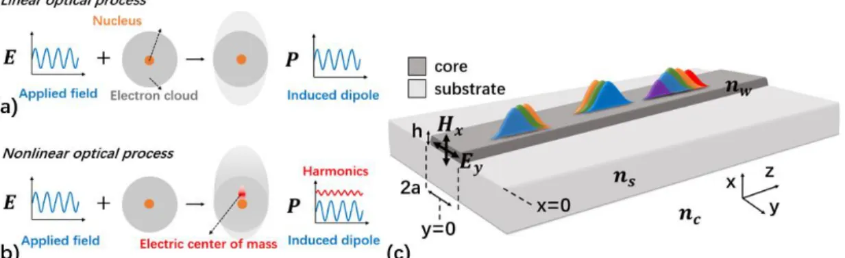
As shown in Figure 6 (a), when light propagates in a linear material, the collection of vibrating dipoles constituting the material results in a linear polarization, while in nonlinear materials (6 (b)), the dependence of the restoring forces with the displacement of the electric charge center of mass leads to nonlinear collection of vibrating dipoles and harmonic waves.
Figure 6. Schematic of light polarization in linear (a) and nonlinear (b) media. (c) Schematic of light
propagating in waveguide with nonlinearities.
Light propagation is governed by the Maxwell’s Equation which consists of four basic equations [7, 8] as below: ∇ × 𝑬 = −𝜕𝑩 𝜕𝑡 (1.1) ∇ × 𝑯 = 𝐽 +𝜕𝑫 𝜕𝑡 (1.2) ∇ ∙ 𝑫 = 𝜌𝑓 (1.3) ∇ ∙ 𝑩 = 0 (1.4)
in which 𝑬 and 𝑯 are vectorial variables of the electric and magnetic fields, respectively, and 𝑫 and 𝑩 are the corresponding electric and magnetic flux densities, respectively. The current density vector 𝐽 and the charge density 𝜌𝑓 represent the sources for electromagnetic field generation. The electric and magnetic fields are bonded with curl revolution, in response to the Gaussian flux of charge density and the local current density while the electromagnetic field is propagating inside the medium. The flux densities 𝐷 and 𝐵 are described by:
𝑫 = 𝜀0𝑬 + 𝑷 (1.5)
14 where 𝜀0 and 𝜇0 are the vacuum permittivity and vacuum permeability, respectively. 𝑷 and 𝑴 are the electric and magnetic polarizations induced by the electromagnetic energy. By taking the curl of equation (1.1) and substituting the curl of (1.2) into it, we can simplify it into
∇ × (∇ × 𝑬) = − 𝜕 𝜕𝑡[∇ × (𝜇0𝑯 + 𝑴 )] = − 𝜕 𝜕𝑡[∇ × 𝑴 + 𝜇0𝐽 + 𝜇0 𝜕 𝜕𝑡(𝜀0𝑬 + 𝑷 )] (1.7) For most of the media we consider in integrated photonics, especially the silicon-based materials, the current densities, charge densities and the magnetic polarizations can be ignored as: 𝑀 = 0, 𝐽 = 0 and 𝜌𝑓= 0. Therefore:
∇ ×(∇ × 𝑬) = −𝜇0 𝜕2
𝜕𝑡2(𝜀0𝑬 + 𝑷 ) (1.8)
This equation is primarily restricted by the boundary conditions ∇ ∙ 𝑫 = ∇ ∙ (𝜀0𝑬 + 𝑷) = 0, which means that crossing the interface between materials the
tangential component of 𝑬 and the normal component 𝑫 should be continuous. For an electromagnetic field propagating through a homogeneous material, the polarization can be written as 𝑷 = 𝜀0𝝌𝑬, by which we have:
𝑫 = 𝜀0𝑬 + 𝜀0𝝌𝑬 = 𝜀0𝜺𝒓𝑬 = 𝜀0𝑛2𝑬 (1.9)
where by definition 𝑛 = √𝜀𝑟 = √1 + 𝝌 is the refractive index of the material, with
linear susceptibility 𝜒. By simply expanding the curl operator in equation (1.8) with 𝛻 ×(𝛻 × 𝑬) = 𝛻(𝛻 ∙ 𝑬) − 𝛻 ∙ (𝛻𝑬) = 𝛻(𝛻 ∙ 𝑬) − 𝛻2𝑬 then equation (1.8) can be simplified as:
𝛻2𝑬 − 𝛻(𝛻 ∙ 𝑬) − 𝜇0𝜀0 𝜕2
𝜕𝑡2(1 + 𝝌)𝑬 = 0 (1.10)
Since ∇ ∙ 𝐷 = 0, and the vacuum light speed is corresponding to 𝜇0𝜀0 = 1
𝑐2, we can further simply it in to into:
𝛻2𝑬 − 1
𝑐2
𝜕2
𝜕𝑡2(1 + 𝝌)𝑬 = 0 (1.11)
With boundary conditions:
∇ ∙ 𝑫 = ∇ ∙ 𝑬 = 0 (1.12)
This is the wave equation for an electromagnetic field propagating in a homogeneous linear material. Typically, electromagnetic wave propagating along the 𝑧 axis with
15 single-frequency 𝜔0 can be described by:
𝑬(𝑧, 𝑡) =1
2𝐹(𝑥, 𝑦)𝐴(𝑧, 𝑡)𝑒
𝑖(𝑘0𝑛𝑧−𝜔0𝑡)+ 𝑐𝑐. (1.13) Where 𝐹(𝑥, 𝑦) is the electromagnetic distribution normal to the propagation direction while 𝑘0 =
𝜔0
𝑐 is the corresponding wavevector while 𝑐. 𝑐. is the complex
conjugate. With 𝜀 = 𝜀0𝜀𝑟 = 𝜀0(1 + 𝜒) , the wave equation generally can be represented, and is also called as the Helmholtz equation as:
∇2𝑬 + 𝑘02𝜀𝑬 = 0 (1.14)
Once nonlinear effects are nonzero, with instantaneous response to electromagnetic
field is [51]:
𝑷 = 𝑃𝐿+ 𝑷𝑵𝑳 = 𝜀0𝜒(1)𝑬 + 𝜀
0(𝝌(𝟐)𝑬 + 𝝌(𝟑)𝑬𝑬 + ⋯ )𝑬 (1.15)
where 𝜺(𝝎) = 𝜀𝐿+ 𝜺𝑵𝑳 = 𝜀0(1 + 𝜒(1)) + 𝜀0(𝝌(𝟐)𝑬 + 𝝌(𝟑)𝑬𝑬 + ⋯ ) , The wave
equation can then be rewritten as: ∇2𝑬 − 1 𝑐2 𝜕2 𝜕𝑡2𝑬 − 𝜇0 𝜕2 𝜕𝑡2𝑃𝐿 = −𝜇0 𝜕2 𝜕𝑡2𝑷𝑵𝑳 (1.16) or ∇2𝑬 + 𝑘02𝜀𝐿𝑬 = −𝜇0 𝜕2 𝜕𝑡2𝑷𝑵𝑳 (1.17)
In equation (1.17) the part on the right can be considered as the electromagnetic source governed by nonlinearities, which is responsible for the generation of new frequencies. For materials with non-instantaneous response, the polarization 𝑃 should be replaced by
𝑷 = 𝜀0∫ 𝝌(𝑡 − 𝑡′) +∞
−∞ 𝐸𝑑𝑡
′ (1.18)
where 𝜒(𝑡 − 𝑡′) represent the non-instantaneous response with time delay 𝑡 − 𝑡′.
In electric polarization 𝑷 = 𝑃𝐿+ 𝑷𝑵𝑳= 𝜀0𝜒1𝑬 + 𝜀
0(𝝌𝟐𝑬 + 𝝌𝟑𝑬𝑬 + ⋯ )𝐸, the
complex first-order susceptibility 𝜒(1) corresponds to the dipole excitations with
bound and free electrons induced by a single photon. The real part of 𝜒1 directly
contributes, as mentioned above, to the real part of the linear refractive index while the imaginary part contributes to the gain and loss from of the material. A remarkable matter of fact for silicon is that due to its crystal structure inversion symmetry, the the
16 second-order susceptibility 𝜒(2) vanishes to zero, strongly restricting the application of this effect for electro-optical modulation and switching.
Third order nonlinearities, on their side involve three electromagnetic waves simultaneously and can be described as follows in optical waveguides:
𝑬(𝑧, 𝑡) = ∑ [1 2𝐹(𝑥, 𝑦)𝐴(𝑧, 𝑡)𝑒 𝑖(𝑘𝑗𝑛𝑧−𝜔𝑗𝑡)+ 𝑐. 𝑐. ] 3 𝑗=1 = ∑ [1 2𝐸𝜔𝑗(𝑧, 𝑡)𝑒 −𝑖𝜔𝑗𝑡+ 𝑐𝑐. ] 3 𝑗=1 (1.19)
With equation (1.15), the polarization governing the third nonlinearity [52] can be represented by multiple terms as:
𝑃𝑁𝐿 =3 4𝜀0𝜒 (3)[|𝐸 𝜔1| 2]𝐸 𝜔1 +6 4𝜀0𝜒 (3)[|𝐸 𝜔2| 2+ |𝐸 𝜔3| 2]𝐸 𝜔1 +1 4𝜀0𝜒 (3)[𝐸 𝜔1 3 𝑒−𝑖3𝜔1𝑡+ 𝑐. 𝑐. ] +3 4𝜀0𝜒 (3)[1 2𝐸𝜔1 2 𝐸 𝜔2𝑒 −𝑖(2𝜔1+𝜔2)𝑡+ 𝑐. 𝑐. ] +3 4𝜀0𝜒 (3)[1 2𝐸𝜔1 2 𝐸 𝜔2 ∗ 𝑒−𝑖(2𝜔1−𝜔2)𝑡+ 𝑐. 𝑐. ] +6 4𝜀0𝜒 (3)[1 2𝐸𝜔1𝐸𝜔2𝐸𝜔3𝑒 −𝑖(𝜔1+𝜔2+𝜔3)𝑡+ 𝑐. 𝑐. ] +6 4𝜀0𝜒 (3)[1 2𝐸𝜔1𝐸𝜔2𝐸𝜔3 ∗ 𝑒−𝑖(𝜔1+𝜔2−𝜔3)𝑡+ 𝑐. 𝑐. ] (1.20)
where, on the right side, the first and second terms correspond to the self-phase modulation (SPM) and cross-phase modulation (XPM) effects, respectively. An illustrative picture of the main classical third-order mechanisms is presented in Figure 7.
17
Figure 7. Schematic of nonlinear process, reproduced from [14].
1.2.2 Silicon plasma dispersion and Pockels effects for light modulation
Second-order nonlinearity 𝜒(2)is preferably expected for optical modulation in most of photonic platforms. The Pockels effect indeed traditionally makes it possible to obtain a variation in the optical refractive index by applying an RF electric field, i.e. by simply applying a modulation RF voltage after manufacturing a set of metal electrodes judiciously placed on either sides of the waveguides. Though 𝜒(3) can be considered for light modulation, difficulties stem from the request of strong power for driving the modulator since the on-chip modulators are basically driven by a radio-frequency (RF) electrical source. As this 𝜒(2) effect is absent in bulk silicon due to the centro-symmetry of crystal lattice in silicon, it has proved necessary to exploit another phenomenon, which has finally turned out to be simply based on an essential property of silicon: it is a semiconductor and is therefore characterized by a possible transport of free charges (electrons and holes) induced by doping and modulable by the application of a voltage (PN junction).
1.2.2.1 Plasma dispersion effect and modulator
As mentioned above, free carrier concentrations can be modulated in silicon waveguide by the use of a PN junction, i.e. relying on the so-called plasma dispersion effect. In turn, the modulation of the free carrier plasma is responsible for the modification of the material conductivity, which leads to a simultaneous change of the real (∆𝑛) and imaginary parts (∆𝛼) of the refractive index. Preferentially playing on one or the other of these contributions leads to the classification of electro-optical modulators into electro-refraction or electro-absorption modulators.
Quantitatively [53]:
∆𝑛 = ∆𝑛e+ ∆𝑛h = −[8.8 × 10⁻²²∆𝑁e+ 8.5 × 10⁻¹⁸(∆𝑁h)0.8] (1.21)
18 where ∆𝑁e,h are the variations of the electron and hole concentrations, while ∆𝑛e,h
is the index variation induced by the electrons/holes. ∆𝛼e,h shares the similar definitions. Electrical manipulation of the carrier density interacting with the propagating light is achievable through mechanisms categorized as carrier injection, carrier accumulation or carrier depletion. The difference of these free methods is shown in Figure 8. As the most preferred mechanism, carrier depletion provides most promising electro-optic bandwidth due to most effective carrier motion from filling to vanishing, controlled by reverse electric field. In practice, an electrical polarization structure must be designed and realized (PN junction, MOS capacitance: Figure 9 (a), [54]) and an interferometric structure must be implemented for electro-refraction modulators (Figure 9 (b), [55]).
Figure 8. Schematic of silicon modulators using carrier-accumulation (a), carrier injection (b) and
carrier depletion (c) effects. Figures are reproduced from [67].
Figure 9. Schematic of silicon modulators using Mach-Zehnder Interferometer (a) and ring resonators
(b). Figures are reproduced from [68] and [69].
1.2.2.2 Strain-induced Pockels effect and optical modulation
In addition to the plasma dispersion effect, a new emerging and interesting approach reported in the last decade is the strain induced Pockels effect in silicon [56]. This topic has drawn lots of attention from the silicon photonics community since it presents two important merits: an ultra-fast modulation capability based on the Pockels effect (removing the contribution of free carriers removes the carrier transport
19 transit time blockade) and a simple fabrication and integration (as no PN junction if then needed). The basic idea of this approach is to break the centro-symmetry of bulk silicon by straining its lattice unit cell through the use of straining external layers [57], as shown in Figure 10, for producing non-zero 𝜒(2).
Figure 10. Schematic of straining host lattice with external material. Cases with different
tensile/compressive strain are distinguished by the arrows.
Figure 11. Schematic (a) and performance (b) of strained silicon modulator. Figures are reproduced
from [63].
This technique to generate 𝜒(2) in silicon has been theoretically as well as experimentally investigated in the past years. Interestingly, the strain induced 𝜒(2) was first strongly overestimated in early works where the contributions of the Pockels and carrier effects were not properly separately estimated [58-60]. New works performed later in 2014 and 2015 corrected this trend [61,62], and a first high-speed (up to 20GHz) characterization was then demonstrated in 2018 [63] using the silicon-nitride-on-silicon platform. In this demonstration (Figure 11), a long (2mm) Mach-Zehnder interferometer was adopted in a first approach to estimate for the electro-optical response that turned to be around -1.8 pm/V in still non-optimized structures.
Further work is needed in this direction to improve and strengthen the observed effects. We will come back to this point later in this manuscript.
20
1.2.2.3 Demand in addressing the power-bandwidth trade-off
The universal motivation for reducing the power consumption and increasing the modulation efficiency has never been stopped and triggered for novel modulation approaches. The reason is that the index change resulting from the application of a control voltage is relatively small, usually by a few 10-5, or by a few 10-4 at most. As a result, this places relatively high constraints on the interferometric structure in charge of converting index modulation into intensity modulation with high modulation contrast. A first option is to use a very long interferometer (typically an MZM of a few mm [64, 65]), so that the interaction length compensates for the low index modulation. To circumvent this drawback, another option is to enhance light matter interaction by the use of high Q resonators. One of the common methods is to use ring resonators in this purpose. Numerous works have contributed to silicon ring modulators [66, 68, 55]. In addition to ring resonators, PhC slow-light waveguides (Figure 12(a)) have also been adopted to enhance light-matter interactions, with slow light group velocity engineering. Almost ten-times higher efficiency was demonstrated with one tenth footprint in such structures [68, 69]. In addition to waveguides, 2D PhC cavities (Figures 12(c) and (d)) have also been considered for light modulation [70] with ultra-low powers (few μW) required for reasonable extinction ratio (ER, 10dB).
Comparisons between these modulators are presented in Table 1. As it can be seen, both ring resonators and PhC cavities can enhance modulation efficiency by providing much larger wavelength shifts when identical driven swings are applied to them. However, at the same time, the high photon lifetime resulting from the outstanding resonance (Q>>103) in return restricts the achievable electro-optic
bandwidth. This power-bandwidth trade-off has been witnessed [66, 67] experimentally and especially when quality factor is raised up to hundreds of thousands, the modulation speed is then limited to no more than few GHz [70, 71]. Another point is that a higher-Q resonator normally indicates a bigger active volume and in return a reduction of the efficiency which can be improved by compressing the device volume [55]. Though high-bandwidth silicon PhC cavity modulator has not been experimentally demonstrated, some recent theoretical works on silicon photonic crystal cavity modulators [72-74] indicated promising results (Figure 12(e)) [75] to beat this limit, which yet remains essentially unsolved.
Therefore, to universally improve silicon resonant modulator and especially promote the strain silicon platform, the power-bandwidth need to be addressed.
This leaves us the first issue that we will address in chapter 2, with subwavelength engineering of 1D photonic crystal cavities.
Type Electrical bandwidth Eye diag. Extinction ratio (dB) Efficiency V*cm Quality factor Drive swing Vpp (V) Length /diameter μm Silicon, 60 Gbps 7.4 2.3 - 5.75 800
21 depletion M.-Z. [64], [65] 25 Gbps 5 1.15 3.3 1000 Silicon, depletion PhC M.-Z. [68], [69] 10 Gbps 25 Gbps 7.9 > 6 0.056 - - 4.2 3.5 200 200 Silicon, depletion Ring [66], [67], [67] 10 Gbps 25 Gbps 25/40 Gbps 8 7 8 50 fJ/b 0.76 0.9 fJ/b 14500 7500 ~ 3000 2 2.3 0.5/2.2 30 >100 4.8 Silicon, PhC cavity [71], [72] ~ GHz 20 GHz 10 6 ~ μW 14 AJ/b 5.4e5 8500 1.5 0.6 ~10 2 Strained Silicon, M.-Z. [63] A21, 10GHz > 3 - 2 mm 20 2000
Table 1. Comparison between different kinds of silicon electro-optic modulators.
Figure 12. Schematic of silicon PhC slow-light Mach-Zehnder modulator (a) and nanobeam cavity (b)
with optical bistability. (c) and (d) schematic of a 2D PhC cavity silicon modulator. (e) schematic of a 2D PhC cavity silicon hybrid modulator. Figures are reproduced from [69], [74], [71], [71] and [75].
22
1.2.3 Silicon optical Kerr effect and nonlinear frequency generation 1.2.3.1 Optical Kerr effect and Two-photon absorption in silicon
As mentioned above, silicon is not a material naturally suited for electro-optical modulation. On the other hand, it has a strong third order non-linearity which potentially opens up a wide field of exploitable phenomena, starting with the four-wave mixing processes (FWM), and therefore the possibility of parametric amplification, wavelength conversion, etc. Our enthusiasm must be somewhat tempered by a significant penalty related to the phenomenon of two-photon absorption, as we will see, affecting wavelengths below 2.2µm but yet not beyond.
Generally speaking, the Kerr effect can be described as follows:
𝑃 = 𝑃𝐿+ 𝑃𝑁𝐿 = 𝜀0(𝜒(1)+ 3𝜒(3)|𝐸|2)𝐸 (1.23)
With the definition 𝑛 = √𝜀𝑟, the refractive index, including the nonlinearity-induced
absorption, can be represented (with the assumption that the nonlinear susceptibility is much smaller than the linear counterpart) as:
𝑛 = √𝜀𝑟 = √(1 + 𝜒(1)+ 3𝜒(3)|𝐸|2) ≈ √(1 + 𝜒(1)) +
3𝜒(3)|𝐸|2
2(1+𝜒(1)) (1.24) Since 𝑛1 = √(1 + 𝜒(1)) is the linear material refractive index, then equation 1.22
can be simplified as: 𝑛 = 𝑛1+ 3𝜒(3)|𝐸|2 2𝑛1 = 𝑛1+ 3𝜒(3) 4𝑛12𝜀0𝑐(2𝑛1𝜀0𝑐|𝐸| 2) (1.25)
By expanding 𝜒(3) into its real and imaginary part, the refractive index 𝑛 can be
rewritten as: 𝑛 = 𝑛1+ 𝑛2𝐼 + 𝑖α2𝐼 (1.26) where 𝑛2 = 3 4𝑛12𝜀0𝑐𝑅𝑒(𝜒 (3)) and α 2 = 3 4𝑛12𝜀0𝑐𝐼𝑚𝑎𝑔(𝜒 (3)) is the nonlinearities
induced index change and absorption, respectively.
Kerr effect is very strong in silicon, with 𝑛2 = 3 × 10⁻¹⁸𝑚2/𝑊, i.e. is a factor of
100 higher than in silica fibers, which promises silicon as a solid candidate for on-chip light conversion and generation. Yet, as shown in Figure 7, the couple of pump photons do not only contribute to the Kerr-induced SPM effect, but also to the two-photon absorption (TPA) process. This phenomenon occurs non-negligibly in the near-infrared wavelength region due to the fact that the double of the photon energy can easily surpass the energy gap between the valence and conduction bands. This effect typically influences the degenerate FWM (𝜔𝑃2= 𝜔𝑃1) by sacrificing part of the pumping photon for higher energy conversion without direct optical repay. Due to the non-negligible TPA (Figure of merit FOM = 𝑛2
23 𝛽2 = 5 × 10⁻¹²𝑚/𝑊 in the O band (around =1550nm), light all-optical modulation and wavelength conversion are hindered with threshold powers of few mW only. This absorption contribution has also to be integrated into α2 in equation (1.26).
In addition to the direct absorption behavior, the absorbed photons can in return, produce new free carriers with long lifetime leading to free-carrier absorption (FCA) and free-carrier index (FCI) changes. This combination of TPA and the long lasting FCA jointly work against the FWM by reducing the parametric gain and slow down the bandwidth of silicon Kerr switches. However, some methods can be applied that can effectively reduce the influence of FCA and TPA. For example, an external electric field produced by PN junction can be used to deplete the free carrier while ultrafast pump will temporal scale faster than the TPA process suppress TPA. The simplest approach to eliminate TPA and FCA is also to perform the nonlinear processes with a pump wavelength larger than 2.2 μm since the double of the photon energy then no longer reaches the Si bandgap. Impressive results have been obtained by this approach, that yet does not solve the need for telecom wavelength all-optical signal processing techniques.
1.2.3.2 Four-wave mixing enhanced by resonators and photonic crystal
Four-wave mixing has a wide range of applications including parametric amplification, wavelength conversion, nonlinear microscopy and spectroscopy, etc. Particularly, light amplification in silicon has been demonstrated using FWM [76] for more than a decade. Unlike the Raman effect which is restricted by the availability of the phonons in materials, the FWM effect is able to provide a larger parametric amplification in a broader wavelength range. The needed elements for these parametric amplifications are the fine control of the involved waves phase matching condition and the realization of low waveguide propagation losses. Starting from the energy conservation (𝜔𝐼 = 𝜔𝑃2+ 𝜔𝑃1− 𝜔𝑆) being satisfied, the phase matching condition is described by the condition of involved wavevectors as: ∆𝛽 = 𝛽P1 +
𝛽P2− 𝛽S− 𝛽I= 0. In this condition, 𝑆, 𝐼, 𝑃1 and 𝑃2 are labels with respect to the signal, the idler, and the pump waves, respectively. This condition typically requires careful dispersion engineering of the waveguide cross-section. In the control of phase matching, not only the waveguide dimensions controlling its chromatic dispersion, but also the nonlinearities-induced phase variation needs to be taken into account. This is where SPM or XPM in that Kerr nonlinearities are widely used for ultrafast phase modulation, which can be translated into intensity modulation with the assistance of Mach-Zehnder interferometers or micro resonators. Using optimized designs, different kinds of applications have been demonstrated, such as near-infrared broadband optical parametric gain [76, 77] (see Figure 13).
In order to enhance the nonlinear light-matter interaction, ring resonators were adopted for simultaneously making three waves circulate with a self-aligned frequency spectrum [77, 78]. Similar works were also performed in multi-resonant PhC cavities (see Figure 14) for further improvement of the light-matter interaction
24 within ultra-small active volumes [79, 80]. By introducing the coupled mode scheme to produce parity-varied eigen modes in photonic molecules [81-83], new freedom was given to control FWM. This photonic molecule was also found to be able to improve the light-matter interaction with a mis-alignment cavity lattice [84].
Figure 13. (a) Schematic of silicon degenerate four-wave mixing (b) Frequency spectrum of (a).
Figures are reproduced from [76] and [77].
Though resonators are powerful in promoting strong light-matter interaction, the resonant nature of these cases however puts difficulties on the broadband or tunable functions which are highly expected in practical applications. In this context, PhC slow-light waveguides [85] were applied to improve the light-matter interaction [86] while leaving access to broadband purpose (see Figure 15). Based on this method, third-order harmonic generation (green light) based on silicon Kerr effect was demonstrated [87]. Numerous works on group velocity control for enhancing silicon Kerr nonlinearities using photonic crystal waveguides have been later reported [88, 89].
25
Figure 14. Methods of enhancing the silicon four-wave mixing with (a) ring resonator, (b)
multi-resonance PhC cavity, (c) coupled rings molecule and (d) coupled PhC molecule. Figures are reproduced from [77], [79], [81], [83].
Figure 15. (a) Schematic of 3rd harmonics in silicon enhance by photonic crystal slow-light waveguide.
(b) Microscope of silicon slotted photonic crystal slow-light waveguide. (c) Schematic and (d) performance of using photonic crystal slow-light waveguide to enhance four-wave mixing. Figures are reproduced from [87], [89], [85], [85].
1.2.3.3 Demand in flexible dispersion control
As was introduced above, the Kerr nonlinearities highly depend on the energy conservation and phase matching conditions, no matter classical strip waveguides or PhC waveguides are considered. In this context, careful waveguide dimension design for controlling the waveguide dispersion to compensate the nonlinear phase induced-mismatch [90] is necessary and important. However due to the fact that semiconductor platforms, especially silicon, present a high core/cladding index-contrast, standard waveguides normally exhibit sharp dispersion changes (see Figure 16 (a)). These unflatten dispersion behaviors intrinsically lead to narrow bandwidths of the conversion wavelength range, as shown in Figure 16 (b). Similar results are also found at longer wavelengths around =2 microns [91]. Photonic crystal patterns are able to offer flexible engineering capability of the waveguide dispersion but also bring another drawback with their huge sensitivity to changes of the light group velocity dispersion and to the fabrication techniques, as shown in Figure 15 (c) and (d).
26 This issue on dispersion control gives us another question: Do we have more
robust and flexible methods to engineer the dispersion for simultaneously fulfilling energy conservation and phase matching conditions?
Figure 16. (a) Dispersion of silicon waveguide with different cross-section and (b) Corresponding
conversion efficiency of four-wave mixing. Figures are reproduced from [90].
1.3 Subwavelength structures at the services of passive and
active functions
To address those two issues laid on section 1.2.2.3 and 1.2.3.3, i.e. the power-bandwidth trade-off in a silicon resonant modulator and the management of waveguide dispersion in silicon waveguides to enable phase-matched nonlinear optical processes, we think that subwavelength waveguide structures can bring a decisive help. Based on subwavelength optics, we expect, from a novel point of view,
to address those issues, improve device performances and open new opportunities for the relevant applications.
1.3.1 Subwavelength structures: a powerful tool for passive devices
Subwavelength optics has been proposed for more than two decades [92] and benefits from the rapid development of fabrication technologies which makes it accessible experimentally. Subwavelength optics [92] has found many applications in the realization of vertical cavity surface emitting lasers [93-96] where light penetration length and photon life are dramatically reduced with this approach and
27 tunable functions can be realized when combined with MEMS technologies. In addition to membrane mirrors, subwavelength structures can be also applied to develop meta-surfaces [97], non-conventional optical lenses [98], holographic and nonlinear devices [99], as well as on-chip photonic mode convertors [100], to quote a few examples.
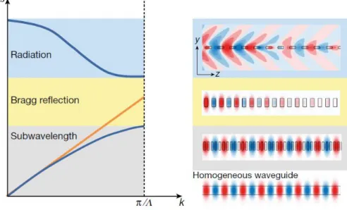
In a photonic crystal perspective (see Figure 17), sub-wavelength photonics occurs in fact when light frequency is much smaller than the period of a periodic structure (at least locally periodic), meaning a much larger wavelength than the geometrical corrugation scale ( 𝐴 ) that 𝜆 ≫ 2𝑛𝐴 (where 𝑛 is material index). Spatially averaging the optical material properties then becomes relevant. Band structure and the dispersion curves of periodic structures waveguide are shown in Figure 17 for comparison. In this context, the diffraction (Mie scattering, radiation, Bragg reflection) is strongly suppressed and especially when they are much larger than the pitch, the particles work like Rayleigh scatters. In this situation the stratified structure behaves like a homogeneous anisotropic material with an equivalent anisotropic permittivity tensor with respect to the macroscopic electromagnetic field [92], which has been discussed 50 years ago. It was difficult to conduct experiments in the visible or near-infrared ranges but of the progress of micro fabrication has rapidly reduced this limitation (e.g. with electron-beam lithography and other techniques) in the last 15 years
Figure 17. Schematic of the optical response in different regions of periodically structured waveguide.
Figures are reproduced from [102].
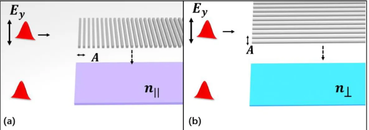
In [92], Dr. Rytov found that if the period of subwavelength structures consisting of alternating slabs of dielectric materials with refractive indices 𝑛H and 𝑛L is much smaller than the incident wavelength, the overall medium is optically equivalent to a uniaxial crystal with an optical axis perpendicular to the layers (see Figure 18). With a quasi TE light polarization injection, if the segment is arranged along the propagation
28 direction (i.e. polarization is parallel to periodical interface) or the normal direction (i.e. polarization is perpendicular to the periodic interface), the global photonic structure can be considered as a homogeneous material with an index being [101-103]: Either 𝑛||2 = 𝑤 𝐴𝑛𝐻 2 + (1 −𝑤 𝐴)𝑛𝐿 2, (1.27) Or 𝑛ꓕ−2= 𝑤 𝐴𝑛𝐻 −2+ (1 −𝑤 𝐴)𝑛𝐿 −2, (1.28)
where 𝑛II and 𝑛ꓕ are the equivalent material index values in the two considered
cases, with 𝑛H and 𝑛L standing for the high-index and low-index materials, respectively. The pitch and the filling factor of the high-index segment are called here 𝐴 and 𝑤/A , respectively. With this approximation, index-engineering is available for creating artificial media being designed to have a greater range of material properties than those available in nature.
Figure 18. Schematic of the equivalence of periodically structures, for electric field polarizing parallel
and perpendicular to periodic surface.
These “all-dielectric metamaterials” bring new degrees of freedom in the design space parameter of optical waveguide structures, for the purposes including splitter, coupler [104-106], biosensing [107], inverse photonic designs [108, 109], automatic calculation [110, 111], etc. Unlike the typical bulk metamaterials, these “all-dielectric metamaterials” are integrated easily with the on chip photonic component using planar fabrication technologies (see Figure 19), with numerous advances, which are the reason why they are so interesting.
29
Figure 19. (a) Schematic of subwavelength structured silicon grating coupler. (b) Schematic and
scanning electron microscopy image of subwavelength broadband beam splitter. (c) Scanning electron microscopy image of subwavelength spot convertor. (d) Scanning electron microscopy image of a polarization beam splitter using inverse design. Figures (a), (b), (c) and (d) are reproduced from [104], [105], [106] and [109].
1.3.2 Subwavelength engineering: a toolbox to help light-matter interaction
The powerfulness of subwavelength engineering has been witnessed [93-111] and introduced in section 1.3.1. This is a take-home message that we expect to use subwavelength engineering to address those two issues laid on section 1.2.2.3 and 1.2.3.3: i.e. power-bandwidth trade-off in a (strained) silicon resonant
modulators and the dispersion manipulation for exploring Kerr-induced optical effects in silicon waveguides (with a special focus, as shown later on FWM and frequency comb generation).
✓ In chapter 2, we will first address the power-bandwidth trade-off using subwavelength engineering to enhance efficient light modulation in silicon photonic crystal (Fano) cavity silicon resonant modulators.
✓ In chapter 3, we will introduce a method (called “Self-Adaptive Boundary” (SAB)) for flexibly controlling waveguide dispersion and enabling an automatic FWM phase matching condition. Taking its root from ideas derived from quantum mechanics and being practically achieved by the use of subwavelength waveguide structures, this method will be applied to waveguide FWM processes and frequency comb generation. Soliton comb
30 generation and dynamics will be studied in the engineered waveguides based on the nonlinear Schrödinger equation in the form of the Lugiato-Lefever equation.
We believe that the proposed method opens even wider perspectives for the exploitation of 3rd-order non-linear optical properties from the silicon photonic platform or any other platform (IIV/V semiconductors, polymers, etc). The story began on this background but will definitely not limited in just nonlinear optics and subwavelength optics and cases we mentioned. The hint among all these contents is, the flexible control of light-matter interaction. Harnessing these preliminary researches presented following, we hope new visions can be reached for our further researches in nonlinearities-based photonics and other researches including quantum light source, on-chip spectroscopy, on-chip temporal signal control etc.
31
2 Subwavelength structures for enhanced
electro-optical modulation
In this chapter, we first explain the bandwidth-consumption trade-off in silicon
resonant modulators and indicate that by sharping the resonant spectrum of the in-modulator constitutive resonator, modulation efficiency can be improved without sacrifice on the bandwidth. More specifically, we will describe the mechanism based
on a subwavelength engineering approach to produce an asymmetric-spectrum Fano
resonance in a single nanobeam cavity, i.e. made on a single optimized strip silicon
waveguide channel. Analytical analysis will be presented to sustain the proposed idea and, with the parameters derived from the design, fabrication and characterization results will be presented, before concluding.
Next, the design of a strained silicon modulator based on this single-waveguide subwavelength structured Fano resonator will be developed. In addition, we will indicate how a wavelength tunable operation can be achieved with such a single-waveguide resonator through both analytical and experimental demonstrations.
Overall, the feasibility of high-bandwidth low-consumption silicon resonant modulators will be reported, with outlook of tunable function and new application using this subwavelength structured resonator.
2.1 Sharpening the resonant spectrum of PhC Fano
cavities with subwavelength structures
2.1.1 Introducing a Fano resonance to a single-waveguide resonant cavity
As we introduced it above, micro-resonators (including micro rings/disks and photonic crystal cavities) are capable for small footprints and relatively small off/off operation (typically > 15dB) in on-chip integrated configurations [112]. However, the considerable photon lifetime in an ultra-high-quality factor (Q>>103) cavity is
detrimental to the target modulated bandwidth (at least >10GHz). Generally speaking, the photon dynamics in a Lorentzian shape cavity modulator fed directly by a bus can be understood as it is shown in Figure 20. Since the cavity we consider here is a nanobeam cavity (one of 1D photonic crystal cavities) fed directly by a bus waveguide, as Figure 20 (b), Lorentzian shape with highest transmission on resonance is shown in Figure 20 (a).
32
Figure 20. (a) Schematic of on/off-resonance photon dynamics. (b) Schematic of a nanobeam cavity
based on a strip optical waveguide drilled by holes. (c) Schematic of in-complete light extinction in high-Q and low-Q case.
In such a cavity, strong light reflection is formed for a wideband spectrum and only light wave with on-resonant frequency can be transferred to the cavity core, with an in-cavity optical power built up, and then remitted to the output port. The on/off modulation operation is obtained at a specific wavelength by shifting the cavity resonance from an “on-resonance” to “off-resonance” thanks to any relevant possible mechanism (e.g. thermal effect, electro-optical and other nonlinear effects, free carrier plasma dispersion effect). As the cavity energy decay time is proportional to Q (where photon lifetime which determined by time duration for a power decay factor of 𝑒−2.)
A long-lasting output energy decay of a high-Q cavity can be actually observed and lead to non-instantaneous transition on modulator (see Figure 20 (c)). Given a certain spectrum shift that determined by materials and applied signal, the “high-Q” spectrum can give a larger “accessible (maximum) extinction ration” (or to say, transmission contrast) than that of “low-Q” spectrum. This high accessible contrast can give the possibility for reducing the required driven power. However, as the Figure 20 (c), this large contrast cannot be fully used since photons decay is cut at next raising/falling edge of the driven signal. In contrast, though smaller maximum extinction ratio is obtained with a low-Q spectrum, but full light falling back then occurs before the signal flip.
For example, for a quality factor of only 104, the bandwidth 𝑓
3dB limited by
photon lifetime (with negligible RC constant) can be calculated as: 1
𝑓3𝑑𝐵2 = (2π𝜏) 2+
(2π𝑅𝐶)2 ≈ (2π𝜏)2 and 𝜏 =𝑄 𝜔 =
𝜆𝑄
33 working wavelength at around 1.5𝜇𝑚 [66]. Though the experimental bandwidth is later found can be a bit larger than this estimation [112], resonators designed for high bit rate modulators have usually limited Q factors of a few thousands [113, 114]. Such a limit on Q factors leads to the request of higher driving swing for enlarging the wavelength shift and the accessible extinction ratio compared to a higher-Q cavity. This has no doubt caused a larger power consumption, e.g. of tens to hundreds of femtojoules per bit for acceptable extinction ratio (>8 dB). Various approaches like different-signal driving [115] and vertical P-N structures [116] for silicon disk resonators have been implemented to reduce power consumption. However, these kinds of doping schemes are complex and challenging with respect to fabrication accuracy control. Therefore, new and simple solutions are expected for low power consumption and high-bit rate optical modulation.
In fact, modulation inefficiency comes largely from the shape of the spectral resonance used, very symmetrical, and which therefore implies to be significantly shifted in frequency in order to induce an on/off extinction ratio >>1. If we can,
as illustrated in Figure 21, rotate the Lorentzian-lineshape spectrum without any increase on the Q factor, we can take advantage of the fast light response and simultaneously improve the obtained modulation extinction ration (ER). This is the reason why Fano resonances, which arise from the interference of a discrete resonant mode and a continuum background, have been proposed to solve this issue [117]. As it is shown hereafter and already illustrated in Figure 21, their asymmetric spectrum signature can be used to address the bandwidth-power trade-off of silicon resonant optical modulators and potentially minimize the power consumption of silicon switching and modulation devices. Different types of Fano-resonance-based cavities have already been proposed including spatial membrane structures [118], plasmonic resonators [119] and integrated side-coupled one/two-dimensional (1/2D) photonic crystal cavities [120-123]. Thanks to the advances of fabrication technology, novel integrated devices based on these Fano cavities like nonreciprocal transmission structures [124], Fano lasers [125] and switches [126] have been demonstrated. Especially, an all-optical high-bit rate modulation behavior combining the free carrier response of indium phosphide and a Fano cavity was demonstrated[127].
![Figure 2. Future evolution and applications in silicon photonics, reproduced from [6]](https://thumb-eu.123doks.com/thumbv2/123doknet/14529190.723301/11.892.146.754.471.845/figure-future-evolution-applications-silicon-photonics-reproduced.webp)
![Figure 4. Main challenges and technical breakthroughs in silicon photonics, reproduced from [3]](https://thumb-eu.123doks.com/thumbv2/123doknet/14529190.723301/13.892.136.753.333.654/figure-main-challenges-technical-breakthroughs-silicon-photonics-reproduced.webp)

![Figure 22. Schematic views, dispersion diagrams and mode profiles of PhC cavities reproduced from [131] and [137]](https://thumb-eu.123doks.com/thumbv2/123doknet/14529190.723301/36.892.143.751.630.932/figure-schematic-views-dispersion-diagrams-profiles-cavities-reproduced.webp)

