Publisher’s version / Version de l'éditeur:
Vous avez des questions? Nous pouvons vous aider. Pour communiquer directement avec un auteur, consultez la
première page de la revue dans laquelle son article a été publié afin de trouver ses coordonnées. Si vous n’arrivez pas à les repérer, communiquez avec nous à [email protected].
Questions? Contact the NRC Publications Archive team at
[email protected]. If you wish to email the authors directly, please see the first page of the publication for their contact information.
https://publications-cnrc.canada.ca/fra/droits
L’accès à ce site Web et l’utilisation de son contenu sont assujettis aux conditions présentées dans le site LISEZ CES CONDITIONS ATTENTIVEMENT AVANT D’UTILISER CE SITE WEB.
ACS Applied Materials and Interfaces, 11, 39, pp. 36027-36034, 2019-09-18
READ THESE TERMS AND CONDITIONS CAREFULLY BEFORE USING THIS WEBSITE.
https://nrc-publications.canada.ca/eng/copyright
NRC Publications Archive Record / Notice des Archives des publications du CNRC :
https://nrc-publications.canada.ca/eng/view/object/?id=461ce9a5-6ac6-4a66-8406-00c3da7e0cdc https://publications-cnrc.canada.ca/fra/voir/objet/?id=461ce9a5-6ac6-4a66-8406-00c3da7e0cdc
NRC Publications Archive
Archives des publications du CNRC
This publication could be one of several versions: author’s original, accepted manuscript or the publisher’s version. / La version de cette publication peut être l’une des suivantes : la version prépublication de l’auteur, la version acceptée du manuscrit ou la version de l’éditeur.
For the publisher’s version, please access the DOI link below./ Pour consulter la version de l’éditeur, utilisez le lien DOI ci-dessous.
https://doi.org/10.1021/acsami.9b09857
Access and use of this website and the material on it are subject to the Terms and Conditions set forth at
Polymer encapsulants for threshold voltage control in carbon nanotube transistors
Polymer Encapsulants for Threshold Voltage
Control in Carbon Nanotube Transistors
François Lapointe1*, Ashish Sapkota1,2, Jianfu Ding1, Jacques Lefebvre1
1. National Research Council Canada, 1200 Montreal Road, Ottawa, Ontario, Canada, K1A 0R6 2. Department of Printed Electronics Engineering, Sunchon National University, Sunchon 540-742, Korea
ABSTRACT. While carbon nanotube transistors present outstanding performances based on key metrics, large-scale uniformity and repeatability required in printable electronics depend greatly on proper control of the electrostatic environment. Through a survey of polymer dielectric encapsulants compatible with printing processes, a simple correlation is found between the measured interfacial charge density and the onset of conduction in a transistor, providing a rational route to control the electrical characteristics of carbon nanotube transistors. Smooth and continuous balancing of the properties between unipolar p type and n type transport is achieved
using a molar fraction series of poly(styrene-co-2-vinylpyridine) statistical copolymers combined with an electron donating molecule. We further demonstrate the easy fabrication of a p-n diode
which shows a modest rectification of 8:1.
KEYWORDS: carbon nanotubes ; field-effect transistors ; polymer dielectrics ; encapsulation ; electric transport ; doping ;n type transport ; printed electronics
INTRODUCTION
Progress in semiconducting single-walled carbon nanotubes (sc-SWCNTs) purification and enrichment1,2 enables the low-cost and large-area fabrication of soft, flexible,3,4 stretchable and transparent5 electronic devices—logics,6,7 displays,8 sensors,9–12 and even more complex systems such as electronic skin13 and three-dimensional integrated circuit architecture14—from solution
processes and printing techniques. Functional components necessitate the control of parameters beyond current carrying capabilities and on/off ratio: The performances of such devices are tributary to the carrier mobility, the operation power, and their device-to-device variations. Moreover, control over the carrier type allows the creation of complementary integrated circuits. SWCNT devices are, however, sensitive to external interferences and exhibit unipolar p type
conduction under normal conditions, with O2 adsorption inducing a Schottky barrier that
suppresses electron injection at metal-SWCNT contacts15,16 and with the O
2 / H2O redox couple
that hinders electron transport in the channel.17
A widely used solution to mitigate the effects of ambient gases consists of encapsulating the device under a dielectric coating.18 The coating layer can be subject to uncontrolled electrostatics
as a result of incomplete stoichiometry and traps, while high κ dielectrics also display interfacial dipoles because of the presence of polar chemical groups,19 with consequences on the carrier
type, mobility, and threshold voltage. The intentional tuning of the coating layer bulk and interfacial charge density can be exploited to control the device properties, even yielding unipolar n type conduction.20–23 Nevertheless, there remains a technological gap as inorganic
coatings are not adapted to printing techniques due to high temperature, vacuum processing, while most polymer coatings reported to date are either hydrophilic23 or yieldp type devices.24
The threshold voltage VT is a key metric of field-effect transistor (FET) characteristics
reflecting the flat band potential and built-in electric fields due to fixed charges in the proximity of the channel active material. As a quantitative metric of a FET turn-on voltage, VT is closely
related to the operation mode (depletion or enhancement) and operation power. In this work, we surveyed more than 20 polymers with moderate to high degree of hydrophobicity for carbon nanotube network field-effect transistor (CNN-FET) encapsulation,24,25 affording control over the threshold voltage and other characteristics parameters by rational selection of passivation materials and their combinations. We report a simple linear relationship between VT and the
charge accumulated at the immediate carbon nanotube interface. With a better handle on the electrostatic environment and associated charge trap density, reduced day-to-day and device-to-device variations can be expected. Poly(2-vinylpyridine) (P2VP) was found to produce the most negative threshold voltage for hole transport while polystyrene (PS) had amongst the most positive. A combination of the two polymers in a blend or as copolymers allows a continuous tuning of transistor parameters. Moreover, the addition of an electron-donating molecule, 4-(2,3-dihydro-1,3-dimethyl-1H-benzimidazol-2-yl)-N,N-dimethylbenzenamine (N-DMBI), to P2VP converts an ambipolar transistor to an air stable unipolar n type one. This simple materials
combination is a concrete solution to the complementary p and n type transistors required to
implement logic gates in printable electronics, in analogy to CMOS devices. This work is readily transferrable to printing in ambient as a low temperature process for low-cost and flexible electronics.
RESULTS AND DISCUSSION
Figure 1. (a) Schematics of an encapsulated CNN-FET. (b) Schematics of the charge measurement setup (left) and the probe setup (right).
In order to simplify our study, we chose the prototypical bottom gate transistor configuration on SiO2/Si [Figure 1(a)]. With this architecture, the gating action is decoupled to a great extent
from the encapsulation layer19 and various encapsulating polymers can be studied without a precise knowledge of layer thickness. This is in contrast with a top gate configuration where the top dielectric layer also acts as the gate dielectric and interfacial dipoles perturb charge transport.19 We note that conclusions drawn here should be valid and therefore be tested for top gated devices. Our strategy also circumvents large differences in SWCNT surface coverage that may arise when preparing the random network on bottom gate polymer dielectrics with various surface energies.
We first set to test the hypothesis that the triboelectric effect, or the tendency of a material to pick up a charge through contact or friction, has an influence on the charges present at the CNT / dielectric interface and thus alters the characteristics of CNN-FETs. With this goal in mind, we
selected two polymers in the triboelectric series where the first should pick up mainly negative charges while the second should have a positive charge uptake. Based on availability and chemical similarity, we chose PS as the “negative” polymer and P2VP as the “positive” one.26 We tested two approaches to build series with varying fractions of the monomers: simple blending of PS and P2VP and statistical copolymers of the respective monomers. We present here only the results of the latter. The blending results are similar, albeit with more dispersion in the data, and are available in the Supp. Info. (Figures S4 to S7). Statistical copolymers were thus acquired at different molar fractions of the styrene (S) and 2-vinyl pyridine (2VP) monomers (11.5, 25, 40, 70 2VP mol%). The end points of the series were the homopolymers (0%: pure PS and 100%: pure P2VP).
A series of CNN-FETs were prepared on SiO2/Si (Fraunhofer chips, Gen 5, 230 nm oxide,
channel dimensions: 20 × 2000 μm) and the transfer characteristics were measured prior to encapsulation to assert a restricted variability in the dataset. After an overnight annealing at 200 °C under rough vacuum, the CNN-FET chips were encapsulated with different polymer dielectrics from the 2VP mol % series. The annealing step reduces the amount of water at the CNT / SiO2 interface, and consequently lessens the p doping effect of the O2 / H2O redox
couple17 and improves n type conduction after encapsulation. A smaller quantity of oxidative
species at the interface is likely to promote n doping stability. Dedoping of the CNTs by
annealing typically decreases the current density of thep branch and improves the hysteresis and
off-state current (see Figure S3, Supp. Info.)
The charge density at the sample surface was measured capacitively and Figure 1(b) depicts the experimental setup (left part). Essentially, a capacitive probe is hovered 500 µ m above the device and the potential with respect to the supporting conductive base plate is measured with an
electrometer. A brass plate of the same height as the sample serves as the reference. The transfer characteristics are measured at the probing station (right part) where the sample can also be charged or discharged. The sample is displaced along with the base plate mounted on a linear translation stage. Thus, the measurements are carried on without handling the sample and therefore avoiding spurious charging/discharging of the sample. More details are provided in the Methods section and in the Supp. Info.
Figure 2. (a) Transfer characteristics of CNN-FET encapsulated with a series of P(S-co-2VP) statistical copolymers at various 2VP mol%. Gate potential limits were fixed at VG = ± 6 V and
VDS = -1 V. The extremes at 0 and 100% are encapsulated with PS and P2VP, respectively. They
extracted threshold voltage as a function of the residual capacitive charge at 0 V. Negative and positive indicate the direction of the sweeps.
Encapsulation of comparable CNN-FETs with homopolymers and statistical copolymers with different mol% of 2VP yields the transfer characteristics displayed on a log scale in Figure 2(a). For pure PS (0 mol% of 2VP), the characteristics show the typical behavior of CNN-FETS that have been exposed to the atmosphere. A largep branch is present with an on/off ratio larger than
104. Some hysteresis is present, which likely means that the interface is not completely
dehydrated. The threshold voltage VT of that curve occurs close to 0 V. As the 2VP mol% is
increased, the on-state current of the p branch decreases and VT shifts towards negative values.
An n branch concurrently appears and follows the reverse trend in on-state current up to 100%
2VP where true ambipolar characteristics are measured. The extracted VT vs 2VP mol% can be
seen in Figure 2(b) where the content-dependent shift is plotted for both thep and n branches in
forward and reverse sweeping directions, where possible.
The CNN-FET transfer characteristics from the polymer series can be correlated with the measured charge density. In Figure 2(c), VT is compared against the charge density measured
after a voltage cycle on the gate electrode from +20 V to 0 V (discharging at 0 V is done over 1 minute). In the grounded state (at 0 V), the residual charge density (presumably distributed over the sc-SWCNT network) counterbalances the built-in electric field due to fixed charges in the surrounding dielectric environment. Therefore, a negative number means that the polymer dielectric holds positive fixed charges andvice versa for a measured positive charge density. The
clear correlation hence indicates that positive charges and the electric field they create close to the nanotubes effectively offset the applied field from the gate electrode and push the threshold voltage towards negative values. With control of the mol% of monomers and varying charge
affinities, VT and other characteristic parameters such as the on-state current (see Figure S8,
Supp. Info.) can thus be tuned in a simple manner.
The result can be described using the theory developed for metal-oxide-semiconductor field-effect transistors (MOSFET). For a CNN-FET, we expectVT to follow the functional formf(VFB,
ψB,QCNT, …), whereas for a MOSFET, the equation reads:27
T= FB+ 2 B+
2 ( 2 )
ox
,
(1) where VT is the threshold voltage, VFB the flat band potential,ψB the Fermi level from intrinsic
Fermi level, Cox the oxide capacitance and QCNT the charge density on the CNT network. Also,
= ∆ MS−( f + m+ t)
ox and ∆ MS= M− S withQf as the fixed charges density in
the surrounding dielectrics, Qm as the mobile charges density at the interface, Qt as the filled
charge traps density, ΦM and ΦS is the work function of the metal and semiconductor,
respectively. Fixed charges are immobile under an applied electric field. In inorganic oxides, unsatisfied stoichiometry is the main cause of fixed charges. In polymers, they may be caused by ionized pendant groups or dangling bonds. Mobile charges can move back and forth in an electric field or a temperature gradient and thus contribute to hysteresis. They are usually related to alkali ions and the presence of water increases their mobility. States that reside within the dielectric’s band gap and that can exchange charges with the semiconductor act as charge traps. In polymers, they may be due to interfacial dipoles, ionizable groups and impurities in the free volume.
According to Eq. (1), the accumulation of charges in the bulk and at the interface should offset the threshold voltage. Given that dielectrics of different chemical natures will have different charge affinities, it should be sufficient to know the dielectric’s total charge density to predict, at least qualitatively, the threshold voltage. Despite differences between CNN-FETs and MOSFET,
we expect the result for the copolymer series to extend and apply generally to any polymer and blend encapsulation layers. Factors affecting the threshold voltage aside from trapped charges in the bulk and at the interface include the CNT coverage, which also influences the network capacitance.28,29 For instance, a more positive VT is expected for increasing CNT density29 in
unipolarp type FETs.
With the current control over transistor fabrication, direct comparison of VT from CNN-FETs
encapsulated with vastly different polymers—and thus various charge affinities, dielectric constants—is possible but present some technical difficulties. Although good sample uniformity was achieved for the copolymer experiments, mainly due to the similarities between the polymers, solvents and the short time over which the experiments have been performed, similarly low variability of CNT coverage was not realized for the homopolymer series, for which fabrication and measurements of samples extended over several months. Combining the effect of CNT coverage with variations in other key parameters, direct comparison ofVT for the
homopolymer series has been found inconclusive. We further developed a method for comparing this heterogeneous set of dielectrics. The method alleviates the effect of the change of effective dielectric constant caused by encapsulation and variations in CNT coverage by takingVT as the
reference charging voltage. The protocol is fully described in the Methods section. Briefly, transfer characteristics were first obtained using a fixed range of gate-induced charges Qind
(typically ± 650 µC m-2) rather than a fixed range of gate voltages. In this procedure, a symmetric sweep with respect to Qind (since Qind = 0 at VT) leads to asymmetric gate sweeps
(unless VT = 0). We used 16 gate sweeps to obtain drift-free transfer characteristics where VT
typically tended to a stable value (see Figure S2, Supp. Info.). With VT determined, the charge
discharged states (at 0 V, grounded). The charging voltage, VT, was chosen because it loosely
approximates a flat band condition where the static charges are compensated.
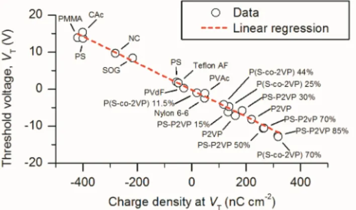
Figure 3. ‘Master’ relationship of the p branch threshold voltage to charge density. Adjusted R2: 0.967, intercept: (-0.2 ± 0.2) V, slope: (-0.036 ± 0.001) V cm2 / nC, capacitance per area: about
28 nF / cm2.
Results for the homopolymer series together with the copolymers are shown in Figure 3 (channel dimensions: 20 × 2000 μm, 230 nm oxide) where a linear relationship (adjusted R2: 0.967) is found betweenVT and the charge density. We found an intercept of (-0.2 ± 0.2) V and a
slope of (-0.036 ± 0.001) V cm2 / nC. The intercept value near 0 V emphasizes the intuitive concept that a CNN-FET enclosed in an environment free of charges should have a VT
determined by ΔΦMS, ψB and VD. Remarkably, the linear relationship obtained from a wide
variety of polymers of different chemical natures and relative permittivities indicates that a simple capacitor relationship Q = C·V with a common capacitance applies. This common
capacitance’s physical origin is still ambiguous, but it is likely related to the self-capacitance of the CNT network: The extracted capacitance per area of 28 nF / cm2 is fairly larger than the
values calculated using the parallel plate capacitor model (15 nF / cm2) and cylindrical model (~ 7 nF / cm2)29,30 (see Supp. Info. for details). The parallel plate model roughly describes the CNT network as a continuous sheet and is dependent on the dielectric’s thickness and relative
permittivity. It should be considered a limit case that appropriately approximates a CNN-FET when the CNT linear density Λ0-1 is high or when the dielectric thickness is large. The
cylindrical model is a better representation of a CNN-FET as it also takes into account the reciprocal capacitance between nanotubes. Comparison between encapsulated samples built on 90 nm and 230 nm oxide showed no measurable differences (see Figure S11, Supp. Info.). The same conclusion was drawn from samples having different thicknesses of encapsulation layer (results for PVAc are shown in Figure S13, Supp. Info.). Both results indicate that the measured charges are located near the nanotube interface or in the network. The extracted capacitance is also much lower than the self-capacitance 128 nF / cm2 of a network with a CNT linear density Λ0-1 of 3.2 µ m-1 and quantum capacitance CQ ~ 4.0 × 10⁻¹⁰ F / m.31 The lower value may also be
due to charge leakage in the interval between charging and measurement, which leads to a lower effective capacitance. However, this quoted value is for a full subband, whereas applying a gate bias equal to threshold voltage brings the Fermi level only to the band edge. We obtain a network capacitance value of ~ 30 nF / cm2 for a partially filled subband with the Fermi level 10 meV from the band edge and Λ0-1 of 3.2 µm-1. Alternatively, we hypothesize the existence of a charge
layer in proximity with the CNT layer, charges that are injected and removed upon applying an external field, and which are further localized at the very interface of the SWCNTs and the polymer, possibly because of an enhanced electric field in the proximity of nanotubes. Using the extracted capacitance value in a parallel plate capacitor model, we obtain a 95 nm distance d
with a typical relative permittivity of 3.0 (for polymer encapsulants), in stark contrast with the values computed from Cao et al.’s cylindrical model (d = 1.4 nm at Λ0-1 = 3.2 µm-1 andd = 38
nm at Λ0-1 = 10 µ m-1, RCNT = 0.65 nm, see Figure S11 and text, Supp. Info.) Although a crude
with the expected injection distance through a dielectric, but such mutual capacitors would show a dependency on the relative permittivity, which was not observed here.
The question remains as to the sign and magnitude of the charge traps for one type of polymer versus another. Significant research efforts have been put into understanding triboelectric series, and reports have correlated the charge uptake to the pKb (basicity index) of an analogue to the
polymer.26 Following the same route, we were only able to verify qualitatively this observation with our system (see Figure S14, Supp. Info.). Our observations indeed show a weak correlation of the measured charge density in this work with the triboelectric charge from Diaz et al.26 Similarly, a weak dependency could be observed with respect to the pKb and the Gutmann’s
donor number of analog molecules. Therefore, the ability of the surface to act as a base in the Lewis sense is a factor to consider when choosing an encapsulating material for SWCNT devices. Our results are in agreement with the model put forth by Fowkeset al. relating the
acid-base properties of a surface to its position on the triboelectric series.32,33
The acid-base properties can favorably be combined with the polymer hydrophobicity. We singled out P2VP as one such polymer that exhibits both basic properties and low water affinity. In P2VP, the nitrogen atom is positioned in ortho configuration and is not accessible for hydrogen bonding with water molecules. It is quite basic with a pKb of 4.98, the strongest
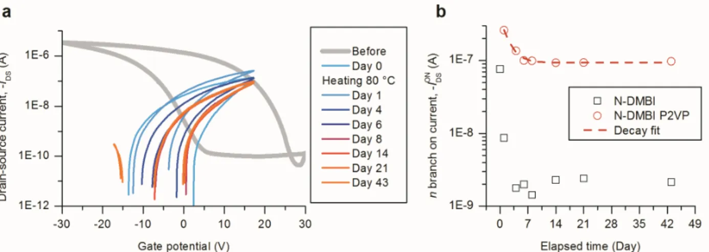
Figure 4. (a) Transfer characteristics of a CNN-FET (1000 nm oxide) doped with N-DMBI and encapsulated with a layer of P2VP spiked with N-DMBI showing the stability over time. (b) Extracted on-state current of a CNN-FET device doped with N-DMBI, but left uncapped, as compared to a device doped with DMBI but protected by a layer of P2VP containing N-DMBI, as a function of time.
By itself, P2VP encapsulation yields ambipolar transfer characteristics, at best [as seen in Figure 2(a)]. Taking advantage of its basicity and hydrophobicity, we tested the ability of P2VP, as an encapsulant, to protect n type molecular doping from oxidation. N-DMBI, an efficient
electron donor for CNT FETs,34 was dissolved in ethanol (1% w/V) and deposited by spin coating. As shown in Figure 4(a) and Figure S15 (results of the blank and unprotected devices are included in the Supp. Info.), both capped and uncapped devices with N-DMBI doped CNTs initially displayed unipolarn type behavior (channel dimensions: 40 × 1000 μm, 1000 nm oxide).
For the uncapped device however, a p branch rapidly reappeared upon interacting with oxygen
and water in air. As can be seen in Figure 4(b), the electron on-current drops hundredfold after 7 days for the unprotected devices. In contrast, devices doped with N-DMBI and protected with a capping layer (P2VP with 1% N-DMBI) showed significantly more stablen type behavior. After
extended period. Unipolar n type characteristics were indeed observed for up to 43 days of
storage in ambient, at which point a smallp branch was again observable [Figure 4(a)].
Figure 5. (a) Schematics of the diode. (b) Picture of the diode showing the partially encapsulated channel. (c) Transfer characteristics of the device prior (bare, red) and after partial encapsulation of the channel (partial, violet), and of a fully encapsulated CNN-FET (blue) for comparison. (d)
Output characteristics of the partially covered diode showing rectification. Inset: Comparison to a fully covered device on a log scale.
Stablen type CNN-FETs based on the N-DMBI and P2VP combination have been tested in the
simplest of device, a diode working on the principle of a p-n junction.35,36 Using fairly large
channels, 650 × 2000 µ m, ap-n junction was created by covering half of the channel with 0.2%
w/w DMBI and 20% w/w P2VP [Figure 5(a) and (b)]. The stripe of P2VP containing N-DMBI forms the n region of the diode while the p region forms naturally from air exposure.
Balancing of the doping of the p and n regions is crucial in the fabrication of a p-n junction
because this is how the built-in field is established. We thus adjusted the N-DMBI concentration such that the p-n junction’s maximal drain-source current would be reached close to VG = 0 V
and found 0.2% w/w to be optimal. Figure 5(c) shows the transfer characteristics of the device before encapsulation where a unipolar p type device is obtained with 5.5 µA on-state current,
5500 on / off ratio and 29.7 cm2 / V s maximum mobility. A similar device fully encapsulated with N-DMBI / P2VP displays a unipolarn type characteristic 4.2 µA on-state current, 125 on /
off ratio and 11.5 cm2 / V s maximum mobility. The two transistor types are fairly symmetric and good diode properties may be expected around VG = 0 V. As shown in Figure 5(c), the
transfer characteristic of the p-n device follows the expected dumbbell shape output for p and n
polarity transistors connected in series. The maximum current of 730 nA (negative-going sweep) close toVG ~ 0 V is also consistent with this picture. Since the device in not fully encapsulated, a
hysteresis is still present and may be more significant than for unipolar p-type transistor. Current-voltage characteristics reveal a modest level of rectification 4:1 at VG = 0 V [Figure
5(d)]. The rectification ratio improves to 8:1 when the gate potential is raised to +5 V. Breakdown is not observed within the VDS range. In comparison, the output characteristics of a
fully encapsulated n type device [Figure 5(d), inset] at VG = +5 V shows approximate ohmic
behavior. While the performance ofp-n diodes can be improved with further optimization, this
work highlights the ease of fabrication of complementary electronic elements with materials and process relevant to printing.
CONCLUSIONS
The electronic transport properties of CNN-FETs can be controlled by the choice of polymer encapsulation layer. Of note is the continuous tuning of turn-on voltage, from unipolarp type to
ambipolar transistors. Through a survey of over 20 homopolymers and copolymers, a simple relationship, the so-called “master” curve, was obtained and relates the threshold voltage VT to
the interfacial charge density present in close proximity with the carbon nanotubes. Polymer dielectric encapsulation layer thus appears as an important component of the toolbox to tune and control the electric properties of devices based on SWCNTs and other high surface area semiconducting materials.
In order to further tune the threshold voltage and achieve unipolar n type transistors, an
electron-donating molecules—prone to oxidation when left in air—was encapsulated with hydrophobic P2VP. Devices showed excellent stability for a period longer than a month. In an effort to demonstrate application to complementary electronics, we built a p-n junction that
exhibits rectification. The usefulness of polymer dielectrics really comes into force when they combine other desirable properties such as hydrophobicity and when used in conjunction with dopant molecules.
We have thus highlighted the importance of polymer dielectrics in the materials stack entering in the fabrication of SWCNT-based devices. It follows that control of the SWCNT / dielectric interface is crucial to improve the stability, operation mode and electrical characteristics of the devices, and to enable functional circuits based on complimentary logics.
METHODS
Materials: Unless noted otherwise, all materials were used as purchased. The following polymers were acquired: poly(methyl methacrylate) (medium MM, Aldrich, cat. no 18,224-9), polystyrene (MN = 45k, Aldrich, cat. no 33,165-1), poly(vinylidene difluroride) (Aldrich, cat. no
18,270-2), nylon 6-6 (Aldrich, cat. no 18,112-9), cellulose acetate (39.8 wt% acetyl content, avg.
MN = 30k (GPC), Aldrich), poly(2-vinyl pyridine) (MW 40k, cat. no 21382-10), Teflon AF
(Dupont, grade 400S2-100-1), poly(vinylidene chloride-co-methyl acrylate) (MW ~ 90k, Aldrich, cat. no 430404), poly(vinyl acetate) (MW ~ 100k, Aldrich, cat. no 189480), cellulose nitrate (collodion solution, Aldrich, cat. no 09986). The poly(styrene-co-2-vinyl pyridine) copolymers were purchased from Polymer Source Inc. with various molar fractions of styrene to 2-vinyl styrene monomers and had the following characteristics: 11.5 mol% 2VP, cat. no P7612-S2VPran, MN = 34.5k, MW = 46.5k ; 25 mol% 2VP, cat. no P7610-S2VPran, MN = 28k, MW =
38.5k ; 25 mol% 2VP, cat. no P7611-S2VPran,MN = 36.5k, MW = 47.5k ; 77 mol% 2VP, cat. no
P7616-S2VPran, MN = 28.5k,MW = 44.8k). Blends were obtained by mixing two homopolymers
(P2VP / PS) at the given weight fractions in a common solvent.
CNN-FET Fabrication: The carbon nanotube network field-effect transistors (CNN-FET) were fabricated using the following procedure: The substrates, complete with pre-existing source-drain electrodes, were purchased from the Fraunhofer Institute (Dresden). They are made of degenerately doped silicon wafers with 90 or 230 nm of thermal grown silicon dioxide with interdigitated gold electrodes deposited on top of the dielectric. The channel width was 2 mm with available channel lengths of 2.5, 5, 10 and 20 μm. Alternatively, substrates with 1000 nm thermal oxide were used. Those substrates had electrodes deposited by electron beam evaporation (Ti / Au), forming a rectangular channel 40 μm long and 1000 μm wide. Substrates
were cleaned first by ultrasonication in acetone for 5 minutes, followed by 5 minutes of ultrasound in isopropyl alcohol (IPA). Substrates were blown dry using a stream of N2, then
immediately placed in an ultraviolet (UV) / ozone cleaner for 30 minutes. Substrates were used within 20 minutes for the SWCNT deposition step. A solution of enriched semiconducting poly(9,9-di-n-dodecylfluorene) (PFDD)-wrapped carbon nanotubes37 was prepared at an
approximate concentration of 2 μg / mL in toluene from dilution of a 480 μg / mL mother solution. The diluted solution was subjected to ultrasound for 90 minutes prior to SWCNT deposition. For SWCNT deposition, the soaking method was used. Specifically, substrates were placed in a Petri dish, and then covered with the 2 μg / mL SWCNT solution. The Petri dish was covered for 16 minutes to avoid evaporation of the solvent. After this time, the substrates were soaked for 5 minutes in toluene, then 5 minutes in IPA, and finally dried by a jet of N2. The
samples were baked on a hot plate at 150 °C for 5 minutes. To complete the CNN-TFT fabrication, the edges of the substrate were gently wiped using a clean room grade swab dipped in methanol. The substrate back side was scratched using a diamond scribe and the gate electrical contact was established using copper tape (temporary) or silver lacquer (permanent).
Polymer Encapsulation: Polymer encapsulation was performed using the following procedure: CNN-FET samples were annealed at 200 °C overnight under rough vacuum and were kept on a hot plate at 150 °C prior to encapsulation. Polymer solutions were prepared in advance in an appropriate solvent and concentration. Conditions are listed for each polymer in Table S1 of the Supp. Info. The encapsulation step was carried out using spin coating, where the CNN-FET sample was briefly cooled down, set on a vacuum chuck, and then covered with the polymer solution. Spin coating proceeded in two stages, at speeds and times listed in Table S2 of the
Supp. Info. A bake, sometimes in two steps, was done afterwards to remove the residual solvent. Finally, the electrode pads were opened up using a blade manipulated under a stereomicroscope.
Generation of the ‘Master’ Relationship: A modified measurement technique was implemented that tracks the threshold voltage of a device in order to obtain the transfer characteristics with constant gate-induced charge density limits of -650 to +650 μC / m2 for all
encapsulated devices, regardless of the relative dielectric permittivity of the capping polymer. First, the effective relative dielectric permittivity of the assembly of the underlying silicon dioxide (εrsub ~ 3.9) and the capping dielectric (variable εrcap, Table S3, Supp. Info.) were
evaluated according to the relation εreff = (εrsub + εrcap) / 2. The capacitance per surface area in a
parallel plate approximation was thus estimated asCeff = ε0 εreff /d, where d is the gate dielectric
thickness. The gate-induced charge density Qind is the product of the effective surface
capacitance and the overdrive voltage (VG - VT): Qind = Ceff (VG - VT). Then, transfer
characteristics were obtained using gate potentials that are equivalent to Qind bounded by the
limits -650 and +650 μC / m2. The range of gate potentials thus becomes dependent on the threshold voltage VT of the device. First, 3 full transfer characteristics were acquired with VT
arbitrarily set to 0 V, before evaluating VT on the fly (extrapolation to IDS = 0 from a linear
regression of the p branch points above 70% of the maximum current) and adjusting the VG
limits accordingly. For every subsequent sweep, VT was reevaluated and the VG limits were
readjusted to correspond to -650 and +650 μC / m2. Because the measurement imposes a gate bias stress to the dielectric, the VT value will monotonously drift and tend to an equilibrium
value. Therefore, a total number of 16 sweeps was acquired for each device, and the last quasi equilibrium value ofVT was kept for the ‘master’ relationship.
Knowing the VT value for the encapsulated device, the measurement of the charge density at
VT was then obtained. The setup was made of a capacitive brass probe with a 2.38 mm (3/32 in)
circular cross-section held 500 µ m above the sample, which was laid on a large brass plate connected to the back gate electrode. The sample was first discharged: a grounded probe tip was connected to the drain electrode with the gate electrode also grounded and the sample was discharged for 60 seconds, at which point the grounded tip was disconnected. The probe tip was then connected to the sample’s drain electrode while biased at a potential equal to VT for 60
seconds, at which point the probe tip was disconnected while still being biased. The sample charge density was measured by moving the sample underneath the capacitive probe, while measuring the induced voltage using an electrometer, with the grounded brass plate used as a reference. The charge density was evaluated as the difference between the voltage at the grounded brass plate reference and the voltage above the encapsulated sample. This charging state corresponds to a state where the gate-induced charge densityQind is minimal because VG≈
VT, and where the measured charge density corresponds mainly to the charges at the
CNTs-polymer interface due to the chemical nature of the CNTs-polymer, that maintains a built-in potential influencingVT. Repeating this cycle of measuring the VT using the on-the-fly tracking technique
followed by a measurement of the charge density atVT for every encapsulating homopolymers, a
‘master’ relationship can be generated reflecting the built-in potential at the interface and thus yielding a predictive power to select a polymer for a desired electrical property, for instance the threshold voltage.
N type Doping: A solution of
4-(2,3-dihydro-1,3-dimethyl-1H-benzimidazol-2-yl)-N,N-dimethylbenzenamine (N-DMBI, Sigma-Aldrich) was prepared in ethanol at a concentration of 10 mg / mL. CNN-TFT samples were prepared the day before using the above procedure and
kept at 200 °C under rough vacuum until doping. Doping was performed by spin coating of the N-DMBI solution at 1000 rpm for 1 minute. A further encapsulation step was performed on one of the samples. A solution of 10 mg / mL N-DMBI in P2VP 15% w/V was prepared in chloroform. Capping was carried out using spin coating of this solution (stage 1: 9 sec at 800 rpm, stage 2: 30 sec at 3000 rpm). Then type dopant was activated by baking at 80 °C overnight
under rough vacuum.
Diode Fabrication: A solution of 0.2% w/w N-DMBI was prepared in 1-hexanol. P2VP was added to a 20% w/w concentration and stirred for 3 hours. The p-n junction was made by
covering approximately half of the channel with a stripe from this solution, using a poly(ethylene terephthalate) blade attached to a three-axis translation stage for fine control.
ASSOCIATED CONTENT
Supporting Information.
The following files are available free of charge.
Spin coating parameters, charge density measurement theory, method for the dynamic
determination of threshold voltage, results on P2VP/PS blends, capacitor models, results of the thickness series, results on charge density as a function of basicity, and supplemental results for the P(S-co-2VP) copolymer series and N-DMBIn doping experiments. (PDF)
AUTHOR INFORMATION
Corresponding Author
The manuscript was written through contributions of all authors. All authors have given approval to the final version of the manuscript.
Funding Sources
This work was funded by the National Research Council Canada through the Printable Electronics program.
Notes
Any additional relevant notes should be placed here. ACKNOWLEDGMENT
We are grateful to Patrick R. L. Malenfant for insightful discussions, and to Dan Dalacu, Joe McKee and Alexandria Snider for technical support. Ashish Sapkota acknowledges support by prof. Gyoujin Cho (Sunchon National University).
REFERENCES
(1) Lefebvre, J.; Ding, J.; Li, Z.; Finnie, P.; Lopinski, G.; Malenfant, P. R. L. High-Purity Semiconducting Single-Walled Carbon Nanotubes: A Key Enabling Material in Emerging Electronics. Acc. Chem. Res. 2017, 50 (10), 2479–2486. https://doi.org/10.1021/acs.accounts.7b00234.
(2) Qiu, S.; Wu, K.; Gao, B.; Li, L.; Jin, H.; Li, Q. Solution-Processing of High-Purity Semiconducting Single-Walled Carbon Nanotubes for Electronics Devices. Adv. Mater.
2018,1800750, 1800750. https://doi.org/10.1002/adma.201800750.
(3) Cao, Q.; Kim, H.; Pimparkar, N.; Kulkarni, J. P.; Wang, C.; Shim, M.; Roy, K.; Alam, M.; Rogers, J. Medium-Scale Carbon Nanotube Thin-Film Integrated Circuits on Flexible
Plastic Substrates. Nature 2008, 454 (7203), 495–500. https://doi.org/10.1038/nature07110.
(4) Sun, D.; Timmermans, M. Y.; Tian, Y.; Nasibulin, A. G.; Kauppinen, E. I.; Kishimoto, S.; Mizutani, T.; Ohno, Y. Flexible High-Performance Carbon Nanotube Integrated Circuits.
Nat. Nanotechnol. 2011, 6 (3), 156–161. https://doi.org/10.1038/nnano.2011.1.
(5) Artukovic, E.; Kaempgen, M.; Hecht, D. S.; Roth, S.; Grüner, G. Transparent and Flexible Carbon Nanotube Transistors. Nano Lett. 2005, 5 (4), 757–760. https://doi.org/10.1021/nl050254o.
(6) Okimoto, H.; Takenobu, T.; Yanagi, K.; Miyata, Y.; Shimotani, H.; Kataura, H.; Iwasa, Y. Tunable Carbon Nanotube Thin-Film Transistors Produced Exclusively via Inkjet Printing.Adv. Mater. 2010, 22 (36), 3981–3986. https://doi.org/10.1002/adma.201000889.
(7) Lau, P. H.; Takei, K.; Wang, C.; Ju, Y.; Kim, J.; Yu, Z.; Takahashi, T.; Cho, G.; Javey, A. Fully Printed, High Performance Carbon Nanotube Thin-Film Transistors on Flexible Substrates.Nano Lett. 2013, 13 (8), 3864–3869. https://doi.org/10.1021/nl401934a.
(8) Cao, X.; Lau, C.; Liu, Y.; Wu, F.; Gui, H.; Liu, Q.; Ma, Y.; Wan, H.; Amer, M. R.; Zhou, C. Fully Screen-Printed, Large-Area, and Flexible Active-Matrix Electrochromic Displays Using Carbon Nanotube Thin-Film Transistors. ACS Nano 2016, 10 (11), 9816–9822.
https://doi.org/10.1021/acsnano.6b05368.
(9) Chen, K.; Gao, W.; Emaminejad, S.; Kiriya, D.; Ota, H.; Nyein, H. Y. Y.; Takei, K.; Javey, A. Printed Carbon Nanotube Electronics and Sensor Systems.Adv. Mater. 2016, 28
(10) Kiriya, D.; Javey, A.; Cho, G.; Chen, K.; Yeom, C.; Yu, Z. Large-Area Compliant Tactile Sensors Using Printed Carbon Nanotube Active-Matrix Backplanes.Adv. Mater. 2015, 27
(9), 1561–1566. https://doi.org/10.1002/adma.201404850.
(11) Zhou, C.; Zhao, J.; Ye, J.; Tange, M.; Zhang, X.; Xu, W.; Zhang, K.; Okazaki, T.; Cui, Z. Printed Thin-Film Transistors and NO2 Gas Sensors Based on Sorted Semiconducting Carbon Nanotubes by Isoindigo-Based Copolymer.Carbon N. Y. 2016, 108 (2), 372–380.
https://doi.org/10.1016/j.carbon.2016.07.035.
(12) Schroeder, V.; Savagatrup, S.; He, M.; Lin, S.; Swager, T. M. Carbon Nanotube Chemical Sensors. Chem. Rev. 2019, 119 (1), 599–663. https://doi.org/10.1021/acs.chemrev.8b00340.
(13) Chortos, A.; Liu, J.; Bao, Z. Pursuing Prosthetic Electronic Skin.Nat. Mater. 2016, 15 (9),
937–950. https://doi.org/10.1038/nmat4671.
(14) Shulaker, M. M.; Hills, G.; Park, R. S.; Howe, R. T.; Saraswat, K.; Wong, P.; Mitra, S. Three-Dimensional Integration of Nanotechnologies for Computing and Data Storage on a Single Chip.Nature 2017, 547 (7661), 74–78. https://doi.org/10.1038/nature22994.
(15) Heinze, S.; Tersoff, J.; Martel, R.; Derycke, V.; Appenzeller, J.; Avouris, P. Carbon Nanotubes as Schottky Barrier Transistors.Phys. Rev. Lett. 2002, 89 (10), 106801 1-4.
(16) Cui, X.; Freitag, M.; Martel, R.; Brus, L.; Avouris, P. Controlling Energy-Level Alignments at Carbon Nanotube/Au Contacts. Nano Lett. 2003, 3 (6), 783–787.
https://doi.org/10.1021/nl034193a.
P.; Martel, R. The Role of the Oxygen/Water Redox Couple in Suppressing Electron Conduction in Field-Effect Transistors. Adv. Mater. 2009, 21 (30), 3087–3091.
https://doi.org/10.1002/adma.200900550.
(18) Schießl, S. P.; Fro, N.; Held, M.; Gannott, F.; Schweiger, M.; Forster, M.; Scherf, U.; Zaumseil, J. Polymer-Sorted Semiconducting Carbon Nanotube Networks for High-Performance Ambipolar Field-Effect Transistors. ACS Appl. Mater. Interfaces 2015, 7,
682–689. https://doi.org/10.1021/am506971b.
(19) Lee, S.-H.; Xu, Y.; Khim, D.; Park, W.-T.; Kim, D.-Y.; Noh, Y.-Y. Effect of Polymer Gate Dielectrics on Charge Transport in Carbon Nanotube Network Transistors: Low-k Insulator for Favorable Active Interface. ACS Appl. Mater. Interfaces 2016,
acsami.6b06882. https://doi.org/10.1021/acsami.6b06882.
(20) Moriyama, N.; Ohno, Y.; Kitamura, T.; Kishimoto, S.; Mizutani, T. Change in Carrier Type in High- k Gate Carbon Nanotube Field-Effect Transistors by Interface Fixed Charges. Nanotechnology 2010, 21 (16), 165201.
https://doi.org/10.1088/0957-4484/21/16/165201.
(21) Zhang, J.; Wang, C.; Fu, Y.; Che, Y.; Zhou, C. Air-Stable Conversion of Separated Carbon Nanotube Thin-Film Transistors from p-Type to n-Type Using Atomic Layer Deposition of High-κ Oxide and Its Application in CMOS Logic Circuits. ACS Nano
2011,5 (4), 3284–3292. https://doi.org/10.1021/nn2004298.
(22) Ha, T.-J. T.; Chen, K.; Chuang, S.; Yu, K. M.; Kiriya, D.; Javey, A. Highly Uniform and Stable N-Type Carbon Nanotube Transistors by Using Positively Charged Silicon Nitride Thin Films.Nano Lett. 2015, 15, 392–397.
(23) Aikawa, S.; Kim, S.; Thurakitseree, T.; Einarsson, E.; Inoue, T.; Chiashi, S.; Tsukagoshi, K.; Maruyama, S. Carrier Polarity Engineering in Carbon Nanotube Field-Effect Transistors by Induced Charges in Polymer Insulator. Appl. Phys. Lett. 2018, 112 (1),
013501. https://doi.org/10.1063/1.4994114.
(24) Ha, T. J.; Kiriya, D.; Chen, K.; Javey, A. Highly Stable Hysteresis-Free Carbon Nanotube Thin-Film Transistors by Fluorocarbon Polymer Encapsulation. ACS Appl. Mater. Interfaces 2014, 6 (11), 8441–8446. https://doi.org/10.1021/am5013326.
(25) Lefebvre, J.; Ding, J.; Li, Z.; Cheng, F.; Du, N.; Malenfant, P. R. L. Hysteresis Free Carbon Nanotube Thin Film Transistors Comprising Hydrophobic Dielectrics.Appl. Phys. Lett. 2015, 107 (24), 243301. https://doi.org/10.1063/1.4937223.
(26) Diaz, A. F.; Felix-Navarro, R. M. A Semi-Quantitative Tribo-Electric Series for Polymeric Materials: The Influence of Chemical Structure and Properties. J. Electrostat.
2004,62, 277–290.
(27) Sze, S. M.; Ng, K. K. Physics of Semiconductor Devices, 3rd editio.; John Wiley & Sons,
Inc.: Hoboken, NJ, USA, 2006. https://doi.org/10.1002/0470068329.
(28) Cao, Q.; Xia, M.; Kocabas, C.; Shim, M.; Rogers, J. A.; Rotkin, S. V. Gate Capacitance Coupling of Singled-Walled Carbon Nanotube Thin-Film Transistors. Appl. Phys. Lett.
2007,90 (2), 2005–2008. https://doi.org/10.1063/1.2431465.
(29) Schießl, S. P.; Rother, M.; Lüttgens, J.; Zaumseil, J. Extracting the Field-Effect Mobilities of Random Semiconducting Single-Walled Carbon Nanotube Networks: A Critical Comparison of Methods. Appl. Phys. Lett. 2017, 111 (19), 193301.
https://doi.org/10.1063/1.5006877.
(30) Cao, Q.; Xia, M.; Kocabas, C.; Shim, M.; Rogers, J. A.; Rotkin, S. V. Gate Capacitance Coupling of Singled-Walled Carbon Nanotube Thin-Film Transistors. Appl. Phys. Lett.
2007,90 (2), 2005–2008. https://doi.org/10.1063/1.2431465.
(31) Rosenblatt, S.; Yaish, Y.; Park, J.; Gore, J.; Sazonova, V.; McEuen, P. L. High Performance Electrolyte Gated Carbon Nanotube Transistors.Nano Lett. 2002, 2 (8), 869–
872. https://doi.org/10.1021/nl025639a.
(32) Fowkes, F. M. Quantitative Characterization of the Acid-Base Properties of Solvents, Polymers, and Inorganic Surfaces. J. Adhes. Sci. Technol. 1990, 4 (1), 669–691.
https://doi.org/10.1163/156856190X00595.
(33) Horn, R. G.; Smith, D. T.; Grabbe, A. Contact Electrification Induced by Monolayer Modification of a Surface and Relation to Acid–Base Interactions. Nature 1993, 366
(6454), 442–443. https://doi.org/10.1038/366442a0.
(34) Wang, H.; Wei, P.; Li, Y.; Han, J.; Lee, H. R.; Naab, B. D.; Liu, N.; Wang, C.; Adijanto, E.; Tee, B. C.-K.; Morishita, S.; Li, Q.; Gao, Y.; Cui, Y.; Bao, Z. Tuning the Threshold Voltage of Carbon Nanotube Transistors by N-Type Molecular Doping for Robust and Flexible Complementary Circuits. Proc. Natl. Acad. Sci. U. S. A. 2014, 111 (13), 4776–
4781. https://doi.org/10.1073/pnas.1320045111.
(35) Zhou, Y.; Gaur, A.; Hur, S. H.; Kocabas, C.; Meitl, M. A.; Shim, M.; Rogers, J. A. P-Channel, n-Channel Thin Film Transistors and p-n Diodes Based on Single Wall Carbon Nanotube Networks. Nano Lett. 2004, 4 (10), 2031–2035.
https://doi.org/10.1021/nl048905o.
(36) Biswas, C.; Lee, S. Y.; Ly, T. H.; Ghosh, A.; Dang, Q. N.; Lee, Y. H. Chemically Doped Random Network Carbon Nanotube p-n Junction Diode for Rectifier. ACS Nano 2011, 5
(12), 9817–9823. https://doi.org/10.1021/nn203391h.
(37) Ding, J.; Li, Z.; Lefebvre, J.; Cheng, F.; Dubey, G.; Zou, S.; Finnie, P.; Hrdina, A.; Scoles, L.; Lopinski, G. P.; Kingston, C. T.; Simard, B.; Malenfant, P. R. L. Enrichment of Large-Diameter Semiconducting SWCNTs by Polyfluorene Extraction for High Network Density Thin Film Transistors. Nanoscale 2014, 6 (4), 2328. https://doi.org/10.1039/c3nr05511f.