HAL Id: hal-01779823
https://hal.archives-ouvertes.fr/hal-01779823
Submitted on 27 Apr 2018
HAL is a multi-disciplinary open access
archive for the deposit and dissemination of
sci-entific research documents, whether they are
pub-lished or not. The documents may come from
teaching and research institutions in France or
abroad, or from public or private research centers.
L’archive ouverte pluridisciplinaire HAL, est
destinée au dépôt et à la diffusion de documents
scientifiques de niveau recherche, publiés ou non,
émanant des établissements d’enseignement et de
recherche français ou étrangers, des laboratoires
publics ou privés.
State Space Models for Power SiC MOSFET
Nk M’Sirdi, K Frifita, E Baghaz, A Naamane, M Boussak
To cite this version:
Nk M’Sirdi, K Frifita, E Baghaz, A Naamane, M Boussak. State Space Models for Power SiC
MOS-FET. International Conference on Electronic Engineering and Renewable Energy (ICEERE’2018),
Apr 2018, Oujda, Morocco. �hal-01779823�
State Space Models for Power SiC MOSFET
N. K. M’Sirdi, K. Frifita, E. Baghaz, A. Naamane, and M. Boussak
Aix Marseille Univ, Universite de Toulon, CNRS, LIS, Marseille, France SASV group of LIS UMR CNRS 7020, 13397, Marseille France, e-mail:
Abstract. This paper proposes a State Space Model for a power a Silicon Carbide (SiC) MOSFET. The model uses the electrical EKV MOSFET structure. The model is developed for the SiC MOSFET C2M0025120D CREE (1200V, 90A) and uses the parameters extracted from datasheet
Keywords: SiC MOSFET State Space Model, State Space Simulation Model.
1 Introduction
In high power applications, Silicon (Si) circuits are more and more replaced by SiC MOSFET devices. The wide range of operation lead to parameter variations, inherent perturbations and constraints which affect behavior of the components. Then disposal of good simulation models are necessary to get realistic simulations and accurate results.
The increasing use of switching devices in converters in power systems give more abilities but results in complex control problems related to nonlinearities involved and distortion in the electric network. Non robust controls result in a degradation of the power factor and generate voltage and current disturbances which have a different frequency than the fundamental. The state space models are helpful for systems analysis advanced controllers design. Up to now and to the best of our knowledge, the only author talking about state space representation for a MOSFET is Karvonen [1,2]. The model used, is based on SPICE® equations of discrete elements whose values are extracted from datasheet. But only the state vector is presented in the paper and in the thesis. The author uses the Modified Nodal Analysis (MNA) [3, 4]. The state space equation have never been developed for MOSFETs and proposed in literature.
In this paper, we propose state space representations, for a SiC MOSFET, deduced from a circuit model we have recently proposed [5, 6], based on the well known EKV MOSFET model [7]. The model is developed for the SiC MOSFET transistor C2M0025120D CREE (1200V, 90A) [8] and is implemented in Matlab/Simulink simulation softwares to allow easy control design for SiC MOSFET based applications. The results show that the proposed model is the most interesting to develop advanced controllers, compared to all the literature existing models.
2 N. K. M’Sirdi, K. Frifita, E. Baghaz, A. Naamane, and M. Boussak
2 SiC MOSFET Model
2.1 The Modelling Context
The MOSFET Models Several simulators have been proposed to describe the device conception and its behaviour. In [9], we find for an electro thermal simulator integrated into the environment. This is based on the use of the Verilog-A description language and the SKILL script language. The VERILOG-A language is used for modeling electrical components and for thermal modeling. Circuit design does not require all details which make such models very slow to run. The EKV model is an accurate mathematical MOSFET model developed by C. C. Enz, F. Krummenacher and E. A. Vittoz based in the 1980s, which takes into account physical properties [7].
The manufacturers propose as much as possibles models for their new circuits. Recently CREE proposed an LTspice simplified models for SiC MOSFETs like the one we are interested in [8]. The models proposed in Psim, Pspice, LMS AMESIM, Saber simulation softwares are often redundant, need solvers and complex. Linearized models are valid only in a restricted area. In order to get credible results based on simulations, we need to have accurate models, with acceptable precision.
In [1]the proposed MOSFET model is base on combined nodal and voltage loops analysis to get the equivalent circuit equations (by applying Kirchhoff’s laws) to evaluate the states and their derivatives [10]. The main contribution of [2] is the Gate-Drain capacitance characterization and its dependance on the current flow.
2.2 The nominal Electric Model
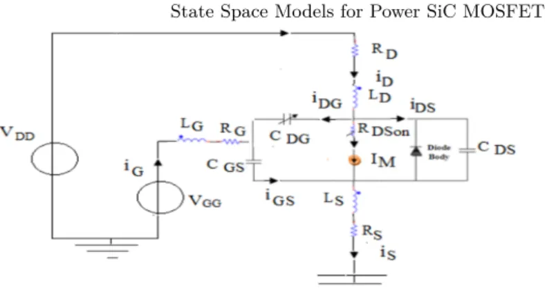
The electrical model of a SiC MOSFET proposed in [5] is based on the EKV’s one. The electric equivalent circuit of figure 1 summarizes the model description like it has been used in physical modeling based simulation softwares like Saber, Pspice and Psim. The Source, Gate and Drain voltages are respectively 𝑉𝑆, 𝑉𝐺et
𝑉𝐷 . The resistance 𝑅𝐺 estimates the gate losses as well as 𝑅𝐷 and 𝑅𝑆 are used to account for losses at the Source and Drain electrodes. The circuit includes also 3 inductors in series with the electrodes (𝐿𝐺, 𝐿𝐷, 𝐿𝑆) to describe the behavior at high frequencies.
In this model, we used parameters extracted from the data-sheet [5, 6]. The model accounts for a MOSFET operation in 3 regions. It is composed by two cur-rent sources 𝐼𝐺1 and 𝐼𝐺2. For interpolation between these 3 regions of operation, a linear combination of logarithmic functions is used by EKV. The specific current is 𝐼𝑠0 = 2.𝑉𝑡ℎ2.𝐾𝑠.𝑔𝑚. The Drain-Source current (𝐼𝐷𝑆), in the EKV MOSFET model, is defined by equation (??), as the difference between the direct 𝐼𝐺1 (2) and the reverse one 𝐼𝐺2 (3) [6].
Fig. 1. Electric model of the SiC MOSFET (C2M0080120D) 𝐼𝑀 = 𝐼𝐺1(𝑉𝑝− 𝑉𝑆) − 𝐼𝐺2(𝑉𝑝− 𝑉𝐷) (1) 𝐼𝐺1= 𝐼𝑠.𝑔𝑚. [︂ 𝐿𝑛(1 + 𝑒𝑥𝑝𝑉𝑝− 𝑉𝑠 2𝑉𝐷𝑆 ) ]︂2 (2) 𝐼𝐺2= 𝐼𝑠.𝑓 𝑡. [︂ 𝐿𝑛(1 − 𝑒𝑥𝑝𝑉𝑝− 𝑉𝐷 2 ) ]︂2 (3)
𝑔𝑚is the transconductance, 𝐾𝑠 is the slope factor, 𝑉𝑝 =(𝑉𝐺𝐾−𝑉𝑠𝑡ℎ) the pinch voltage with 𝑉𝑡ℎthe thermodynamic reference voltage and 𝑓 𝑡 the internal thermal voltage.
The following electric equations corresponding to the figure (1) can then be obtained applying the Kirchhoff laws for each current node and voltage loop of the circuit. The equation system is redundant and non linear. Let us note
𝜉𝜖 {0, 1} a state control variable introduced to switch betokening the ON/OFF
states. We have 𝜉 = 1 when the MOSFET is in ON state and respectively 𝜉 = 0 when the MOSFET is in the OFF state.
⎧ ⎪ ⎪ ⎪ ⎪ ⎪ ⎪ ⎪ ⎪ ⎪ ⎪ ⎪ ⎪ ⎪ ⎪ ⎪ ⎪ ⎪ ⎨ ⎪ ⎪ ⎪ ⎪ ⎪ ⎪ ⎪ ⎪ ⎪ ⎪ ⎪ ⎪ ⎪ ⎪ ⎪ ⎪ ⎪ ⎩ 𝑉𝐺𝐺= 𝐿𝐺𝑑𝑖𝑑𝑡𝐺 + 𝑅𝐺𝑖𝐺+ 𝑉𝐺𝑆+ 𝑉𝑆 𝑉𝐷𝐷= 𝐿𝐷𝑑𝑖𝑑𝑡𝐷 + 𝑅𝐷𝑖𝐷+ 𝑉𝐷𝑆+ 𝑉𝑆 𝑉𝐷𝐷− 𝑉𝐺𝐺= 𝐿𝐷𝑑𝑖𝑑𝑡𝐷 + 𝑅𝐷𝑖𝐷+ 𝑉𝐷𝐺− 𝐿𝐺𝑑𝑖𝑑𝑡𝐺 − 𝑅𝐺𝑖𝐺 𝑉𝑆 = 𝐿𝑆𝑑𝑖𝑑𝑡𝑆 + 𝑅𝑆𝑖𝑆 𝑉𝐷𝑆 = 𝜉.𝑅𝐷𝑆𝑜𝑛𝐼𝑀 𝑖𝐷𝑆= 𝐶𝐷𝑆𝑑𝑉𝑑𝑡𝐷𝑆 𝑖𝐺𝑆= 𝐶𝐺𝑆𝑑𝑉𝑑𝑡𝐺𝑆 𝑖𝐷𝐺= 𝐶𝐷𝐺𝑑𝑉𝑑𝑡𝐷𝐺 𝑖𝐺= 𝐶𝐺𝑆𝑑𝑉𝑑𝑡𝐺𝑆 − 𝐶𝐷𝐺𝑑𝑉𝑑𝑡𝐷𝐺 𝑖𝐷= 𝜉.𝐼𝑀+ 𝐶𝐷𝐺𝑑𝑉𝑑𝑡𝐷𝐺 + 𝐶𝐷𝑆𝑑𝑉𝑑𝑡𝐷𝑆 𝑖𝑆 = 𝜉.𝐼𝑀+ 𝐶𝐺𝑆𝑑𝑉𝑑𝑡𝐺𝑆 + 𝐶𝐷𝑆𝑑𝑉𝑑𝑡𝐷𝑆 (4)
The Modified Nodal Analysis (MNA) is in general used to solve this set of simultaneous, redundant and non linear equations [3, 4] by selecting appropriate variables. The best formulation, to avoid redundancy, computation burden and
4 N. K. M’Sirdi, K. Frifita, E. Baghaz, A. Naamane, and M. Boussak
singularities, for simulation and the control design, is the state space form, after simplifying the model.
The inputs are the voltage sources (𝑢(𝑡) = [𝑉𝐺𝐺, 𝑉𝐷𝐷]𝑇) and the outputs may be all the state variables ( 𝑖𝐺, 𝑖𝐷, 𝑖𝑆, 𝑉𝐺𝑆, 𝑉𝐷𝐺, 𝑉𝐷𝑆) or only some of them as needed by the application considered.
2.3 State Space SiC MOSFET Model
The SiC MOSFET inputs are the two voltage sources (𝑉𝐷𝐷,𝑉𝐺𝐺). The MOSFET model is in general implemented as an electric circuit (see Fig. 1) completed with an appropriate elements to switch between ON and OFF states and introducing the non linear current of equation (??) [1]. The system of equation (4) deduced by application of Kirchoff’s laws is redudant and has different time and values scales. The input, the outputs and the state equation have to be carefully selected. First State Space formulation trial The SiC MOSFET circuit is made of six energy storage elements (3 capacitances and 3 inductances). Storage elements are obviated in the system equations (4). The corresponding energy storage variables are, in nature, the internal system states (to be used for the state space representation).
We can keep as state variables the 3 currents (charging the capacitances) and the 3 voltages (inductors), which seem, a priori, independant. The chosen state vector 𝑋 is then composed by 𝑣1and 𝑣2.
𝑣1=[︀ 𝑖𝐺𝑖𝐷𝑖𝑆 ]︀𝑇 𝑎𝑛𝑑 𝑣2=[︀ 𝑉𝐺𝑆𝑉𝐷𝐺𝑉𝐷𝑆 ]︀𝑇 (5) 𝑋 =[︀ 𝑖𝐺𝑖𝐷𝑖𝑆𝑉𝐺𝑆𝑉𝐷𝐺𝑉𝐷𝑆]︀ 𝑇 (6) Let us keep only a minimum of independant equations (3 for voltages Differ-ential Equations (DAE) and 3 for currents ones):
⎧ ⎨ ⎩ 𝐿𝐺𝑑𝑖𝑑𝑡𝐺 + 𝐿𝑆𝑑𝑖𝑑𝑡𝑆 + 𝑉𝐺𝑆+ 𝑅𝐺𝑖𝐺+ 𝑅𝑆𝑖𝑆= 𝑉𝐺𝐺 𝐿𝐷𝑑𝑖𝑑𝑡𝐷 − 𝐿𝐺𝑑𝑖𝑑𝑡𝐺− 𝑅𝐺𝑖𝐺+ 𝑅𝐷𝑖𝐷+ 𝜉.𝑅𝐷𝑆𝑜𝑛𝐼𝑀− 𝑉𝐺𝑆 = 𝑉𝐷𝐷− 𝑉𝐺𝐺 𝑑𝑖𝑆 𝑑𝑡 = 𝑑𝑖𝐷 𝑑𝑡 + 𝑑𝑖𝐺 𝑑𝑡 (7) ⎧ ⎨ ⎩ −𝐶𝐷𝐺𝑑𝑉𝑑𝑡𝐷𝐺+ 𝐶𝐺𝑆𝑑𝑉𝑑𝑡𝐺𝑆 = 𝑖𝐺 𝐶𝐷𝑆𝑑𝑉𝑑𝑡𝐷𝑆 + 𝐶𝐺𝑆𝑑𝑉𝑑𝑡𝐺𝑆 = 𝑖𝑆− 𝜉.𝐼𝑀 𝑑𝑉𝐷𝑆 𝑑𝑡 − 𝑑𝑉𝐷𝐺 𝑑𝑡 − 𝑑𝑉𝐺𝑆 𝑑𝑡 = 0 (8) We get then {︃ ˙𝑣1= −𝑀1−1𝐾1𝑣1− 𝑀1−1𝐾2𝑣2+ 𝑀1−1𝑢1+ 𝜉.𝑀1−1𝑅𝐷𝑆𝑜𝑛𝑢2 ˙𝑣2= −𝑀2−1𝐾3𝑣1+ 𝑀2−1𝑢2 (9) which gives us the state space representations of the electric part of the model
˙
𝑋 = 𝐴𝑋 + 𝐵𝑢 (10)
The matrices are as follows
𝑀1= ⎡ ⎣ 𝐿𝐺 0 𝐿𝑆 −𝐿𝐺𝐿𝐷 0 −1 −1 1 ⎤ ⎦, 𝐾1= ⎡ ⎣ 𝑅𝐺 0 𝑅𝑆 −𝑅𝐺𝑅𝐷 0 0 0 0 ⎤ ⎦ (11) 𝐾2= ⎡ ⎣ 1 0 0 −1 0 0 0 0 0 ⎤ ⎦ 𝑎𝑛𝑑 𝑢1= ⎡ ⎣ 𝑉𝐺𝐺 𝑉𝐷𝐷− 𝑉𝐺𝐺 0 ⎤ ⎦ (12) and 𝑀2= ⎡ ⎣ 𝐶𝐺𝑆 −𝐶𝐷𝐺 0 𝐶𝐺𝑆 0 𝐶𝐷𝑆 −1 −1 1 ⎤ ⎦ 𝑎𝑛𝑑 𝑢2= ⎡ ⎣ 0 −𝐼𝑀 0 ⎤ ⎦ (13) 𝐾3= ⎡ ⎣ −1 0 0 0 0 −1 0 0 0 ⎤ ⎦ (14)
Computing the inverse matrices 𝑀1−1et 𝑀2−1, we get the A matrix
𝐴 = ⎡ ⎢ ⎢ ⎢ ⎢ ⎢ ⎢ ⎣ −𝑅𝐺(𝐿𝐷+𝐿𝑆) 𝑑1 𝑅𝐷𝐿𝑆 𝑑1 −𝑅𝑆𝐿𝐷 𝑑1 −𝐿𝐷−𝐿𝑆 𝑑1 0 0 𝑅𝐺𝐿𝑆 𝑑1 −𝑅𝐷(𝐿𝐺+𝐿𝑆) 𝑑1 −𝐿𝐺𝑅𝑆 𝑑1 𝐿𝑆 𝑑1 0 0 −𝑅𝐺𝐿𝐷 𝑑1 −𝑅𝐷𝐿𝐺 𝑑1 −𝑅𝑆(𝐿𝐷+𝐿𝐺) 𝑑1 −𝐿𝐷 𝑑1 0 0 𝐶𝐷𝑆 𝑑2 0 𝐶𝐷𝐺 𝑑2 0 0 0 −(𝐶𝐷𝑆+𝐶𝐺𝑆) 𝑑2 0 𝐶𝐺𝑆 𝑑2 0 0 0 −𝐶𝐺𝑆 𝑑2 0 𝐶𝐷𝐺+𝐶𝐺𝑆 𝑑2 0 0 0 ⎤ ⎥ ⎥ ⎥ ⎥ ⎥ ⎥ ⎦ (15)
This state space representation offers a very bad numerical conditionning. We can remark that we have two null eigen values 𝜆1 = 𝜆2 = 0. This means
that there are two integrators in the process. This will integrate twice all the numerical computation errors. There are two big complex conjugate eigen values, in the A matrix which are for our case: 𝜆3= 𝜆*34= −1.1250𝑒 + 08 + 1.0468𝑒 + 08𝑖.
The last two eigen values are the bigest and the smallest ones 𝜆5= −87.903𝑒 + 06
and 𝜆6= 8.4371𝑒 − 09. They have as ratio 𝜆𝜆12 = −1.0419𝑒 + 16 which show us
that this matrix is very badly conditionned for simulation omputings.
This proves that this state space form cannot be used in simulations because of the numerical problems; this justifies the need of the NDA approach [1]. Second State Space formulation The fact we got two zero eigen values means that special relations exist between the state variables considered and inputs. Effectively we can remark that in the system equations we have Algebraic equations mixed with differential equations. The previous system 4 can then be rewretten to emphasize the Differential and Algebraic Equations (DAE). We can observe, in the oridnary differential equations (ODEs) of 16 and 17, that
6 N. K. M’Sirdi, K. Frifita, E. Baghaz, A. Naamane, and M. Boussak
dependence of the three currents and the three voltages is obvious. Each one of those systems has then only 2 independent ODEs, as their third one expresses only the difference beetwen the previous ones.
⎧ ⎨ ⎩ 𝐿𝐺𝑑𝑖𝑑𝑡𝐺 + 𝐿𝑆𝑑𝑖𝑑𝑡𝑆 + 𝑅𝐺𝑖𝐺+ 𝑅𝑆𝑖𝑆+ 𝑉𝐺𝑆= 𝑉𝐺𝐺 𝐿𝐷𝑑𝑖𝑑𝑡𝐷 + 𝑅𝐷𝑖𝐷+ 𝑉𝐷𝑆+ 𝐿𝑆𝑑𝑖𝑑𝑡𝑆 + 𝑅𝑆𝑖𝑆= 𝑉𝐷𝐷 𝑖𝐷= 𝑖𝑆− 𝑖𝐺= 𝑖𝐷𝐺+ 𝑖𝐷𝑆+ 𝜉.𝐼𝑀 (16) ⎧ ⎨ ⎩ −𝐶𝐷𝐺𝑑𝑉𝐷𝐺 𝑑𝑡 + 𝐶𝐺𝑆 𝑑𝑉𝐺𝑆 𝑑𝑡 = 𝑖𝐺 𝐶𝐷𝑆𝑑𝑉𝑑𝑡𝐷𝑆 + 𝐶𝐺𝑆𝑑𝑉𝑑𝑡𝐺𝑆 = 𝑖𝑆− 𝜉.𝐼𝑀 𝑉𝐷𝑆 = 𝑉𝐷𝐺+ 𝑉𝐺𝑆 (17)
So we can remark that the variables 𝑖𝐷 and 𝑉𝐷𝑆 (respectively) can be deduced by algebraic equations from the state variables 𝑣1 = [︀𝑖𝐺, 𝑖𝑆]︀
𝑇 and
𝑣2=[︀ 𝑉𝐺𝑆, 𝑉𝐷𝐺 ]︀𝑇
(respectively). In addition these equations include the system non linearities and thermal dependances and variations. We can replace 𝑖𝐷=
𝑖𝑆−𝑖𝐺 = 𝑖𝐷𝐺+𝑖𝐷𝑆+𝐼𝑀. The same can be done for the voltage 𝑉𝐷𝑆 = 𝑉𝐷𝐺+𝑉𝐺𝑆 which imposes the inherent EKV current sources. Then we get the following ODE systems become {︂ 𝐿𝐺𝑑𝑖𝑑𝑡𝐺 + 𝐿𝑆𝑑𝑖𝑑𝑡𝑆 + 𝑅𝐺𝑖𝐺+ 𝑅𝑆𝑖𝑆+ 𝑉𝐺𝑆= 𝑉𝐺𝐺 −𝐿𝐷𝑑𝑖𝐺 𝑑𝑡 + (𝐿𝐷+ 𝐿𝑆) 𝑑𝑖𝑆 𝑑𝑡 − 𝑅𝐷𝑖𝐺+ (𝑅𝐷+ 𝑅𝑆) 𝑖𝑆+ 𝜉.𝑅𝐷𝑆𝑜𝑛𝐼𝑀 = 𝑉𝐷𝐷 (18) {︂ 𝐶𝐺𝑆𝑑𝑉𝑑𝑡𝐺𝑆 − 𝐶𝐷𝐺𝑑𝑉𝑑𝑡𝐷𝐺− 𝑖𝐺= 0 (𝐶𝐺𝑆+ 𝐶𝐷𝑆)𝑑𝑉𝐺𝑆 𝑑𝑡 + 𝐶𝐷𝑆 𝑑𝑉𝐷𝐺 𝑑𝑡 − 𝑖𝑆 = −𝜉.𝐼𝑀 (19) Finally {︃ ˙𝑣1= −𝑀1−1𝐾1𝑣1− 𝑀1−1𝐾2𝑣2+ 𝑀1−1𝑢1 ˙𝑣2= −𝑀2−1𝐾3𝑣1+ 𝜉.𝑀2−1𝑢2 (20) The matrices are as follows
𝑀1= [︂ 𝐿𝐺 𝐿𝑆 −𝐿𝐷𝐿𝐷+ 𝐿𝑆 ]︂ , 𝐾1= [︂ 𝑅𝐺 𝑅𝑆 −𝑅𝐷𝑅𝐷+ 𝑅𝑆 ]︂ (21) 𝐾2= [︂ 1 0 0 0 ]︂ 𝑎𝑛𝑑 𝑢1= [︂ 𝑉𝐺𝐺 𝑉𝐷𝐷 ]︂ (22) and 𝑀2= [︂ 𝐶𝐺𝑆 −𝐶𝐷𝐺 𝐶𝐺𝑆+ 𝐶𝐷𝑆 𝐶𝐷𝑆 ]︂ 𝑎𝑛𝑑 𝑢2= [︂ 0 −𝐼𝑀 ]︂ (23) 𝐾3= [︂ −1 0 0 −1 ]︂ (24) The matrices determinants are 𝑑1 = 2.7900.10−16 and 𝑑2 = 2.1135.10−19
two equations separately (one for 𝑣1 and the second for 𝑣2). The system has as
eigen values 𝜆𝑝:
𝜆𝑝= 108[−0.4679 + 6.3800𝑖; −0.4679 − 6.3800𝑖; −1.0967 + 1.7151𝑖; −1.0967 − 1.7151𝑖] (25)
3 Simulations Tests and Model Validation
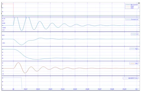
In order to verify the afore-mentioned characteristics, a series of simulation circuits were developed. The developed model has been implemented in Saber, Pspice and Psim softwares and compared to the experimental curves presented by the SiC MOSFET data sheet for its validation and parameters extraction.
Fig. 2. Transeint responses
4 Conclusion
A new state space model has been proposed in this paper for a SiC Power MOS-FET. It is deduced from an electric equivalent circuit, by selecting appropriate nonlinear differential equations written in a state space form.
This model can be implemented under Matlab/Simulink software and tested in simulation. The Characteristics of the MOSFET simulation models (on-state resistance, threshold voltage, and transconductance, etc...) are compared to Pspice simulation model
The simulation model of SiC power MOSFET is easy to use in numerical design and prototyping of electric circuits and simulations. The future work of our staff will be on nonlinear and robust control of a power circuit including the SiC MOSFETs.
8 N. K. M’Sirdi, K. Frifita, E. Baghaz, A. Naamane, and M. Boussak
Acknowledgments This research activity was held by the SASV group of the LIS and co funded by an FUI project. The authors would like to thanks also Europractice (http://www.europractice.stfc.ac.uk/ ).
References
1. A. Karvonen and T. Thiringer, “Mosfet modeling adapted for switched applications using a state-space approach and internal capacitance characterization,” in
Inter-national Conference on Power Electronics and Drive Systems (PEDS) pp1107 - 1112 Taipei, Taiwan 2-5 Nov. 2009, 2009. 1, 2.1, 2.3, 2.3
2. A. Karvonen, “Emi from switched converters : Simulation methods and reduction techniques,” Chalmers University, Licentiate Thesis at Department of Energy and Environment, Division of Electric Power Engineering; Chalmers University of Technology Goteborg, Sweden 2011, Goteborg, Sweden, 2009. 1, 2.1
3. H. Chung-Wen, A. Ruehli, and P. Brennan, “The modified nodal approach to network analysis,”IEEE Transactions on Circuits and Systems, vol. 22, no. 6, pp. 504–509, 1975. 1, 2.2
4. L. M. Wedepohl and L. Jackson, “Modified nodal analysis: an essential addition to electrical circuit theory and analysis,”Journal of Engineering Science and Education, vol. 11, no. 3, pp. 84–92, 2002. 1, 2.2
5. N. K. M’Sirdi, E. Baghaz, K. Frifita, A. Naamane, and M. BOUSSAK, “Simulation model of a sic power mosfet variables estimations and control of a power source,” in
14th International Conference on Informatics in Control, Automation and Robotics - Volume 1: ICINCO, O. G. 1 and K. Madani, Eds., vol. 1, july 2017, pp. 637–643.
1, 2.2, 2.2
6. K. Frifita, N. K. M’Sirdi, E. Baghaz, A. Naamane, and M. Boussak, “Electro-thermal model of a silicon carbide power mosfet,” submitted to ICEERE2018, Saidia Oujda Morroco, April 2018. 1, 2.2
7. E. Vittoz, C. C. Enz, and F. Krummenacher, “A thermal characterization of power transistors semiconductor,” vol. 11. 1, 2.1
8. CREE, “Sic power mosfet cmf20120d datas-sheet and application note,”http://www.
cree. com/products/pdf/CMF20120D. pdf, 2015. 1, 2.1
9. A. Maxim and G. Maxim, “A high accuracy power MOSFET SPICE behavioral macromodel including the device selfheating and safe operating area simulation.” 2.1
10. G. Verneau, L. Aubard, J. Crébier, and J. Schanen, “Empirical power mosfet modeling: Practical characterization and simulation implantation,” in37th IAS
Annual Meeting. Conference Record of theVolume4, . t. I. A. M. ConferenceIndustry
Applications Conference, Ed., vol. 4, no. DOI10.1109/IAS.2002.1042785. IAS Annual Meeting (IEEE Industry Applications Society) 4:2425 - 2432, February 2002, pp. 2425–2432. 2.1