HAL Id: hal-01986953
https://hal-amu.archives-ouvertes.fr/hal-01986953
Submitted on 19 Jan 2019
HAL is a multi-disciplinary open access
archive for the deposit and dissemination of
sci-entific research documents, whether they are
pub-lished or not. The documents may come from
teaching and research institutions in France or
abroad, or from public or private research centers.
L’archive ouverte pluridisciplinaire HAL, est
destinée au dépôt et à la diffusion de documents
scientifiques de niveau recherche, publiés ou non,
émanant des établissements d’enseignement et de
recherche français ou étrangers, des laboratoires
publics ou privés.
Distributed under a Creative Commons Attribution| 4.0 International License
Design and realization of light absorbers using
plasmonic nanoparticles
Ludovic Escoubas, Miriam Carlberg, Judikaël Le Rouzo, Florent Pourcin,
Jörg Ackermann, Olivier Margeat, Clement Reynaud, David Duche,
Jean-Jacques Simon, Rose-Marie Sauvage, et al.
To cite this version:
Ludovic Escoubas, Miriam Carlberg, Judikaël Le Rouzo, Florent Pourcin, Jörg Ackermann, et al..
Design and realization of light absorbers using plasmonic nanoparticles. Progress in Quantum
Elec-tronics, Elsevier, 2019, �10.1016/j.pquantelec.2018.12.001�. �hal-01986953�
UNCORRECTED
PROOF
Ludovic Escoubas
a, ∗, Miriam Carlberg
a, Judikael Le Rouzo
a, Florent Pourcin
b, Jorg Ackermann
b,
Olivier Margeat
b, Clement Reynaud
a, David Duche
a, Jean-Jacques Simon
a, Rose-Marie Sauvage
c,
Gérard Berginc
daAix Marseille Univ, Université de Toulon, CNRS, IM2NP, Marseille, France bAix Marseille Univ, CNRS, CINAM, Marseille, France
cDGA/DS/MRIS, 75015, Paris, France dThales Optronics, 78990, Elancourt, France
A R T I C L E I N F O A B S T R A C T
The applications of light absorbers concern photodetectors, optical filters, solar applications or flexible electronics. In this review, we will detail the application of such light absorbers and we will develop the main demonstrations of the use of metallic nanoparticles embedded within a host matrix to fabricate coatings aiming at harvesting light. We will explain how chemically syn-thetized silver nanoparticles of various shapes (spheres, cubes, …) and sizes allow controlling the optical properties of heterogeneous thin film layers. By coupling the optical characterizations with computer modeling, we will describe how the nanoparticles behave both individually and collectively. To control reflected and absorbed light by thin film layers containing nanoparticles several points have to be addressed: the relation between the shape of the nanoparticle and the absorptance of the layer, the interaction of light between nanoparticles and the collective behav-ior of aggregates.
1. Introduction
Many applications require having at disposal or designing materials, which are able to absorb the light, either specifically for some light incidences and spectral ranges chosen by users, or in broad-ranges of incidences and wavelengths. In most appli-cations the efficiency of absorption must be maximal and must be obtained with the thinnest materials, very often in thin lay-ers, and with the wish that these thin layers perfectly fit with the forms of the surfaces they cover. When one wishes to go be-yond the absorption ranges usually found in the materials in their natural state, one possibility is to design new synthetic mate-rials made of alloys of constituents, which are often of complex structures. The structuring of these matemate-rials, when the charac-teristic dimensions are close to the wavelengths to be absorbed, greatly influences the properties of absorption in terms of spec-tral range, of angular fields and of efficiency. To build such thin materials, which are ultra-absorbing and not available in nat-ural state, resonance phenomena of light found in Fabry-Perot cavities or plasmonic effects are very useful. These plasmonic ef-fects may appear in the gap between two thin metallic layers, and are called gap plasmons, or on the surface of structured materi-als (called surface plasmons), or even directly at the level of nanoparticles of metal or degenerate semiconductor (called localized plasmons). Thus, it is possible to obtain very strong light absorption with very small amount of material. Furthermore, associat
∗Corresponding author.
Email address: [email protected] (L. Escoubas)
https://doi.org/10.1016/j.pquantelec.2018.12.001 Available online xxx
UNCORRECTED
PROOF
L. Escoubas et al. Progress in Quantum Electronics xxx (2019) xxx-xxx
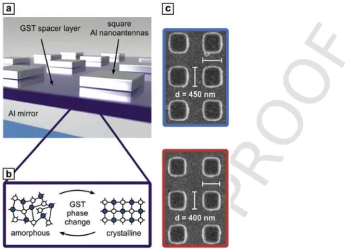
Fig. 1. a) Sketch of a switchable perfect absorber device. Arrays of square aluminum (Al) nanoantennas are stacked above a spacer layer of the phase change material GST-326 and an Al mirror. b) Amorphous to crystalline phase transition in GST. c) SEM images of two representative perfect absorber devices fabricated with antenna side lengths of d=400nm and d=450nm @Wiley (extracted with permission from ref 7 - https://doi.org/10.1002/adma.201502023).
Fig. 2. (a) Schematic of the dual-band perfect absorber structure and the incident polarization configuration. (b) A SEM image of the designed structure. @OSA (ex-tracted with permission from ref 8 - https://doi.org/10.1364/OE.19.015221).
Fig. 3. Photograph of resonant color filters. @ACS Publications (extracted with permission from ref 10 - https://doi.org/10.1021/ph500410u).
ing optical resonators, whose dimensions are close to the wavelength, allows electromagnetic interactions to be obtained, which opens new possibilities of controlling the light propagation in the materials.
The aim of this article is firstly to describe the general working principles of light absorbers based on plasmonic effect, mainly obtained from nanoparticles. In a second step, we discuss the synthesis routes of plasmonic nanoparticles and we show
UNCORRECTED
PROOF
localized between the base of the silver nanocubes and the gold surface.
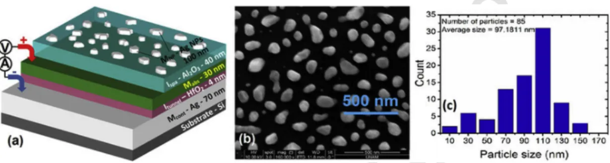
Fig. 5. Schematic of a double-stacked MIM (i.e. MIMIM) photodetectors operating in the near-infrared (NIR) spectrum up to 1200nm wavelength and presented in ref 17. The MIMIM comprised of metal nanoparticles (MNP), spacer insulator (Ispa), absorbing metal (Mabs), tunneling insulator (Itunnel) and bottom contact metal (Mcont), (b) SEM image of the nanoparticles after annealing 10nm Silver film for 20minat 500°C and (c) the size distribution of particles from SEM image of part (b) @Nature (extracted with permission from Ref. [17] - https://doi.org/10.1038/srep42349).
Fig. 6. a) Specular measured and Transfer Matrix Method (TMM) computed reflectances of Ag nanocubes:PVP composite layer deposited on Si* (b) TEM picture of silver nanocubes embedded in PVP c) Optical photograph of the Ag nanocubes:PVP composite on glass substrates.
how it is possible to control their shapes, which can be spherical, prismatic or cubic for example, and thus affecting the inter-actions with the light. Then, we present analytical and numerical methods to model the interinter-actions between these nanoparticles and the light waves: Mie theory, Discrete Dipole Approximation (DDA), Finite Difference Time Domain (FDTD). The modeling of the light propagation in these complex environments including nanoparticles of various forms requires the measurement of the optical complex indices in order to implement them in the computation codes. So, we will explain how spectroscopic ellipsom-etry measurement associated with Cauchy, Gaussian, or Lorentz models and the theory of effective medium allow extracting the values of the optical complex indices of these composite materials. Finally, we will devote the last part of the article to present achievements in which the light interactions between nanoparticles is exploited in very specific configurations: dimers consisting
UNCORRECTED
PROOF
L. Escoubas et al. Progress in Quantum Electronics xxx (2019) xxx-xxx
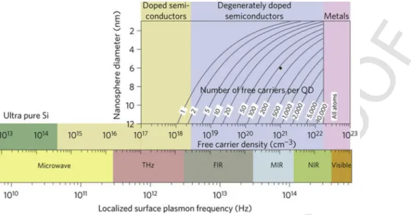
Fig. 7. Localized surface plasmon resonance (LSPR) frequency dependence on free carrier density and doping constraints @Nature (extracted with permission from ref 30 - https://doi.org/10.1038/nmat3004).
Fig. 8. Seed and nanoparticle growth process.
of two nanoparticles interacting in the Kerker's conditions or aggregates of particles (dimers, trimers, multimeres), whose 3D geome-try is perfectly controlled to create spectral absorption bands on the demand.
2. Design of plasmonic light absorbers
By definition, a light absorber is a device, whose optical properties are controlled. The specular and the diffuse reflectance, and also the amount of light transmitted through, are minimized. The device absorbs the incident light at a particular wavelength or a broad wavelength domain, ranging from the optical to the longest wavelength domain, and within the broadest solid angle for both linear s and p polarization states. Such absorbers are of interest for many applications, depending on their optical properties, as will be discussed in the following. Because of the large number of applications, extensive research has been done in order to define the optimal design of a light absorber.
2.1. Metal insulator metal (MIM) structure
A first highly-efficient absorber design concerns the metal-insulator-metal (MIM) structures [1–3]. The simplest MIM structure is composed of two metallic layers separated by a dielectric layer. The bottom layer is thick to act as a reflector and avoid opti-cal transmission. A simple MIM structure presents a single absorption band because there is a single resonant mode within the di-electric cavity. The incident light is trapped inside the cavity. The position of the absorption band depends on the chosen metal and dielectric materials. A typical choice for the metallic layer, in order for the device to absorb the light in the visible wave-length band, is silver or gold. Typical dielectric spacers are Si, SiO2, AlO3or TiO2. Depending on the aimed absorption band
UNCORRECTED
PROOF
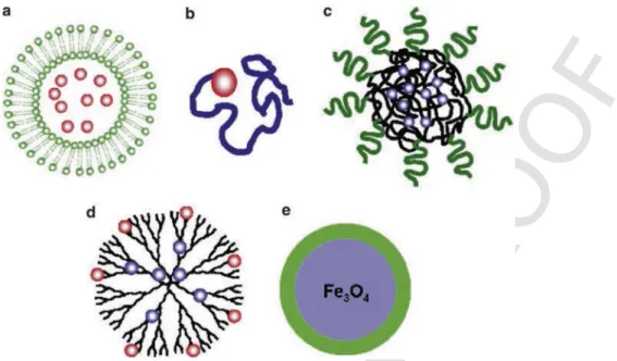
Fig. 9. Schematic illustration of therapeutic nanoparticle platforms in preclinical development: (a) liposome, (b) polymer–drug conjugate, (c) polymeric nanoparticle, (d) dendrimer, and (e) iron oxide nanoparticle. The red dots represent hydrophilic drugs and the blue dots represent hydrophobic drugs @Nature Publishing Group (extracted with permission from ref 62 - https://doi.org/10.1038/sj.clpt.6100400).
Fig. 10. (a) Non uniform mesh and (b) TFSF disposition in the simulation window.
and applications, the suited materials and their thicknesses can be determined by computer simulations, such as finite difference time domain (FDTD) method, and numerical calculations, such as transfer matrix method (TMM) [1,4].
In order to absorb the light on a broader wavelength range, the number of layers can be increased to create multilayered MIM. Each dielectric cavity will be excited by a different wavelength of the incident light and therefore increase the absorption band of the device. Recent reports show up to 90% absorption from 400 to 1640nm for multilayered thin film stacks [4]. The advantages of multilayered MIM structures are undeniable, but the fabrication methods are an important factor in their industrial utilizations.
Deposition techniques such as sputtering [3] or thermal evaporation, sol-gel/spin coating [1] or Langmuir-Blodgett [5] methods, are of particular interest because of their simplicity and potential for low cost upscaling. Recent works have reported their ability to achieve efficient absorbers for large angles of incidence with a low polarization sensitivity.
Broadband multilayered MIM structure absorbers find applications in thermo and photovoltaic solar cells [6], radar technologies and thermal imaging [7] (see Fig. 1).
Experimental measurements show that the design of Fig. 1a exhibits low reflectance and hence very high resonant absorption (A>90%) in the MWIR spectral range. Geometrical tunability of the resonance wavelength is achieved by varying the side length d of the resonant square Al nanoantennas, with larger antennas corresponding to higher resonance wavelengths. When heating the sample above the germanium antimony telluride (GST) crystallization temperature, the resonance undergoes a pronounced phase-change-in-duced spectral redshift of up to 0.7μm while maintaining high absorbance.
Another absorption mechanism used in MIM structures is based on plasmon resonances [8,9]. The incident electromagnetic wave is coupled into the resonant dielectric gap in the form of a gap-plasmon and at the metal interface in the form of a surface-plasmon. Either the upper or the bottom metallic layer is structured to take advantage of the surface plasmon resonances.
UNCORRECTED
PROOF
L. Escoubas et al. Progress in Quantum Electronics xxx (2019) xxx-xxx
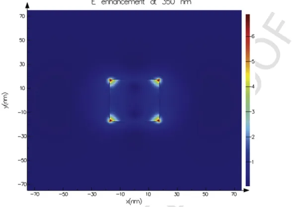
Fig. 11. Example of the FDTD computed amplitude of the electric field enhancement on a 35nm edge size silver cube in a PVP polymer matrix at λ=350nm.
Fig. 12. Example of coupled resonance calculated by FDTD: electric field enhancement at the dipolar resonance wavelength of silver nanoprisms displayed in a periodic squared pattern. The electromagnetic wave is travelling along x.
As shown in Fig. 2, the structure is made from a film stack comprising:
- a top metal layer composed of an elliptical gold nanodisk array, which geometrical parameters such as a, b and d can be tuned individually to control the interaction with light.
- a spacing dielectric SiO2, MgF2, or polymer layer with low permittivity to reach high absorption. The thickness of the dielectric layer
is of high importance as it influences the dipole resonance. By increasing the thickness, the resonance effect diminishes and the overall
UNCORRECTED
PROOF
Fig. 13. Simplified spectroscopic ellipsometry measurement setup.
Fig. 14. Effective medium approach. Table 1
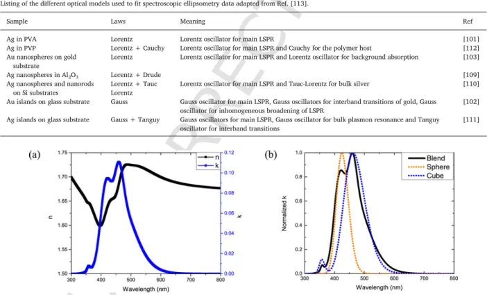
Listing of the different optical models used to fit spectroscopic ellipsometry data adapted from Ref. [113].
Sample Laws Meaning Ref
Ag in PVA Lorentz Lorentz oscillator for main LSPR [101]
Ag in PVP Lorentz + Cauchy Lorentz oscillator for main LSPR and Cauchy for the polymer host [112] Au nanospheres on gold
substrate Lorentz Lorentz oscillator for main LSPR and Lorentz oscillator for background absorption [103]
Ag nanospheres in Al2O3 Lorentz + Drude [109]
Ag nanospheres and nanorods
on Si substrates Lorentz + TaucLorentz Lorentz oscillator for main LSPR and Tauc-Lorentz for bulk silver [110] Au islands on glass substrate Gauss Gauss oscillator for main LSPR, Gauss oscillators for interband transitions of gold, Gauss
oscillator for inhomogeneous broadening of LSPR [102]
Ag islands on glass substrate Gauss + Tanguy Gauss oscillators for main LSPR, Gauss oscillator for bulk plasmon resonance and Tanguy
oscillator for interband transitions [111]
Fig. 15. (a) Complex refractive indices n and k of nanospheres and nanocubes blend in PVP and (b) the normalized extinction coefficient k compared to the one of nanospheres in PVP and nanocubes in PVP. @OSA (extracted with permission from Ref. [116]).
UNCORRECTED
PROOF
L. Escoubas et al. Progress in Quantum Electronics xxx (2019) xxx-xxx
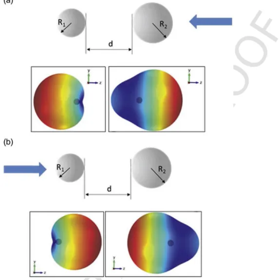
Fig. 16. Scheme of the considered geometry. The system is composed of two silicon nanoparticles located at a distance d between them. The particle sizes are such that, while one nanoparticle has zero backscattering, the other one satisfied the MF scattering at the same incident wavelength (λ=700nm). The bottom figures show the 3-D spatial distribution of the light scattering of each isolated nanoparticle, with blue being the lowest intensity and red being the highest intensity. Depending on the incident direction, from right to the left (a) or vice versa (b), the light concentration on the gap drastically changes. @IEEE Photonics Society (extracted with permission from Ref. [123] - https://doi.org/10.1109/JPHOT.2016.2577714).
- a bottom gold layer deposited on top of the substrate
Fig. 2 (b) shows a SEM top-view image of the structure. Contrary to the component shown in Fig. 2, devices are generally highly polarization dependent and the absorption band is narrow, which makes them promising candidates for sensing applications, col-ored-optical filters [10] (see Fig. 3) and polarization detectors [11].
As shown in Fig. 3, resonant optical filters can be fabricated from modified, asymmetric metal–insulator–metal (MIM) based Fabry–Perot cavities including plasmonic, lossy ultrathin (∼30nm) metallic films used as the top metallic layer. Different colors can be obtained by controlling the dielectric spacer thickness.
Because they can be confined over nanometric areas at dielectric-metal interfaces or into nanocavities, surface plasmons can create very high electric fields. This feature makes them particularly interesting for optical rectification purposes. One of the promises of optical rectification is to enable the fabrication of devices that convert light into electricity without relying on the photovoltaic effect. As a consequence, such a device – referred as optical rectennas (rectifying antenna) - would not be subject to the so-called Schockley Queisser limit that bounds the efficiencies of PV solar cells to 33% for single junctions. The concept of optical rectennas goes back to the 70's when Bailey [12] proposed that a nanoscale antenna coupled with a rectifier could har-vest electromagnetic waves in the visible and infrared region. Recent work have already demonstrated power production origi-nating from optical rectennas [13], but research in this field remains at stage of proof of concept. We have assembled very re-cently rectennas solar cells composed of plasmonic nanocubes (see Fig. 4a) associated with rectifying self-assembled molecular diodes that allow a plasmon cavity mode coupling between silver nanocubes and a gold plane. Thus, an electric field enhance
UNCORRECTED
PROOF
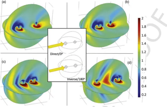
Fig. 17. Distribution of the electric field in the incident and orthogonal planes (including the middle point of the gap) in the region between the nanoparticles consid-ering an incident beam of (λ=700nm). The geometry and view are shown in the center. (a) and (b) corresponding to the configuration of Fig. 16a with gap distances of d=375nm and d=200nm, respectively. (c) and (d) corresponding to the configuration of Fig. 16b with gap distances of d=120nm and d=445nm, respectively. @IEEE Photonics Society (extracted with permission from Ref. [123]- https://doi.org/10.1109/JPHOT.2016.2577714).
ment up to two orders of magnitude (intensity enhancement up to four orders of magnitude) is obtained that could enable the rectifi-cation process without any applied bias. The nanocubes shown in Fig. 4 are self-assembled thanks to dithiol molecules. By choosing a given molecule length, the gap thickness below the cube is controlled within a nanometer accuracy. A holed polymer matrix controls the periodicity of the nanocubes array (see Fig. 4b), which has a crucial role in the optical absorption by the device.
2.2. Plasmonic nanoparticles light absorbers
Plasmonic nanoparticles display localized surface plasmon resonances [14,15] (LSPRs), which induce a selective light absorption and scattering depending on the material, size, shape and environment of the nanoparticle. Indeed, LSPRs excited in metallic nanopar-ticles are non-propagating plasmon excitations. Since the size of a metallic nanoparticle is on the same scale of the penetration depth of electromagnetic waves in metals (e.g., 20∼30nm for Ag and Au), the external field can penetrate the whole particle and shift the conduction electrons with respect to the rigid ion lattice. Thus, the charges are separated and this charge separation results in a restoring force and then an oscillation. The oscillation frequency is mainly related to effective electron mass, charge density, and geometry of the particle, as well as the properties of the surrounding medium. The amplitude of the induced electromagnetic field is much stronger than exciting fields (over 10 times). A comprehensive review on the applications of plasmonic effects to solar cells has been published by Atwater and Polman [16].
The nanoparticles can be:
- either deposited directly onto a thin dielectric spacer on a metallic substrate to fabricate a resonant absorbing MIM structure and the light is then absorbed through surface plasmon resonances [17] (see Fig. 5) in the cavity between the metal layer and the nanopar-ticles. The optical response of the deposited metasurfaces relies on the spacing and the nanocrystal size as well as nanoparticle density. This allows a large parameter space to fine tune the optical response [18,19]. It is essential here to carefully choose the underlying metal substrate as well as the thickness of the dielectric spacer to enhance optical couplings [20–22].
- or embedded within a host matrix. In this second configuration, the light is absorbed by the localized surface plasmon reso-nances of the nanoparticles inside the composite layer and the absorbed light can be locally converted in to heat [23]. The op-tical properties of the light absorber are mainly controlled by the size, density and shape of the nanoparticles and are indepen-dent of the choice of the substrate [24]. The role of the host materials, usually a transparent polymer, is to facilitate processing of homogeneous films over large areas and to control spacing and organization of the plasmonic absorber inside the nanocom-posite with dedicated optical properties. For example, Fig. 6a shows the specular reflectance spectra of a PVP layer with em-bedded Ag nanocubes. Deposited on Si, those nanocomposite layers produce a strong reflectance dip over the range of absorp
UNCORRECTED
PROOF
L. Escoubas et al. Progress in Quantum Electronics xxx (2019) xxx-xxx
Fig. 18. (A–C) Schematic and SEM images of nanocube assembly observed at embedding depths of 15nm, 42nm and 61nm of NCo. Scale bar=500nm. (D–F) Corre-sponding statistical analysis showing the population distributions of monomers, dimers, trimers, and multimers in each assembly. (G–I) CorreCorre-sponding optical extinction spectra taken an incident illumination with a broadband white light source. The extinction spectrum of as-deposited NCo nanocubes prior to modular assembly is shown for reference (black lines). @Royal Society of Chemistry (extracted with permission from Ref. [124] - 10.1039/C5FD00134J).
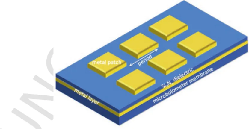
Fig. 19. Schematic of a microbolometer membrane covered by a metamaterial consisting of a metal layer/dielectric (Si3Nx)/periodic metal patch structure.
tion where the plasmonic absorption of the Ag nanocubes occurs, while spin coating on glass leads to composite layers in which absorption is controlled by the amount of embedded cubes. The optical properties of such films depend not only on the natural, size and shape of the metal nanocrystals, but are also function of the spacing and arrangement of the nanocrystals
UNCORRECTED
PROOF
within the embedding film [25]. Near close-packed configuration of nanocrystals and their relative orientation in this packing cre-ate collective behaviors of unique optical signature [26,27]. Controlling aggregation and packing density of nanocrystals inside a hostmatrix can be expected to generate a new class of high performance plasmonic light absorber.
The introduction of nanoparticles in the fluid of a thermal solar module increases the solar radiation absorption when compared to the fluid only. The material and size of the nanoparticles are carefully chosen in order to maximize the absorption and minimize the scattering of the nanoparticles in the spectral domain of interest. Indeed, the maximum solar irradiation intensity is located at 475nm. It has been reported, that the localized surface plasmon resonance absorption peak of core-shell Ag TiO2nanoparticles is
centered around 474nm, making them an ideal candidate to increase the light absorption at the maximum solar irradiation intensity [28]. To increase the absorption on a larger wavelength band, from 250 to 1000nm, nanoparticles made of other materials can be used. It has been shown, that homogeneous Ti and core-shell Ti TiO2, Ni NiO nanoparticles introduced in water at concentrations
of 109- 1010cm−3are suitable to increase the absorption [29].
LSPRs, can also be achieved in semiconductor quantum dots (QDs) with appreciable free carrier concentrations (see Fig. 7) allow-ing active on-chip control of LSPR responses. As shown in Fig. 7, the LSPR frequency can be tuned from near infrared (NIR) to far infrared (FIR) and even THz according the free carrier density and the nanosphere diameter. Thus degenerately doped semiconductor QDs allow realization of LSPRs and quantum-confined excitons within the same nanostructure, opening up the possibility of strong coupling of photonic and electronic modes, with implications for light harvesting, nonlinear optics, and quantum information pro-cessing [30].
Light absorbers are achieved by different means: MIM structures, plasmonic MIM structures or by solely taking advantage of the optical properties of nanoparticles. Each described absorber is based on a different optical phenomenon.
The usage of plasmonic nanoparticles is of particular interest because of the large panel of optical properties they produce. In the recent years, the research on nanoparticle production made huge advances and nowadays a large variety of nanoparticle are produced chemically. This will be described in the following part.
3. Chemical synthesis of nanoparticles of various shapes and sizes
The chemical and physical properties of nanoparticles depend on their material, size, shape and environment. Nanoparticles made from noble metals such as silver and gold are studied for a long time for their extraordinary optical responses attributed to localized plasmon resonances in the visible. As a classical example, the origin of the intriguing colors of the Lycurgus cup, made by ancient Romans, are embedded silver and gold nanoparticles, but the synthesis process was not reported, or got lost over the centuries, mak-ing us believe that it was rather an accidental than wanted process. Faraday conducted the first scientific study of synthesized noble metal nanoparticles in 1857. He reduced gold chloride by phosphorus and analyzed their optical properties. Following this, the ability to tune the optical properties of plasmonic nanoparticles leads the search on syntheses of nanoparticles of different sizes and shapes.
The synthesis methods can be separated into “bottom up” and “top down” approaches. The first approach starts with precursor material and through various reactions individual nanoparticles are produced. The produced nanoparticles present size dispersion, but the quantity is rather high and it is easy to implement. The second approach, “top down”, requires a large amount of energy, which will release nanoparticles from a target, e.g. laser ablation [31], arc discharge [32,33], chemical vapor condensation [33], ball milling [33], hydrogen plasma [33]. The main advantage of the “top down” methods is the high quality and size homogeneity of produced nanoparticles. However, the need for high energy makes the production expensive and mainly limited to applications where only a small quantity of nanoparticles is needed. As a large quantity of nanoparticles is required to efficiently modify the optical properties of thin film layers, this approach is not suitable in this case. On the contrary, chemical wet syntheses allow us to meet this criteria as the wet synthesis process is scalable and economically attractive. This process is therefore described more in details in the following.
From the diversity of existing “bottom up” approaches, e.g. microemulsion [34], thermal decomposition [35], hydrothermal synthesis [36,37], sol-gel [38], sonochemical [39], radiolysis [40], the most commonly used method is chemical reduction of metallic ions by a chemical agent [41–43]. Since roman times, where church glasses were colored intentionally or not by metal
UNCORRECTED
PROOF
L. Escoubas et al. Progress in Quantum Electronics xxx (2019) xxx-xxx
lic dust, tremendous progress has been made in the understanding and developing of wet-chemical syntheses of various materials, shapes and sizes [43]. The nanoparticle growth in chemical syntheses follows a model described in 1950 by LaMer [44] and schema-tized on Fig. 8. Metal salts are dissolved in a solvent and slowly added to the reducing agent solution. On the nanometer scale, ho-mogeneous nucleation occurs in a first step of the synthesis when the minimal concentration for nucleation is reached (Cmin). The
nucleus can then grow or vanish at any time depending on the critical radius in the system. Beyond this critical threshold, all formed nuclei are stable and will grow but below this critical threshold, nuclei are instable and vanish. In the nanoparticle growth step, the stable nuclei grow as long as further metal salts are added and as long as the concentration is above the minimal concentration for heterogeneous growth on seeds (Cmin, seeds). The resulting solution changes then its color, as the nanoparticles grow. If the size
dis-persion is high, a small growth or size reduction might take place over time to make the nanoparticle more uniform. The produced nanoparticles are said to be monodisperse in size when the standard deviation is equal or less than 5%.
The most energetically favorable nanoparticle shape is a sphere. Other shapes are achieved by dividing the nanoparticle growth into two or more synthesis steps. In the specific case of silver nanoparticles, facet-specific capping agent can be used to control the shape evolution of silver nanoparticles in a seed-mediated synthesis. For instance, citrates and PVP were proven to selectively bind to the (111) and (100) facets of silver seeds, respectively, stabilizing these facets more than others and thus favoring the formation of silver nanoparticles with (111) or (100) facets exposed on the surface [45]. Following such strategies, silver nanoparticles could be obtained with various shapes. A non-exhaustive list of produced shapes are: spheres [46], disks [47], plates [42], prisms [48], dumbells [49,50], pyramids [51], cubes [42,43], cages [42], nanowires [42], nanoflowers [52–56], nanostars [57], multipods [58]. It seems that the only limit to nanoparticle synthesis is our imagination. Each of these nanoparticles has then different physical and chemical properties.
For nanospheres, a single reduction step is required. Organic and inorganic reducing agents, such as sodium citrate, ascorbate or sodium borohydride (NaBH4), are used to reduce silver and gold [41–43]. Changing the reaction temperature, stirring speed and
speed at which the solution is added induce a size and size dispersion change [59].
Nanocubes and nanoprisms can be achieved by a two-step seed based synthesis [42,43,46]. The first step produces spherical seeds growing into the desired nanoparticle shape in the second step of the synthesis. Facet-specific capping agents or the solvent itself induce crystallographic defects on the seeds. These defects then induce a face selective growth in the second step of the nanoparticle growth. Indeed, the metal salt added in the second step of the synthesis will preferably be deposited on the other surfaces because the defects are the sites of highest energy [43,46]. Nanocubes are achieved by adding PVP while growing the seeds. In this case, the PVP protects the seeds from aggregating and, as described above, it preferentially binds to the {100} facets leading to a passivation of these facets [42].
After synthesis, the nanoparticles are usually coated with additional surfactant to insure stability of size and shape and prevent aggregation of particles in solution. Common surfactants are sodium citrates [46], sodium borohydride [46] or PVP [42,60,61]. They are added in excess at the end of the synthesis to form a protective shell of a few nanometers around the nanoparticle. Aside the protecting properties, interesting optical properties arise when the polymer shell around the metallic core is modified. Indeed, as plas-monic responses of nanoparticles are environment sensitive, a 5nm thin layer of PVP around synthesized nanocubes can, for instance, shift the absorption peaks wavelength of several tens of nanometers. Other examples occur using inorganic core/shell nanoparticles and were applied for several applications in the biomedical domain [62] (see Fig. 9) such as imaging or sensing [54].
It must be noted that, besides the most studied gold and silver nanoparticles, other plasmonic metallic materials have been devel-oped. For instance, copper nanoparticles can be produced in large quantities by chemical synthesis for applications such as conductive inks [60]. Aluminum also can be synthesized as nanospheres by hydrolysis [64] or as nanowires and nanocubes by plasma arc dis-charge [65]. The major drawback of these materials, however, is their fast oxidation in presence of oxygen, even though the oxidation rate can be reduced [66]. These materials also exhibit high losses at optical frequencies due to electron interband and intraband transitions and their electron densities are not easily tuned. This motivates the search for other plasmonic materials such as doped semiconductors with metal like behavior i.e. oxides, nitrides and chalcogenides [67–70].
The diversity of produced nanoparticles leads to a diversity of chemical and especially optical properties. The optical properties of the described nanoparticles can then either be experimentally characterized once produced or studied by computer modeling. In the following chapter, we firstly describe computer modeling as a convenient tool to foresee the optical properties of the nanoparticles and to validate the measured optical properties, obtained by spectroscopic ellipsometry for instance. In a second part, we describe the spectroscopic ellipsometry measurement technique.
4. Computer modeling and optical characterization of embedded nanoparticles
The optical properties of nanoparticles can be studied by different means. One common and convenient tool is computer modeling. Different simulation and numerical calculation solutions exist for this purpose and will be briefly described in the following: the Mie theory is limited to spherical particles, while the discrete dipole approximation and the finite difference time domain methods can be used for any shape.
In the following, finite difference time domain (FDTD) simulations are described in detail as it is a convenient software to an-alyze the electric field enhancement on the nanoparticles and their optical properties. The geometry of the nanoparticle is freely chosen, as is the environment medium. In particular, the distance between two, or more, neighboring particles can be studied.
UNCORRECTED
PROOF
Different calculation methods, having their advantages and drawbacks, co-exist and must be chosen with care depending on the application. An important feature in calculations and simulations is the material properties, which are either chosen from textbooks, such as from Johnson and Christy [71] or Palik [72], or experimentally measured by spectroscopic ellipsometry.
In simulation using finite element analysis, an important aspect for accurate results is the size and shape of the used mesh. De-creasing the mesh size improves the results, but considerably increases the calculation time. Therefore, the mesh has to be carefully chosen.
The calculation method is chosen depending on the application and the structure of the device. The optical properties of MIM struc-tures can be obtained numerically by transfer matrix method (TMM) [73] and by electromagnetic computer simulations by full-wave solver based on the finite element method. The optical properties of plasmonic nanoparticles are either numerically calculated by Mie Theory, for spherical and ellipsoidal shapes, or simulated by time domain methods, such as FDTD [74], or frequency domain methods, such as FEM [75].
4.2. Mie theory
The optical properties of plasmonic nanoparticles are numerically calculated using the Mie Theory [76]. Mie identified the need for a theory linking the particle size and shape to the optical properties of a colloidal metal solution for particles much smaller than the wavelength. He solved the Maxwell equations for spherical particles of sizes smaller than the wavelength by switching to spherical coordinates, giving an analytical solution for the scattering and absorption of metal nanospheres in any media. The Mie theory can then be applied to calculate the absorption and scattering cross sections. The dipolar absorption σabsand scattering σscatcross section
of a spherical particle depends on the polarizability α of the particle:
where the polarizability depends on the volume V of the particle and the dielectric constants ε of the sphere and εmof
the medium. The derivation of the above equations is described in detail elsewhere [77].
The calculation of the cross sections gives us a first insight on the resonance wavelength of the nanoparticle and whether the nanoparticle will predominately absorb or scatter the incoming light at this wavelength. At the resonance wavelength, plasmonic nanoparticles strongly interact with the incoming light, i.e. the cross section exceeds the geometrical size of the nanoparticle. This simple calculation guides us in the choice of the right nanoparticle material and size with our application in mind. The knowledge of the size of the nanoparticle and the dielectric constant of the nanoparticle and its medium are necessary for the calculation. The cross sections of silver nanospheres are calculated by using the optical indices of bulk silver.
It is worth noting that the Mie theory describes the optical behavior of a single nanosphere in a homogeneous surrounding medium. The interaction and coupling between particles are not taken into account. The Mie theory is therefore useful for colloidal solutions, in which the nanoparticles typically do not interact, and for thin film layers with low nanoparticle density. An analytical formula has been derived for ellipsoidal particles and is typically called Modified Long Wavelength Approximation (MLWA) [78–80]. The formula takes into account the two axes of the particle, which lead to two distinct resonance wavelengths.
The polarizability for an ellipsoid of minor axis a and major axis b is: where ξ0and Χ are size dependent variables.
UNCORRECTED
PROOF
L. Escoubas et al. Progress in Quantum Electronics xxx (2019) xxx-xxx
The Mie theory offers simple equations to calculate the optical properties of nanospheres, but with the emergence of chemical and lithography methods to produce differently shaped nanoparticles such as nanocubes and nanoprisms, the use of the Mie theory is not sufficient anymore. For non-spherical nanoparticles, different methods are used.
4.3. Discrete dipole approximation (DDA)
The absorption and scattering cross sections of arbitrary shaped nanoparticles can be numerically studied by using the discrete dipole approximation (DDA) method. This method was first described in 1964 by DeVoe [81] to calculate the optical properties of molecular aggregates and improved by Purcell and Pennymaker [82] to calculate the optical properties of interstellar dust. The DDA method approximates the studied object with a cubic array of dipoles, each dipole having a defined polarizability. In other words, the object is decomposed into a finite number of points for which the Maxwell equations are solved. The different dipole points interact, i.e. they are electromagnetically coupled. Therefore, the DDA method is sometimes referred to as the coupled dipole approximation (CDA). The accuracy of the calculation strongly depends on the number N of dipoles point chosen, especially for curved surfaces. Increasing N leads to accurate results and increases the computation time consequently. The DDA method is an accurate method to calculate the absorption and scattering cross sections [83]. Dunklin et al. [84] recently showed, that the optical properties of different densities of gold nanoparticles in polymer layers are successfully calculated by DDA. The method also allows a differentiation between dipolar and quadrupolar contribution, which is not straightforward with FDTD simulation. Zhou et al. [85] used DDA calculations to analyze the optical properties of silver nanocubes of edge sizes from 15 to 200nm. The physical origin of each resonance peak is determined, i.e. dipolar and/or quadrupolar resonances, and their size dependence is analyzed. DDA calculations are a convenient tool when used together with experimental measurements to identify the measured absorption and scattering peaks.
4.4. Finite difference time domain (FDTD) simulations
Finite difference time domain (FDTD) simulations [86] allows to simulate the light interaction of particles with any shapes. This is particularly interesting for non-spherical nanoparticles, such as nanocubes, nanoprisms or nanostars produced by facile chemical syn-theses. The optical properties of single nanoparticles, i.e. the absorption, scattering and extinction cross sections, are easily computed and the electric field enhancement on the nanoparticles are visualized. In order to compare the measured optical properties with the simulation, the optical properties of nanoparticles distributed in thin film layer are calculated. In this configuration, the electromag-netic coupling between the nanoparticles in the layer can be studied. FDTD simulations are a convenient tool to verify the optical properties of complex samples, such as multilayers or structured surfaces. The main drawback of FDTD simulations is calculation time. In order to increase the accuracy, especially for curved surfaces, very small mesh cells are chosen, leading to time consuming computation. To counter this, a solution is to work with non-uniform meshed regions with a fine meshing around the nanoparticle, as shown on Fig. 10a. A systematic two step analysis of nanoparticles can be efficiently used: first the nanoparticle alone is studied in different media, such as water and polymer, then the nanoparticles are arranged in a periodic pattern. In the case of non-interacting nanoparticles, in other words electromagnetically isolated particles from each other, the periodic pattern is sufficient. If the distance between the nanoparticles is a few nanometers, the enhanced electric fields will couple and the localized plasmon resonance is af-fected [87]. The study of the nanoparticle alone is mainly performed to obtain the absorption, scattering and extinction cross sections. For this, a total field scattered field source (TFSF) is used, as schematized on Fig. 10b. The electromagnetic radiation is along the blue arrow and its polarization along the purple arrows. The absorption monitor is placed around the particle inside the source region, region 1, and the scattering monitor is placed outside the source region, region 2. Outside the TFSF region, the incident fields are subtracted from the total fields, i.e. only the field scattered by the particle remains.
The cross section is defined by the relation:
where P is the scattered (respectively absorbed) power and I is the source intensity. In the TFSF configuration, the σabsis simply the
complementary to the total cross section measured in the region 1. As only the scattered light reaches region 2, σscatis measured in
UNCORRECTED
PROOF
Long et al. used the electric field enhancement visualization of silver nanospheres to investigate the lasing emission enhancement at the exciting wavelengths. The simulations confirmed the coupling between the plasmonic resonance of the silver nanosphere and the laser emission [91]. Sun et al. [92] analyzed the electric field enhancement of gold-silver core-shell nanorods deposited on dif-ferent thicknesses of a PMMA layer. It was showed that increasing the thickness of the polymer layer has an influence on the electric field enhancement and on the electric field distribution on the nanoparticle. The simulations allowed the authors to determine the optimal PMMA thickness, 56nm, to maximize the electric field enhancement, 27-fold enhancement [92].
For systems where the nanoparticles do not interact, i.e. there is no electromagnetic coupling between the nanoparticles, the study of the nanoparticle alone is sufficient. For systems where the nanoparticles interact with each other, such as in thin film layers of randomly distributed nanoparticles, a second simulation step is necessary to study the effect of the coupling on the optical properties. Different simulation configurations are possible, as the nanoparticles can be distributed in a periodic lattice or pseudo-randomly. The squared lattice distribution is the simplest to implement, as it can be automatically generated, and the fastest in calculation time, as the calculation can be done on a single unit cell. Fig. 12 displays an example of a silver nanoprisms in a squared periodic pattern. The distance between the particles is small enough for the enhanced electric fields to interact.
For pseudo random distributions, different configurations have to be taken into account. Based on the periodic pattern of nanoprisms displayed on Fig. 12, a pseudo random configuration could be obtained by either modifying the orientation of one or more prisms. By turning a prism by 45° or 90°, the incident electromagnetic wave will not exalt the plasmonic resonance in the same manner. An alternative consists on modifying the distance between the nanoparticles to have coupled interactions and uncoupled interactions, i.e. nanoparticles behaving like single nanoparticles.
As an example of specific optical properties obtained from a random distribution of interacting nanoparticles, in a recent theo-retical paper of B. X. Wang [93], a strong-backscattering phase function is studied. It is demonstrated that in particular conditions a disordered medium composed of randomly distributed silicon nanoparticles exhibits a strongly negative scattering asymmetry in the near infrared due to multiple light scattering. As the concentration of scattering particles rises, the backscattering is also enhanced. Predicting and controlling wave propagation in random particulate materials allows people to manipulate the scattering and absorp-tion of radiaabsorp-tion. It paves the way to applicaabsorp-tions such as imaging through turbid media or radiative cooling of coatings by efficient reflection of incident solar power.
To conclude, numerical studies are a convenient way to obtain fast results on the optical properties of nanoparticles and to study their behavior either alone or when electromagnetic coupling occurs.
4.5. Characterization
Following the chosen approach, computations either precede experimental characterization or confirm them. Synthesized nanopar-ticles can be optically characterized as prepared in solution and embedded in a polymer thin film layer. The optical measurements of solutions and of thin films are similar. In the following, only thin films will be considered. In a first step the optical properties, such as transmittance, total reflectance and diffuse reflectance, of the nanoparticles in different media are determined through spec-trophotometric measurements. These quantities are only intensities and strongly dependent on the characteristics of the samples: the thickness of the thin film layers, which changes with the deposition speed, the viscosity of the solution, the ambient temperature or the substrate. Spectroscopic ellipsometry measurements are used to obtain the complex optical indices of the thin film layers, which are independent on the thickness of the layer or the substrate. Spectroscopic ellipsometry is a powerful tool, which requires a general understanding, i.e. the wavelength and broadening of the different absorption or reflection peaks of the samples, as the measured data needs to be fitted with a dispersion model to obtain the optical indices. The general understanding is then either derived from computation or spectrophotometric measurements.
4.6. Spectroscopic ellipsometry
Spectroscopic ellipsometry measurement is an indirect technique to determine either the complex optical indices or the thickness of transparent or semi-transparent thin film layers. These two variables are linked: the knowledge of one is necessary to determine the other.
UNCORRECTED
PROOF
L. Escoubas et al. Progress in Quantum Electronics xxx (2019) xxx-xxx
The knowledge of the complex refractive index allows computing the reflectance and transmittance of any layer thickness on any substrate.
The complex refractive index is the complex addition of the refractive index n and the extinction coefficient k: Fur-thermore, the complex refractive index is closely linked to the complex dielectric function: [94].
A spectroscopic ellipsometry setup is schematized on Fig. 13. The light emitted by the light source is linearly polarized by the polarizer P. Upon reflecting onto the sample, the light becomes elliptically polarized.
To compare the reflected light with the incident light, the light is once again linearly polarized by passing through the analyzer A before reaching the detector. In other words, the measurement consists of the analysis of the polarization change of a reflected light beam by a thin film layer. This is translated into a change of Fresnel reflection coefficients rsand rp, which is measured by the
quantity ρ:
where ψ symbolizes the amplitude change and Δ the phase difference of the reflected light compared to the incident light. Each inter-face yields a different result.
The embedded nanoparticles in the thin film layers are small compared to the wavelength of the light therefore the measurement does not distinguish between the polymer and the nanoparticles, i.e. an effective medium is sensed as schematized in Fig. 14.
The measured properties of the effective medium are an average of the properties of each material, i.e. the inclusions and the polymer matrix. It is supposed to recreate the experimental values and simplify the calculations [95]. Si substrates are typically used to maximize the optical index difference between the two layers. The substrate is assumed to be semi-infinite, i.e. there is no reflected light at the backside of the substrate, and its optical indices are known. Layer 2 on Fig. 14 represents a homogeneous layer of effective indices neffand keff, whose thickness is measured, for example, by a stylus profilometer. The described system has only two interfaces,
but this can also be generalized to a multilayered stack. In the case of a multilayered stack, the thickness of each deposited layer has to be known. Furthermore, it is recommended, that the difference in optical indices of two neighboring layers should be large. If the indices are similar, the phase difference between two layers will not be significant enough to be sensed. The angle at which the measurement is suitably performed is chosen to be near the Brewster angle of the substrate to maximize the intensity of the reflected light [96]. Typically, variable angle spectroscopic ellipsometry (VASE) increases the precision [97].
The complex refractive index of the thin film layer is then determined by fitting these data with an adequate optical model.
4.7. The data fit
The optical model consists of mathematical laws, also called dispersion laws, describing the material of each layer. Once the right optical model is found, iterations verifying the Kramers-Krönig relations are necessary to validate the consistency of the determined indices [98]. Numerous dispersion laws, verifying the Kramers-Krönig relations, exist to account for multiple optical properties of probed materials. Ground knowledge of the optical properties, as the absorbance, is therefore required to choose the right laws and reduce the number of variables of the laws: the spectroscopic ellipsometry measurements are performed combined with spectropho-tometer measurements or numerical calculations. The free variables are then used as fitting parameters to increase the agreement of the calculated data with the experimental ones using the Levenberg-Marquardt method [99] as regression analysis. In the case of visible light absorbing silver nanoparticles dispersed in a non-absorbing polymer layer, the dispersion model is composed of a Cauchy law, accounting for the transparent non-absorbing polymer, and Gauss laws or Lorentz laws, accounting for the different ab-sorption peaks of the plasmonic nanoparticles [100–103]. The suited optical model is chosen by analyzing the model that minimizes the root-mean square error (RMSE) and maximize the coefficient of determination. Furthermore, the obtained indices will be used to compute the reflectance R through a transfer matrix method. The computed R is then compared to the measured R to validate the optical model. The difficulty in the data fit lies in the right choice of dispersion laws and in the number of parameters to vary for each law: a model with one Cauchy law and one Gauss law has six variables. The Cauchy, Gauss and Lorentz laws are described in detail in the following.
4.8. Cauchy law
The Cauchy law typically describes transparent materials:
UNCORRECTED
PROOF
The Gauss law is defined as an oscillator centered at an energy E0, of amplitude Amp and broadening Br. The dielectric function is
then defined as:
where is the full width at half maximum of the oscillator and D is the Dawson's integral [104].
When describing a localized surface plasmon resonance absorption peak with a Gauss oscillator (GO), the energy EOis related to
the measured plasmon resonance energy of the nanoparticles. Amp is related to the intensity and Br to the width of the absorption peak. The use of the Gauss law therefore adds two variables to the analysis.
4.10. Lorentz law
Based on the simple model of a mass and spring system, the Lorentz model describes the classical theory of light-matter interaction and the frequency dependent polarization due to bound charges. The incident electromagnetic field induces vibrations of the electrons behaving as harmonic oscillators.
The Lorentz oscillator (LO) is characterized by an energy E0, an oscillator strength f and a broadening Γ:
The use of the Lorentz law therefore adds two variables to the analysis.
A constant ε∞common to all the complex dielectric functions, e.g. LO and GO, is added to describe the oscillators outside of the
measured spectral domain. This constant is another variable added to the optical model.
4.11. Effective medium theory
When using an effective medium approach, the samples composed of nanoparticles embedded in a host material are considered as a homogeneous material characterized by an effective medium εeffThe Maxwell Garnett formula shown below, allows linking the
effective medium dielectric function to the dielectric functions of each material constituting the effective medium [105,106]. This approach takes into account the first order approximation of the Rayleigh formulae. This simple theory, compared to other such as described in Ref. [107], does not take into account the multiple scattering of the particles in the layer and the polarization of the light. The multiple scattering induces macroscopic optical behavior and is therefore linked to a property of the effective medium. The random orientation of the nanoparticles in the layers should make the optical properties polarization independent. For the results presented in the fourth part of this article, the polymer host matrix is seen as a medium and the silver nanoparticles as inclusions within the medium, therefore:
UNCORRECTED
PROOF
L. Escoubas et al. Progress in Quantum Electronics xxx (2019) xxx-xxx
where δiis the volume fraction of the inclusions and εithe dielectric function of the inclusion, εmis the dielectric function of the
medium and εeffthe dielectric function of the effective medium. For the equation to be valid, the volume fraction should not exceed
one third [81].
Furthermore, the Maxwell-Garnett formula is only valid for spherical inclusions. For spheroids, a factor of depolarization has to be taken into account [99,105,108]. Analytical expressions for other shapes, such as nanoprisms and nanocubes, have not been described yet in the literature.
To conclude, there are a variety of modeling tools to study the optical properties of nanoparticles. FDTD calculations are used for nanoparticles of any shape in any medium, but it must be noted, that the calculation times are long. Then, the experimental character-ization method of spectroscopic ellipsometry is described. The measurement is an indirect technique to determine the effective optical indices of a layer. In order to obtain the optical indices, it is necessary to derive an optical model composed on several dispersion laws. In the following chapter, silver nanospheres and nanocubes randomly embedded in a PVP layer are studied with a suited optical model.
5. Optical properties of plasmonic nanoparticles absorbers
5.1. Optical indices n and k
The knowledge of the optical indices of a thin film layer, determined through spectroscopic ellipsometry, allows a complete un-derstanding of the interaction of light with the layer. In the scope of a highly efficient light absorber, the knowledge of the optical indices of a single layer allows the calculation of multilayers to optimize the absorption. As described above, the determination of the optical indices depends on the right choice of the dispersion model. Different samples and their adapted dispersion models are discussed below.
5.2. The dispersion models
The spectroscopic ellipsometry measurements of noble metal nanoparticles on substrates and embedded within various dielectric matrices are studied by several authors [100–103,109–111]. Concerning the non-absorbing host matrix, the use of a Cauchy law is well established. This is not the case for the optical properties of noble metal nanoparticles as shown on Table 1, which lists the dif-ferent laws used and their physical meaning.
Table 1 gives a broad overview of the different laws used and a guideline for determining the optical model. Depending on the structure of the probed sample, the right model has to be chosen.
In the following, the model composed of a Cauchy law and several Lorentz laws is described in more detail.
5.3. Non-electromagnetically coupled nanospheres and nanocubes in PVP
One interesting example concerns the spectroscopic ellipsometry characterization of a blend of silver nanospheres and silver nanocubes embedded in a PVP thin film. The silver nanospheres in PVP and nanocubes in PVP are firstly characterized independently. Then both shapes, nanospheres and nanocubes, are randomly distributed within the same thin film. In the scope of spectroscopic ellip-sometry measurements, the knowledge of the optical properties of each shape is necessary in order to choose an appropriated optical model. Indeed, the model is composed of a Cauchy law, accounting for the optical properties of the non-absorbing host matrix (PVP in this example), and several Lorentz laws centered at the localized plasmon resonance peaks of the nanospheres and nanocubes. Fig. 15a describes the optical indices of such a layer of nanospheres and nanocubes. The peak centered at 420nm is associated with the dipolar resonance of the nanospheres, while dipolar resonance of the nanocubes is situated at 450nm. The peak centered at 350nm is linked to the cubic shape of the nanocubes. The intensity of each peak is related to the concentration of each type of nanoparticles. For example, by adding more nanocubes to the layer, the intensity of the peaks at 350nm and 450nm is increased. As the nanoparticles in the layer are not electromagnetically interacting, the optical model used to fit the spectroscopic ellipsometry data is a simple ad-dition of the model used for each geometry, nanosphere or nanocube. This is visualized on Fig. 15b, where the normalized extinction coefficient of the layer containing nanospheres and nanocubes is compared to the individual extinction coefficients of nanospheres and nanocubes in separated layers. Electromagnetic coupling between particles in a layer would occur if the distance between the particles is in the order of a few nanometers. This can be achieved by increasing the concentration of nanoparticles in the layer or by forming aggregates [114,115]. The electromagnetic coupling then induces a shifting of the plasmon resonances.
The values of the optical indices n and k (Fig. 15a) are directly linked to the concentration of nanoparticles within the PVP thin film. By increasing the concentration, the absorption at the plasmonic resonance wavelength is increased. In this example, as shown in Fig. 15b, using a blend with two differently shaped nanoparticles, nanospheres and nanocubes, allows a broadening of the absorption from 400 to 600nm.
UNCORRECTED
PROOF
the two first Mie coefficients, one electric and one magnetic, are not negligible. Kerker's conditions correspond to interferences of the dipole scattered fields producing a zero scattering in either the forward or the backward direction. A directional control over the global scattered field can be achieved using the coherent interaction between electric and magnetic resonances. The shape [121] and the size [122] of the nanoparticles and their distance are the main parameters governing Kerker's conditions. In a recent paper by R. Vergaz [123], two nanoparticles satisfying Kerker's conditions in an optimal configuration are presented (see Figs. 16 and 17). Indeed with this dimer of nanoparticles, two interferential effects are possible, one between the scattered field of each nanoparticle and the background-incoming field and one between the scattered fields of each component of the dimer. Thus constructive and destructive interferences appear depending on the distance between the nanoparticles. Then one can control the spatial distribution of light, and more precisely obtain a maximum variation of light intensity in the gap region, by manipulating these interferences. This dimer con-figuration can be used as the base for the design of the all-optical nano-switch.
Fig. 16 describes the system composed of two spherical silicon nanoparticles separated by a distance d, one particle having a radius R1of 82nm and a second one with a radius R2of 97nm. The radius has been chosen such that the first particle (R1=82nm) satisfies
the zero-backward (ZB) scattering condition (see Fig. 156 on the left), while the second one (R2=97nm) fulfills the minimum
for-ward scattering condition (MF) at the incident wavelength 700nm (see Fig. 16a on the right), but there is still an appreciable electric field (red color of the sphere on the illuminated side). Thus the scattered radiation by the nanoparticles can be directed very selec-tively, which allows controlling the overlapping of the fields in a dimer: as a function of the direction of illumination of the dimer, the scattered light can be directed outwards or towards the gap between the nanoparticles. Thus, depending on the illumination side of the dimer, a maximum or a minimum of the scattered field could be observed in gap. For high values of the gap “d”, nanoparticles are considered as isolated and there is no interaction between them but smaller distances allow interferential phenomena to be obtained. In the configuration of Fig. 16a, with light impinging the particle with the largest radius (97nm) from the right, the electromag-netic fields scattered by the particles in the gap are low and as seen in Fig. 17a and b, there is now interference phenomena in the gap. On the other hand, Fig. 17c, which is corresponding to Fig. 16b with light impinging the particle with the smallest radius (82nm) from the left, we observe strong electromagnetic fields scattered by the particles in the gap, but there is a destructive interference phenomena in the gap. By changing the “d” value from 120nm to 445nm, constructive interference can be obtained in the gap as shown in Fig. 17d.
5.5. Collective behavior of aggregates
One example of creating collective response of silver nanoparticle in a controlled way was presented by G. K. Laxminarayana et al. [124]. A novel, modular approach to Ag nanoparticle self-assembly utilizes polymer templating to control meta-atom size and geometry. Colloidal nano-crystals (NCs) are deposited onto the polymer support. They serve as the initial binding platform and are called NCo. Using solvent or thermal annealing of the polymer allows then immobilizing and embedding the NCo into the polymer. Their exposed surfaces are chemically modified with a covalent molecular linker such as a dithiol. Finally, by introducing a second particle (NC1), which reacts with the molecular linker, NC meta-atoms are formed. Repeating this protocol allows producing hierar-chical or dendritic NC motifs (see Fig. 18A–C). Horizontal and vertical nanocube dimers were successfully fabricated with remarkably high yield. As it can be seen in Fig. 18 (G-I), the assembly of the Ag nanocubes into aggregates of controlled number of cubes and organization generates specific optical responses related to their collective properties.
6. Few applications of plasmonic light absorbers
Among the very many articles dealing with localized plasmons and surface plasmons, we highlight here a few applications of par-ticular interest and dealing with spectral filtering and photodetection.
UNCORRECTED
PROOF
L. Escoubas et al. Progress in Quantum Electronics xxx (2019) xxx-xxx
6.1. Spectral filtering
It is possible to create artificial materials able to transmit the visible light and totally absorb the infrared (IR) one. Applications concerns IR blocking plasmonic glass windows. In the articles presented by Y. Qin et al. [125] and L.V. Besteiro et al. [126], the authors use a hexagonal matrix of polystyrene latex spherical nanoparticles (PSL) assembled on a flat silicon substrate. They first perform a reactive ion etching (RIE) process to tune the PSL shape, followed by a magnetron sputtering process of a thin copper or aluminum layer, covering the PSL. By then dissolving the PSL in toluene, they obtain a solution containing copper or aluminum ‘nanocups’. These nanocups, which metal thickness can be controlled by the sputtering time and curvature by the dimensions of the polystyrene nanospheres, exhibit localized plasmons. By adjusting plasmonic absorption peaks, through the nanocup geometric para-meters, authors can thus control the spectral transmission of the windows on which the nanocups are deposited and thus maintain transparency properties in the visible domain while blocking IR.
6.2. Photodetection
T. Maier and H. Brueckl [127] associate a microbolometer, made from a Si3Nx membrane, with a metamaterial absorbing incident
wavelengths in a resonance domain. The metamaterial is directly built above the microbolometer membrane (Fig. 19). It consists of a metal layer/dielectric (Si3Nx)/periodic metal patch structure. The resonance peaks of this structure allow the microbolometer to
become wavelength selective by only optimizing the geometry of the metamaterial elements. This selectivity can be tuned between 2.9μm and 7.7μm by adjusting the dimensions of the metal patchs and their periodicity. The absorption peak can reach up to 88%. The structure is very weakly sensitive to the angle of incidence of radiation because the resonance mode used is of the gap-plasmon type [128] (see part 1). In addition, the use of a metallic layer covering the entire surface changes the conduction heat in the structure by increasing its heat capacity, which leads to an improvement of the response time of the microbolometer.
After excitation, surface plasmons can lose their energy in the form of photon re-emission or non-radiatively in the form of en-ergetic electrons or 'hot electrons’. Recently, hot carriers (hot electrons) have sparked a strong interest because they can be useful for many applications such as photodetection, photovoltaic devices, photocatalysis or surface imaging. Hot carriers are used typically to the photodetection with a structure of Schottky type barrier consisting of a thin metallic layer in contact with a semiconductor material. In the article by W. Li and J. Valentine [129], the authors study the addition of a perfectly absorbing metamaterial at the top of the Schottky barrier (Fig. 20). Thus, they are able to strongly increase the photoresponsivity of the device and obtain a sili-con photodetector sensitive in the infrared domain well below the silisili-con bandgap energy. In addition, the photodetector response is broadband with a photoresponsivity larger than 1.8mA/W for wavelengths ranging from 1200nm to 1500nm and insensitive to the polarization state through the use of square resonators.
7. Conclusion
Beyond simply absorbing light and dissipating this energy into thin composite layers, new applications, such as the all-optical nano-switch previously described, are emerging and are using the coupling of light with nanoparticles. These nanoparticles may ex-hibit various shapes, be alone or apart from each other and therefore without electromagnetic interaction, or even very close in inter-action at a controlled distance and so in resonant electromagnetic regime. They can be aggregated and their morphology controlled by chemical routes, in dimer and multimer forms. They can be in interaction with the substrates and thus constituting Fabry-Perot resonators. These nanoparticles can also be metallic and thus allowing localized plasmons to be excited or be used to generate gap plasmons by the electromagnetic interaction with planar substrates. We also find dielectric nanoparticles presenting electric or mag-netic responses under light excitation and leading to remarkable effects under certain conditions, for example in the Kerker's condi-tions. Thus, by combining the expertise of chemists, able to find original synthesis routes to create, to shape, and to connect these nanoparticles together or with substrates of different natures, and the analysis and models of physicists to understand the interaction of light with these nano-objects, it is already possible to create original components, for example the rectenna or ‘hot electrons’ pho-todetector which directly transforms the light energy into an electrical current. But in the future, it will be possible to create much more complex objects, that we probably can not imagine yet, and whose operating principles will certainly rely on controlled assem-blies of nanoparticles with not only specific optical and magnetic properties but also with quantum properties.
Uncited references