HAL Id: hal-01737300
https://hal.archives-ouvertes.fr/hal-01737300
Submitted on 19 Mar 2018HAL is a multi-disciplinary open access archive for the deposit and dissemination of sci-entific research documents, whether they are pub-lished or not. The documents may come from teaching and research institutions in France or abroad, or from public or private research centers.
L’archive ouverte pluridisciplinaire HAL, est destinée au dépôt et à la diffusion de documents scientifiques de niveau recherche, publiés ou non, émanant des établissements d’enseignement et de recherche français ou étrangers, des laboratoires publics ou privés.
A Built-In Self-Test Structure (BIST) for Resistive
RAMs Characterization: Application to Bipolar
OxRRAM
Hassen Aziza, Marc Bocquet, Mathieu Moreau, Jean-Michel Portal
To cite this version:
Hassen Aziza, Marc Bocquet, Mathieu Moreau, Jean-Michel Portal. A Built-In Self-Test Structure (BIST) for Resistive RAMs Characterization: Application to Bipolar OxRRAM. Solid-State Electron-ics, Elsevier, 2015, 103, pp.73 - 78. �10.1016/j.sse.2014.09.005�. �hal-01737300�
A Built-In Self-Test Structure (BIST) for Resistive
RAMs Characterization: Application to Bipolar
OxRRAM
H. AZIZA, M. BOQUET, M. MOREAU and J-M. PORTAL
IM2NP-Aix-Marseille University, 38, Rue Frédéric Joliot-Curie, 13451, Marseille, France.
* Corresponding author: H. AZIZA
Address: IM2NP, Technopôle de Château-Gombert
38, Rue Frédéric Joliot-Curie, 13451 Marseille Cedex 20, France
Office: (33)-491-054-784 Fax: (33)-491-054-782 Email: [email protected]
Abstract — Resistive Random Access Memory (RRAM) is a form of nonvolatile storage
that operates by changing the resistance of a specially formulated solid dielectric material [1]. Among RRAMs, Oxide-based Resistive RAMs (so-called OxRRAMs) are promising candidates due their compatibility with CMOS processes and high ON/OFF resistance ratio. Common problems with OxRRAM are related to high variability in operating conditions and low yield. OxRRAM variability mainly impact ON/OFF resistance ratio. This ratio is a key parameter to determine the overall performance of an OxRRAM memory. In this context, the presented built-in structure allows collecting statistical data related to the OxRRAM memory array (ON/OFF resistance distributions) for reliability assessment of the technology.
Keywords — Resistive RAM, OxRRAM, Reliability, Test, Built-In Self-Test Structure
1 I
NTRODUCTIONIn RRAM, the data is stored as two or multiple resistance states of the resistive switching device. Resistive switching in transition metal oxides was discovered in thin NiO films decades ago [1]. Since then, a large number of materials showing a resistive switching have been reported in the literature [2-4]. Among them, metal oxides as HfO2, NiO, TiO2 or Cu2O
are promising candidates due their compatibility with CMOS processes. In its simplest form, resistive memory element relies on a Metal/Insulator/Metal (MIM) stack that can be easily integrated into the Back-End Of Line (BEOL), paving the way for 3D technology. In the same time, new architectures are investigated to provide higher performances [5] [6].
OxRRAM presents a lot of interesting features like high integration density, high-speed operations (write/erase/read) and satisfactory reliability performances in terms of retention and cycling. Hence, OxRRAM memory has been a leading candidate among emerging technologies. However, this technology is still in its “infancy” since the physics of resistance switching is not yet fully understood. So far, it is broadly accepted that the electro migration of oxygen vacancies plays a critical role in the resistance switching. Although OxRRAM-based devices have shown encouraging properties, challenges remain, among which the device variability (or reproducibility) is the main [7]. The variance from switching cycle to cycle and from device to device can be very large. For example, it has been seen experimentally that variability can vary in the range 2x-10x for the ON resistance and 5x-100x for the OFF resistance in Cu2-O-based devices [8].
In OxRRAM memories, MIM structures are used as a single-bit memory cell, while the semiconductor transistor subsystem enables performing all the peripheral operations (input/output, coding/decoding, line driving, and sense amplification) [9]. During the early phase of development it is often difficult to obtain sufficiently reliable data on OxRRAM
memories. Indeed, the process itself is not stabilized and fully functional devices are not yet available. Moreover, a suitable OxRRAM chip currently does not exist and the technology, although rapidly evolving, is currently not sufficiently mature.
In this context, the presented study proposes a Built-In Self-Test Structure (BIST) to evaluate OxRRAM variability at a circuit level. The presented built-in structure allows collecting statistical data related to the OxRRAM memory array. Basically, ON/OFF resistance distributions are extracted at a circuit level, during a READ operation, in a specific test mode without impacting the circuit normal working operation.
Section II introduces OxRRAM technology. Section III presents in detail the BIST circuit. In section IV, simulation results are provided and section V concludes the paper.
2 O
XRRAM
T
ECHNOLOGYIn memory devices relying on a resistance change, complex physical mechanisms are responsible for reversible switching of the electrical conductivity between high and low resistance states. The resistivity change is generally attributed to the formation/dissolution of conductive paths between metallic electrodes. Various mechanisms may explain the resistance change (oxygen vacancy migration [4], oxidation-reduction processes, thermal diffusion…).
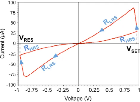
In working conditions, after an initial electroforming process, the OxRRAM element may be reversibly switched between reset (high resistance) and set states (low resistance). Electroforming stage corresponds to a voltage-induced resistance switching from an initial very high resistance state (virgin state) to a conductive state. In the literature, unipolar, bipolar and non-polar electrical behaviors are reported. In the case of bipolar switching, addressed in this paper, bipolar voltage sweeps are required to switch
the memory element (Fig. 1). Resistive switching in an OxRRAM element corresponds to an abrupt change between a High Resistance State (HRS or OFF state) and a Low Resistance State (LRS or ON state). This resistance change is achieved by applying specific voltage to the structure (i.e. VSET and VRES). Based on the memory cell
hysteresis presented in Fig. 1, in a first approximation, four OxRRAM critical reliability parameters can be considered: VSET, VRES, RHRS and RLRS.
3 S
IMULATIONC
IRCUIT3.1 Circuit architecture
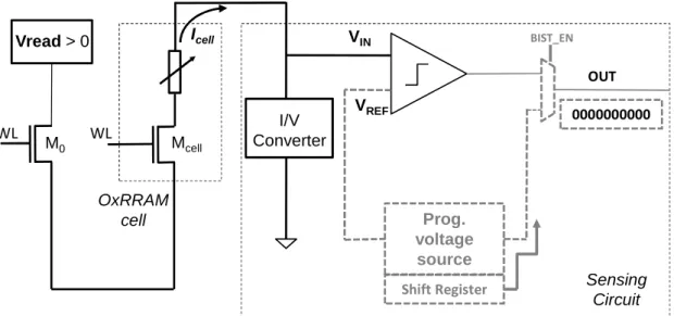
Fig. 2 presents the elementary array used for simulation which is constituted of a 3×3 1T/1R cell matrix, a row decoder, a column decoder and a sense amplifier for the READ operation. The resistor is actually an OxRRAM model presented in the next section. The 1T/1R memory cell (one MOS transistor in series with one resistor) is seen as an effective alternative to replace embedded DRAM-based memory modules by substituting the capacitor by an OxRRAM resistor.
Fig. 3 presents the single-ended sense amplifier (solid line). The circuit working principle is quite simple. During a READ operation, the OxRRAM cell is biased through the row decoder (with Vread > 0 and WL high). The current cell value (Icell) is generated
according to the memory state (RON ~ 7kΩ after a SET operation and ROFF ~ 25 kΩ after a RESET operation). Notice that Mcell sizing is critical in terms of current
consumption during the programming phase. Indeed, the clamping effect of the select transistor reduces drastically the cell current.
The comparator input VIN is directly proportional to the cell current Icell and therefore to
RESET for ROFF). So that the sense amplifier operates properly, on the one hand the
difference between VIN SET and VIN RESET must be the highest and on the other hand VREF
has to be set exactly between VIN SET and VIN RESET values.In these conditions, the logical
value of the cell is correctly sensed and available at the sense amplifier output (OUT).
3.2 BIST implementation
At a circuit level, VIN is the parameter to consider in terms of memory functionality. To
extract VIN value, the classical single-ended sense amplifier architecture is modified. A
programmable voltage source and a multiplexer are incorporated in the sensing circuit design (Fig. 3, dotted lines) and the READ operation is modified as follow:
• VREF is first set to ground,
• VREF increases step by step from 0 to Vdd (VREF increase is controlled by a shift
register),
• VIN value is detected when VREF reaches VIN (i.e. VREF > VIN is detected when the
sense amplifier output switches),
• VIN is available at the circuit output in a numerical value if BIST_EN signal is set high.
The programmable voltage source is presented in Fig. 4a. Each step of VREF is
performed by switching on successively programmable switches. The transmission gates of the voltage source are controlled by the shift register presented in Fig. 4b, which shifts a “1” and has all its other bits set to “0”. The shifting process stops when the sense amplifier output switches. At this point, the content of the register is shifted out via the sense amplifier output.
BIST structure is common to the entire memory array, which reduces the area overhead. The test time overhead is related to the number of programming voltage source steps. In the example presented Fig. 4b, the shift register is designed to perform 20 cycles of consecutive readings, which represents a good tradeoff between VIN SET and VIN RESET
distribution accuracy and test time overhead.
3.3 OxRRAM cell Model
The elementary array used for simulation embeds an OxRRAM model. The proposed OxRRAM modeling approach relies on electric field-induced creation/destruction of oxygen vacancies within the switching layer. The model enables continuously accounting for both SET and RESET operations into a single master equation in which the resistance is controlled by the radius of the conduction pathways (rCF) [10].
(
)
k T V q Ea CF T k V q Ea CF CF CF b cell ox dOx b cell red dOxe
r
e
r
r
dt
dr
⋅ ⋅ ⋅ + − ⋅ ⋅ ⋅ − −⋅
⋅
−
⋅
⋅
−
=
α β α βRe10
Re10
max (1)where βRedOx is the nominal oxide reduction rate, Ea is the activation energy, αred and αox are the transfer coefficients (ranging between 0 and 1), kb is the Boltzmann constant, T is the temperature and Vcell the voltage across the cell.
Moreover, the model makes assumptions of a uniform radius of the conduction pathways, a uniform electric field in the cell and temperature triggered acceleration of the oxide reduction reactions (“redox”). Finally, the total current in the OxRRAM includes two components, i.e. one is related to the conductive species (IFC) and the other to the conduction through the oxide (IOX).
(
)
(
CF CF OX CF OX)
x Cell CFr
r
L
V
I
=
⋅
π
⋅
2⋅
σ
−
σ
+
π
⋅
2 max⋅
σ
(2) HRS x Cell Cell HRS OXL
V
S
A
I
β
⋅
=
(3)where Lx is the oxide thickness, SCell is the total area of the device, σOx the oxidation
rate and σCF the reduction rate. To take into account IOX trap assisted current
(Poole-Frenkel, Schottky emission, Space Charge Limited Current (SCLC)), a power law between the cell current and the applied bias is considered with two parameters AHRS
and βHRS. Finally, the total current flowing through the cell is:
OX CF
Cell
I
I
I
=
+
(4)ICF is the main contributor to LRS current (ILRS) and IOX is the main contributor to HRS
current (IHRS).
The memory cell compact model is calibrated on silicon. The model was confronted to quasi-static and dynamic experimental data before its implementation in electrical circuit simulators. As presented in Fig. 5a, after calibration, the model satisfactorily matches quasi-static and dynamic experimental data measured on actual HfO2-based memory
elements (TiN/Ti/HfOx/TiN stack reported in [11]). To program a bipolar OxRRAM cell, a
voltage ramp is needed. In Fig. 5b, the evolution of SET voltages as a function of the ramp speed is presented. The model implementation focused on this dependence, crucial for the model to be confidently implemented in circuit simulators.
Due to the stochastic nature of the switching process in OxRRAMs, leading to large variability, the OxRRAM model features a variability dependency. The cell variability
modeling is based on OxRRAM card model parameter variations. The variation is chosen to fit circuit experimental data as presented in Fig. 6. A good agreement with experimental data is obtained for [βRedOx±5% and βHRS ±1.5%] (i.e. βRedOx and βHRS are
included in the range ±5% and ±1.5% respectively, of a distribution following a Gaussian law). At an electrical level, these variations directly impact ON/OFF resistances.
4 S
IMULATION RESULTSThe elementary matrix presented in Fig. 2, embedding the BIST structure presented en Fig. 3, is considered for simulations. Since cell variability is generated based on a targeted technology and memory array architecture, only the realistically possible variations are reported [12] [13].
To validate the BIST structure, a straight correlation between memory cell variability and the sense amplifier output is first established. Then, an application example dealing with the sense amplifier characterization versus variability is presented.
4.1 BIST structure validation
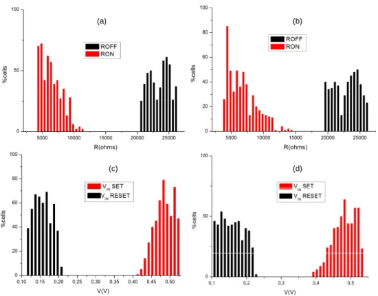
In this study, a large number of Monte Carlo simulations are performed to provide the statistic needed to characterize variability and its impact on the circuit. Cell variation is introduced and simulated sequentially using an electrical simulator. The goal is to track an important shift of the OxRRAM reliability parameters (RON and ROFF). The memory array programming is done in 2 cycles. First, all memory cells are SET (logical “1”), then the memory array is RESET (logical “0”). Logical failures can be detected at the output of the sense amplifier during a read operation after SET/RESET cycles. Variability is introduced through the two model card parameters βRedOx and βHRS.
In Fig. 7a, RON and ROFF distributions are plotted for cell variability included in the range [βRedOx ±5% and βHRS ±1.5%]. In Fig. 7b, cell variability is increased and included
in the range [βRedOx ±10% and βHRS ±3%]. An important spreading of RON and ROFF
parameters is observed in Fig. 7b. Indeed, the initial spreading of RON and ROFF distributions increases according to the variability increase.
In Fig.7c and Fig.7d, VIN SET and VIN RESET distributions obtained using the BIST structure
are plotted. These distributions are similar to RON and ROFF distributions obtained in Fig.7a and Fig.7b respectively. Indeed, VIN represents the image of the current flowing
through the OxRRAM cell. This trend is confirmed by the correlation curve presented in Fig. 8. Therefore, the modified sense amplifier structure can be used as a powerful tool to track any resistance variations but also to characterize the memory array variability.
4.2 Sense amplifier characterization
Fig. 9 presents an analysis of VIN SET and VIN RESET distributions versus the reading
voltage VREAD. For each VREAD value, 100 Monte Carlo simulations are performed after a
SET and a RESET operation to extract the sense amplifier VIN distributions. Fig. 9
proposes also an evaluation of the cell consumption distributions during a read operation (reported on the left side of the graph, in Femto Joule, which corresponds to the product of the voltage by the current during the READ time). This information is important and underlines the need of a tradeoff between robustness and consumption. For instance, for mobile applications containing OxRRAMs, the trend would be to reduce the cell consumption without compromising reliability.
For instance, to have the highest difference between VIN SET and VIN RESET while
350mV (dotted lines in Fig. 9). As OxRRAM technology suffers from cell to cell variability, the use of reference cells to obtain a reference voltage to read memory elements is prohibited. Thus, a BIST structure capable to determine on the fly, at a circuit level, the suitable reading voltage reference is a powerful tool for designers to provide robust bipolar OxRRAM memory circuits.
5 C
ONCLUSIONA Built In Self-Test (BIST) structure is presented for Resistive RAM memories characterization and variability evaluation. The area overhead introduced by structure is relatively low as the structure is integrated in the sense amplifiers. The normal operation mode of the memory circuit is preserved. Besides, extracted values are given in a digital data format, so the extraction process does not required any analog pin on the tester, making it fully digital tester compliant or easily observable via the random logic. As variability in OxRRAMs presents a major challenge for fabrication process and design engineers, the BIST structure can be used to quickly evaluate cell variability impact on the ON/OFF resistance ratio of a whole memory array. From a design point of view, BIST data can provide interesting guidelines at a circuit level to design robust bipolar OxRRAM memories.
R
EFERENCES[1] F. Gibbons & al, “Switching properties of thin Nio films”, Solid-State Electronics, vol. 7, issue 11, pp. 785-790. (1964).
[2] S. Seo & al., “Reproducible resistance switching in polycrystalline NiO films,” Appl. Phys. Lett., Vol. 85, No. 23, p. 5655 (2004).
[3] Wan Gee Kim & al., “Dependence of the switching characteristics of resistance random access memory on the type of transition metal oxide,” European Solid-State Device Research Conferenc, pp. 400-403 (2010).
[4] Hyo-Shin Ahnl & al., “Pairing of cation vacancies and gap-state creation in TiO2 and HfO2,” Appl. Phys. Lett., Vol. 90, Iss. 25, pp. 252908-252908-3 (2007).
[5] W.S. Zaho & al, “Crossbar architecture based on 2R complementary resistive switching memory cell”, Proceedings of IEEE International Symposium on Nanoscale Architectures (NANOARCH), pp. 85-92 (2012).
[6] W.S. Zaho & al, “Synchronous Non-Volatile Logic Gate Design Based on Resistive Switching Memories”, Circuits and Systems I: IEEE Transactions on Volume: PP, p 12 (2013).
[7] H. Aziza & al, “Evaluation of OxRAM cell variability impact on memory performances through electrical simulations”, Non-Volatile Memory Technology Symposium (2011).
[8] An Chen & al., “Variability of resistive switching memories and its impact on crossbar array performance”, Proceedings of the IEEE International Reliability Physics Symposium (IRPS), pp. MY.7.1 - MY.7.4 (2011).
[9] H. Aziza & al, “Bipolar OxRRAM memory array reliability evaluation based on fault injection”, International Design and Test Workshop, pp. 78-81 (2011).
[10] M. Bocquet, D. Deleruyelle, H. Aziza, C. Muller, J-M. Portal, “Compact modeling solutions for OxRAM memories”, IEEE Proc. Of Faible Tension Faible Consommation (FTFC), pp. 1-4 (2013).
[11] T. Diokh, “Investigation of the Impact of the Oxide Thickness and RESET conditions on Disturb in HfO2-RRAM integrated in a 65nm CMOS Technology”, in International Reliability Physics Symposium , pp. 3-6 (2013).
[12] H. Aziza, JM. Portal, D. Nee, C. Reliaud, F. Argoud, “Peripheral Circuitry Impact on EEPROM Threshold Voltage”, IEEE Proc. Of Non-Volatile Memory Technology Symposium (NVMTS), pp. 20-24 (2007).
[13] H. Aziza & al., “Speeding up simulation time in EEPROM memory designs,” Int. proc. of nternational Conference on Design & Test of Integrated Systems in Nanoscale Technology (DTIS), p. 285-288 (2006).
Figure 1. Typical I-V characteristic of a bipolar OxRRAM cell
I/V Converter OxRRAM cell Prog. voltage source WL VIN Vread > 0 Sensing Circuit WL OUT Icell Mcell M0 VREF 0000000000 Shift Register BIST_EN
Figure 3. OxRRAM sensing circuit
1000 0000 0000 0000 0000 0100 0000 0000 0000 0000 0010 0000 0000 0000 0000 0001 0000 0000 0000 0000 0000 1000 0000 0000 0000 0000 0100 0000 0000 0000 0000 0010 0000 0000 0000 0000 0001 0000 0000 0000 0000 0000 1000 0000 0000 0000 0000 0100 0000 0000 VREF 2.VREF 3.VREF 4.VREF 5.VREF 6.VREF 7.VREF 8.VREF 9.VREF 10.VREF C0 C20
Shift Register Outputs
Vin P r o g r a m m a b le s w it c h V o lt a g e r e f e r e n c e s C o n t r o l G a t e in p u t VR E F 2 . VR E F 3 . VR E F Vin P r o g r a m m a b le s w it c h V o lt a g e r e f e r e n c e s C o n t r o l G a t e in p u t VR E F 2 . VR E F 3 . VR E F (a) (b)
-1.5 -1.0 -0.5 0.0 0.5 1.0 10-9 10-8 10-7 10-6 10-5 10-4 10-3 0.0 0.5 1.0 10-9 10-7 10-5 10-3 10-1 101 103 105 Simu. Data [9] Set Reset (a)
I
C e ll(
A
)
V
Cell(V)
(b)T
S e tV
App Simu. Data [9](s
)
(V)
Figure 5. I-V characteristic measured on HfO2-based devices (a) [11] and corresponding
simulation using a bipolar OxRRAM physical model. Set voltage as a function of the programming ramp (b) -1.5 -1.0 -0.5 0.0 0.5 1.0 10-9 10-8 10-7 10-6 10-5 10-4 10-3 Lines: Simu. Symbols: Data [9]
I
C e ll(
A
)
V
Cell(V)
[11]Figure 6. RON and ROFF distributions versus cell variability. Model calibrated on experimental data for specific card model parameter variation [βRedOx±5% and βHRS ±1,5%]
(a)
(c)
(b)
(d)
Figure 7. RON and ROFF distributions versus cell variability after 500 Monte Carlo runs. Cell variability included in the range [βRedOx±5% and βHRS ±1.5%] (a) and in the range
[βRedOx±10% and βHRS ±3%] (b). Corresponding SET/RESET VIN voltage distributions (d), (e).
C o n s u m p ti o n ( fJ ) 90 50 40 30 20 10 0 80 70 60 VREF
Figure 8. VIN SET and VIN RESET distributions versus cell variability [βRedOx±5% and βHRS ±1.5%]
![Figure 6. RON and ROFF distributions versus cell variability. Model calibrated on experimental data for specific card model parameter variation [ β RedOx ±5% and β HRS ±1,5%]](https://thumb-eu.123doks.com/thumbv2/123doknet/14663050.740129/16.892.224.637.656.962/figure-distributions-variability-calibrated-experimental-specific-parameter-variation.webp)
![Figure 8. V IN SET and V IN RESET distributions versus cell variability [β RedOx ±5% and β HRS ±1.5%]](https://thumb-eu.123doks.com/thumbv2/123doknet/14663050.740129/18.892.151.748.142.580/figure-set-reset-distributions-versus-cell-variability-redox.webp)
