Amplitude and Phase Modulation Techniques for an
Asymmetric Multi-Level Outphasing Transmitter
by
Gilad Yahalom
Submitted to the Department of Electrical Engineering and Computer
Science
in partial fulfillment of the requirements for the degree of
Master of Science in Electrical Engineering
at the
MASSACHUSETTS INSTITUTE OF TECHNOLOGY
ARCHIVES
ITUTE
2131
September 2012
@
Massachusetts Institute of Technology 2012. All rights reserved.
A uthor
. .
.
...
...
Department of Electrical Engineering and Computer Science
Aug 29, 2012
Certifiedby...,..
...
Joel L. Dawson
Associate Professor
Thesis Supervisor
Accepted by ...
Leshb(OA.(kolodziej ski
Chairman, Department Committee on Graduate Theses
Amplitude and Phase Modulation Techniques for an Asymmetric
Multi-Level Outphasing Transmitter
by
Gilad Yahalom
Submitted to the Department of Electrical Engineering and Computer Science
on Aug 29, 2012, in partial fulfillment of the
requirements for the degree of Master of Science in Electrical Engineering
Abstract
New techniques for improving outphasing transmitters show potential of breaking the tra-ditional linearity-efficiency trade-off by using highly efficient non-linear switching Power Amplifiers (PAs). This work focuses on two of the main building blocks of modem out-phasing systems, the power supply switching network and the phase modulator. Both are ubiquitous building blocks in modern RF transceivers, and both are especially critical in Asymmetric Multilevel Outphasing (AMO) systems.
A design of the power supply network and control scheme is proposed for an
imple-mentation in mm-wave operating frequencies as part of a complete transmitter in 45nm
SOI CMOS utilizing four discrete power supplies and achieving data rates of up to 4GS/s.
The design includes analysis and simulation of the control signal data path requirements for optimal system operation as well as switch optimization and effects of the driving strength on overall system performance.
A new design concept is proposed for a phase modulator utilizing the phase shifthing
capabilities of a resonant tank and the ability to seperately control the circuit properties via its components. A prototype in 65nm CMOS achieves 12 bits of resolution, with an Effective Number Of Bits (ENOB) of 10.2 bits and very fast settling time of less than 5
carrier cycles. The chip is also tested as a stand alone transmitter showing an EVM of less than 5% for 8-PSK modulation at maximum data rate, meeting the requirements for operation at the Medical Implant Communication Services (MICS) band.
Thesis Supervisor: Joel L. Dawson Title: Associate Professor
Acknowledgments
I would like to thank Professor Joel Dawson for all his support during my work on this Thesis and helping me along my journey so far through MIT. His encouragmenet and good advice were invaluable to the success of this work. His wealth of knowledge and openess to new ideas and directions allowed me to reach out and explore wider areas and branch out to new directions and helped me overcome many of the hurdles along the way, all the while creating a friendly and extremely pleasent work environment in his group.
I would also like to thank Professor Vladimir Stojanovic, Professor David Ricketts and
Dr. Yehuda Avniel for many helpful discussions and reviews of the work, each highlighting different aspects and helping realize better solutions with a broader system view.
My Colleague and teammates Taylor Barton, SungWon Chung, Zhen Li and Sushmit
Goswami for countless discussion and consoltations and having the patience to hear me detail my problems and numerous bugs. I would also like to thank Philip Godoy and John Spaulding whose research is the basis my work is laid upon. Yan Li and Zhipeng Li for assisting and leading the digital side of the project and Wei Tai and Chongzhe Li for their PA and combiner work, great help and many useful tips during layout and final tapeout.
I'd also like to thank Professor Anantha Chandrakasan who helped secure foundry
ser-vices from TSMC which enabled the realization of the proof-of-concept phase modulator design presented in this work.
Finally, Nothing in my career could ever get done without the endless support and patience from my lovely wife Emanuel - Thanks for being there for me and believing in me.
Contents
List of Figures 9 List of Tables 13 List of Acronyms 15 1 Introduction 17 1.1 Motivation. . . . . 17 1.2 Linear Transmitter . . . . 18 1.3 Polar Transmitter . . . . 19 1.4 Outphasing Transmitter . . . . 211.5 Asymmetric Multilevel Outphasing (AMO) Transmitter . . . 22
1.6 Research Contributions . . . 24
2 Amplitude Modulation 27 2.1 Introduction . . . 27
2.2 Power Supply Switch Network . . . 28
2.2.1 Switch Design . . . 29
2.2.2 Time Alignment . . . 36
2.2.2.1 Nulling Test . . . 38
2.2.3 Decoding and Overlap Control . . . 40
2.2.4 Level Shifting . . . 42
2.2.5 Slew Rate Control . . . 45
3 Phase Modulation
3.1 Introduction . . . .
3.1.1 Digital to Analog Converter (DAC)
3.1.2 Current Steering DAC . . . . 3.2 Low-Q Resonant Tank Phase Modulator .
3.2.1 Design Process . . . .
3.2.2 Switched Capacitor Bank . . . . .
3.2.3 Active Resistor . . . . 3.2.3.1 Constant g,, Reference 3.2.4 RC Polyphase Filter . . . . 3.3 Measurement Results . . . . 3.3.1 Capacitor Trim . . . . 3.3.2 Resistor Trim . . . . 3.3.3 Static Sweep . . . . 3.3.4 Settling Time . . . .
3.3.5 Error Vector Magnitude (EVM) .
3.3.6 Power Spectrum . . . . 3.4 Summary . . . . A Data A.1 A.2 A.3 A.4 51 . . . . 5 1 Phase Creation . . . . 52 . . . 5 5 . . . . 5 5 . . . . 6 0 . . . . 62 . . . . 6 3 . . . . 6 5 . . . . 6 7 . . . . 6 8 . . . . 7 0 . . . . 7 1 . . . . 7 2 . . . . 7 5 . . . . 7 7 . . . . 7 9 . . . 8 1 Demodulation Test Setup . . . . Demodulation Procedure . . . . Error Vector Magnitude (EVM) Calculation Power Spectral Density (PSD) Calculation
83 83 84 89 92 93 Bibliography
List of Figures
1-1 64-QAM constellation diagram . . . .
1-2 Linear transmitter . . . .
1-3 Constant envelope transmitter . . . .
1-4 Polar transmitter . . . .
1-5 LINC transmitter . . . .
1-6 Multilevel LINC operating principle . . . .
1-7 AMO transmitter . . . .
1-8 Ideal efficiency comparison between LINC, ML-tures .... ...
2-.1 Poiwrer s11u lsi0tchin n at;wrkl aia ram
2-2 Supply level usage histogram
2-3 2-4 2-5 2-6 2-7 2-8 2-9 2-10 2-11
Switch conduction losses . .
Gate capacitance . . . .
Switch switching losses . . .
Switch total power loss . . .
Switch weighted power loss Delay cell element... PVT corner simulation of dela Amplitude path misalignment 2-to-4 Decoder . . . . 2-12 Overlap control scheme
*LINC and AMO architec-18 19 20 20 21 22 23 24 9 , "I'll"7 . . . . . . . . . . . .... . . . . 30 . . . . 32 . . . . 33 . . . . 34 . . . . 34 . . . . 35 . . . . 37 y cell . . . . 38 of 100ps . . . . 39 . . . . 40 . . . . 41
Level shifter schematic . . . . Linear slope as convolution of two square waves . Added attenuation due to varying slopes . . . . . Output spectrum for various rise times . . . . (a) Output slope rise time and (b) zoom-in . . . .
Static delay caused by slew rate control . . . . .
3-1 Phase modulation via two DACs . . . .
3-2 DAC Phase Modulator (PM) control option examples . .
3-3 DAC PM amplitude variation . . . .
3-4 DAC PM phase variation . . . .
3-5 Parallel RLC tank . . . .
3-6 Phase modulator resonant tank concept . . . . 3-7 Phase coverage at different quality factors . . . . 3-8 Resonant tank phase coverage . . . .
3-9 Chip micrograph . . . .
3-10 Switched capacitor element cell . . . . 3-11 OTA as resistor element . . . .
3-12 OTA schematic . . . .
3-13 Current reference schematic . . . .
3-14 Theoretical effective resistance value . . . .
3-15 RC polyphase filter schematic . . . .
3-16 One stage RC Polyphase filter response . . . . 3-17 Two stage RC Polyphase filter response . . . . 3-18 Phase quadrant imbalance vs. fixed capacitor size trim 3-19 Quadrant phase coverage for various resistor trim values 3-20 Quadrant size as a function of resistor size trim . . . . . 3-21 Static phase sweep . . . . 3-22 DNL measurement of raw phase sweep . . . . 3-23 Static phase sweep with pre-distortion . . . .
. . . . 52 . . . . 53 . . . . 54 . . . . 54 . . . . 56 . . . . 57 . . . . 58 . . . 59 . . . . 61 . . . 62 . . . 64 . . . 64 . . . 65 . . . 67 . . . 68 . . . 69 . . . 69 . . . 70 . . . 71 . . . 72 . . . 73 . . . 74 . . . 74 2-14 2-15 2-16 2-17 2-18 2-19 44 46 47 47 49 50
3-24 DNL after pre-distortion and resolution reduction . . . . 75
3-25 (a) Phase step settling time and (b) zoom-in . . . 76
3-26 EVM measurements for QPSK modulation at 40 MS/s . . . . 78
3-27 EVM measurements for 8-PSK modulation at 40 MS/s . . . . 78
3-28 8-PSK modulation output PSD overlaid with MICS mask . . . 80
3-29 (a) GMSK modulation output PSD overlaid with GSM mask and (b) zoom-in 81 A-1 Measurement setup . . . . 84
A-2 Reference and PM output data from scope capture. Data rate is 1OMS/s, carrier frequency 416.67MHz, sampling rate 40GS/s . . . . 85
A-3 Modulated PM output (only real part displayed) . . . 85
A-4 Low-pass filter frequency response . . . . 86
A-5 Demodulated normalized data, showing real (In-phase) and imaginary (Quadra-ture) components . . . . 88
A-6 Demodulated normalized data, showing phase. Sample points are indicated by circle markers . . . . 88
A-7 EVM definition plot . . . . 89
List of Tables
List of Acronyms
AM Amplitude Modulation
AMO Asymmetric Multilevel Outphasing
CMOS Complimentary Metal-Oxide-Semiconductor
CPM Continuous Phase Modulation
DAC Digital to Analog Converter
DNL Differential Non-Linearity
EER Envelope Elimination and Restoration
ENOB Effective Number Of Bits
ETSI European Telecommunications Standards Institute
EVM Error Vector Magnitude
FCC Federal Communications Commission
FET Field Effect Transistor
FM Frequency Modulation
FPGA Field Programmable Gate Array
GMSK Gaussian Minimum Shift Keying
IF Intermediate Frequency
ISM Industrial, Scientific and Medical
LSB Least Significant Bit
LINC Linear Amplification with Nonlinear Components
MICS Medical Implant Communication Services
MIM Metal-Insulator-Metal
MSK Minimum Shift Keying
OSR Oversampling Ratio
OTA Operational Transconductance Amplifier
PA Power Amplifier
PCB Printed Circuit Board
PM Phase Modulator
PSD Power Spectral Density
PSK Phase Shift Keying
PTAT Proportional to Absolute Temperature
PVT Process, Voltage and Temperature
QAM Quadrature Amplitude Modulation
QPSK Quadrature Phase Shift Keying
RF Radio Frequency
RMS Root Mean Square
SNR Signal to Noise Ratio
Chapter 1
Introduction
1.1
Motivation
There is an ever increasing demand for higher data rates in wireless communication to support new applications and content. In conjunction with this demand for speed, there is a persistent requirement for efficiency and low power consumption to enable portability and reduce energy waste.
There is a traditional trade-off between efficiency and linearity in Power Amplifiers (PAs). High linearity translates directly to higher data rates, as more information can be embodied in the transmitted signal, and this is employed in many modem communication modulation schemes such as 64-QAM, where each symbol transmitted may correspond to one of 64 (6 bits) data points on the Cartesian plane. Figure -1-1 illustrates this concept. We can see that each symbol can be characterized by a vector with its head at the symbol point, with a varying amplitude and phase component, or alternatively a real (In-phase) and imaginary (Quadrature) part.
On the other hand, high efficiency PA types, such as switching PAs, usually have very high efficiency at their maximum power output. Although, on the face of it, switching PAs are incapable of modulating their output power. Until recently, this has rendered them useful only in low data rate applications.
These trade-offs however, are not fundamental, but are more strongly related to the
Figre -1:4-A constell0"Actin diagraDom 1001 14401t 1011 101W0 00100 =o 010 00010 001 eaiyad fii0 e0 1 ai0101 100111 101".11P1011 w 41 Willi1 005111 011000101 4** '*Il * WX 10o0100tv11h yM 1011 0stellato p0 000 l F r 12 .11"100 110)0 1161 111100 0)1)0 01110 010110 010)00
Figure 1-1: 64-QAM constellation diagram
cific architectural implementations commonly used in such systems. This thesis explores other techniques which show the promise of breaking the traditional trade-off between lin-earity and efficiency.
1.2
Linear Transmitter
A very simple way to think about transmission of complex data modulation is closely
re-lated to the way we visualized the symbol constellation previously. Figure 1-2 illustrates a very simple highly abstracted concept for a linear transmitter. The complex data is fed to the system via its real and imaginary parts. These are modulated (either to an Intermediate Frequency (IF) or the Radio Frequency (RF) directly) to a higher frequency by applying a phase shifted carrier version to each data path and combined to create the complex modu-lated signal composing of both the necessary amplitude and phase modulation of the signal. We may then amplify and transmit the signal via a linear, conducting-class amplifier such as a class A or AB.
This technique is indeed simple to implement, however as mentioned earlier, the linear amplifier suffers from an inherent trade-off between efficiency and linearity. Even the the-oretical maximum efficiency of a linear amplifier is less than 100% [1], and this maximum occurs only at the peak output power and degrades for lower power levels. Taking into
ac-Figure 1-2: Linear transmitter
count that we are usually required to back-off from peak output power of linear amplifiers to avoid non-linear effects such as saturation in order to operate at their linear regime, the maximum efficiency will be even lower than the theoretical value.
Referring back to Figure 1-1 we see that for most symbols, we will not be transmitting at the maximum power level (i.e. maximum amplitude value). Therefore, for most of the transmission time we will be operating in yet an even lower efficiency level and the system's overall average efficiency will be quite low. This drawback is manifested in the metric defined as the system's peak-to-average power ratio.
1.3
Polar Transmitter
An alternative to the use of the aforementioned linear amplifiers is to move to a different class of amplifiers - switching amplifiers. These types of PAs, which include for example class D and E, are characterized by the fact that the transistor acts as a switch, and not a linear element. The switch-like behavior ensures that when there is current through the device, there is no voltage across it and when there is voltage across it, it carries no current. Therefore, at least theoretically, the switching amplifiers give promise to operation at 100% efficiency. These PAs however are highly non-linear. In fact, they can only transmit what is know as "constant envelope" signals where the amplitude does not vary, such as Frequency Modulation (FM) or various digital Phase Shift Keying (PSK) modulations as shown in Figure 1-3, but not complex modulations such as the 64-QAM which include an Amplitude Modulation (AM) component.
$(t) 10-PM
Carrier
Figure 1-3: Constant envelope transmitter
In order to still benefit from the use of a switching amplifier, we may propose a transmit-ter topology as depicted in Figure 1-4. Here we simply compound the additional amplitude data as the drain power supply of the PA to reconstruct the full signal and achieve high linearity and complex modulation in the output signal.
A(t)
A
$(t)
PM
Carrier
Figure 1-4: Polar transmitter
We may observe that this technique is equivalent to processing the data via its amplitude and phase components rather than its real and imaginary parts. The act of removing the signals amplitude to obtain only the phase modulation and afterwards recombining it at the PA output has earned this technique the name Envelope Elimination and Restoration (EER)
[2].
The main issue with this technique is that we did not really solve our initial problem, but merely transferred it to another block in our circuit to create a new trade-off. In the polar architecture, we now require that the amplitude control circuit which is in charge of the amplitude modulation of the switching PA's power supply be at the same time: fast,
accurate, high power and efficient. Imposing such stringent requirements on any one single block in the system will of course lead to limitations in its performance.
Since the amplitude modulator, which is a form of DC-DC power converter, must pro-vide high power to the PA, it must be efficient, as to not degrade the efficiency of the overall system. To obtain high efficiency in the power converter, we must, as with the PA, use a switching topology, which in turn needs to be switched at a frequency of at least 10 times the modulation speed. We therefore establish this alternative trade-off between modulation speed and efficiency, and thus limit the practical use of such an implementation to protocols which call for relatively low modulation speeds of a few hundreds of kHz to several MHz.
1.4
Outphasing Transmitter
A different approach was suggested, as early as 1935, by Chireix [3] and later elaborated by Cox [4] and called Linear Amplification with Nonlinear Components (LINC). In this
method the system consists of two constant envelope, efficient switching PAs with a phase offset between them. The output of the PAs is combined to create the complete modulated signal as shown in Figure 1-5. The advantage of using such a technique is that it enables the use of highly efficient power amplifiers which receive constant envelope input, while not limiting the flexibility of the total output modulation.
Q
$1(t) $2(t) .
PM
> E A+PM
.
CarrierCare
(a) Simplified schematic (b) Operating principle
Figure 1-5: LINC transmitter
The bane of this topology lies in the combining of high power signals at the output of the amplifiers. Fundamentally, a reciprocal combiner cannot be simultaneously lossless and isolating [5]. Since switching PAs usually require a fixed impedance at their output to
guarantee the non-overlap of the output current and voltage waveforms, thus enabling their high efficiency, we would like the combiner to be matched, so the operation of one PA does not affect the other and both PAs have a constant fixed impedance at their output which can be matched. In this case though, any energy which is not combined and transmitted is dissipated on the fourth isolating port, and its portion is greater as the outphasing angle increases. We therefore once again lose efficiency as we transmit symbols which have lower power than the peak power level.
1.5 Asymmetric Multilevel Outphasing (AMO) Transmitter
Multilevel LINC [6] is a variation on the basic LINC concept, which allows changing of the power amplifier voltage supplies from a set of discrete possibilities. This allows for reduction of the outphasing angle for low power signals (see Figure 1-6), and reducing the energy loss at those cases and improving average system efficiency. By allowing for the use of N discrete power supply levels we will create N peaks in the efficiency plot, one corresponding to each use of a power supply with a zero outphasing angle (matching N different output power levels).Q
Figure 1-6: Multilevel LINC operating principle
It is important to distinguish this amplitude modulation from the one discussed regard-ing the polar transmitter architecture. In this case we do not require an accurate, high res-olution amplitude modulation capability, since the fine-grain amplitude modulation arises from the outphasing of the system. In this architecture we simply improve on the average efficiency by adding a finite set of several discrete supply voltages. These can be gener-ated with a high efficiency voltage regulator which are switched to connect to the PAs. We
are therefore reducing much of the complexity required in the polar architecture by not demanding that the amplitude modulation block have high accuracy and resolution.
Another step beyond the above architecture is the use of asymmetric voltage levels
[7, 8], where each power amplifier may receive a different voltage level. The separation
of dependence between the two PAs results in a possible efficiency boost at more power level points than in the symmetric case, enabling yet further improvement in the average efficiency, More specifically, having N discrete supplies allows us to have peaks of the output efficiency for every possible combination of any 2 power supply levels -
(2)
+N=
'N(N + 1). Figure 1-7 depicts the overall architecture for the AMO topology.
A1 1 Multilevel p 2(t)
01M
PM
PM
02tCarrier Carrier
Figure 1-7: AMO transmitter
In our system however we will limit the possible combination of different supply levels on the two PA sides to adjacent power supply levels. This is done to somewhat simplify the control scheme and decision protocol to as which supply levels to use as well as the fact that if we present considerably different supply levels to each PA we will begin to see effects of mismatch and loading of one PA on the other and degradation in efficiency. Therefore, with this limitation, we will have fewer peaks in the efficiency curve, but still more than in the case of regular Multilevel LINC, resulting in N + (N - 1) = 2N - 1 total peaks where
the outphasing angle may be zero and the total output power may be achieved by properly selecting the appropriate asymmetrical supply levels.
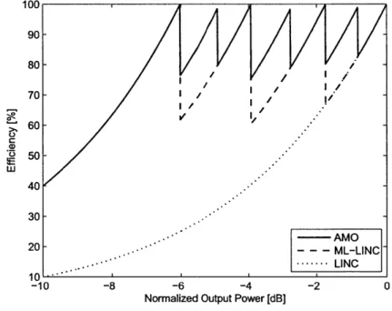
implement-ing Multi-Level LINC and the AMO architecture compared to LINC as described above. In this example we see the use of 4 different supply levels, which contribute to the creation of 4 efficiency peaks in the ML-LINC case and 7 efficiency peaks for the AMO case as predicted. The location of the efficiency peaks may be optimized by properly scaling and setting the supply voltage levels which may be done in such a manner to correlate with the desired communication protocol's power probability distribution, therefore placing the efficiency peaks at the locations where the transmitter will be operating the majority of the time thus improving the average efficiency of the overall system [7].
100 90 80 7. Ao wE 70 60 50 40 30 20 -10 ---10 -8 -6 -4 -2
Normalized Output Power [dB]
0
Figure 1-8: Ideal efficiency comparison between LINC, ML-LINC and AMO architectures
1.6 Research Contributions
Previous work has been done to show the benefits and potential improvement of average efficiency with the use of the AMO architecture in cellular frequency bands [9, 10]. In this research I will focus on the design and implementation of two of the key building blocks of this architecture - the amplitude switching network and the phase modulator.
In Chapter 2 I will present the design considerations, implementation and simulation testing of a power supply switching network for an AMO architecture operating at mm-wave frequencies. The many challenges that arise when dealing with a high carrier fre-quency of 45 GHz, accompanied by a very fast data rate will be discussed and analyzed along with various concepts to allow improvement of the linearity of the overall system.
A new technique for achieving accurate and fast phase modulation required for AMO
systems will be presented in Chapter 3. A detailed analysis of the deign considerations and theory will be presented and the results of measurements of a 65 nm test chip implementing the new design will be discussed, showing an effective 10.2 bit resolution and a settling time of less than 5 carrier cycles to within ±10. The phase modulator also complies with the spectral masks for transmitting in the Medical Implant Communication Services (MICS) band.
Chapter 2
Amplitude Modulation
2.1
Introduction
Amplitude modulation has been an integral part of communication systems since their very earliest days as a method of transmitting data. The simple methods for modulating and demodulating an amplitude of a signal helped spread its use in communication systems.
In the AMO architecture however it is important to understand that the amplitude mod-ulation we are interested in differs from this traditional view of amplitude modmod-ulation. We are not performing amplitude modulation which will directly change the transmitted sym-bol, that will be achieved via the combining of the outphased signals. The amplitude modu-lation is done to the PA power supply to enable high efficiency by minimizing the required outphasing angle at different output power levels. In this sense, our amplitude modulation resembles more a power converter rather than a traditional amplitude modulation.
It is important to understand what exactly are our requirements from the AM path. Since we are supplying the power to the PA supply, we do require it to be high power and therefore also efficient, since otherwise we will degrade the overall system efficiency due to this block. We may also require this path to be fast, comparable to the sample rate (although this demand might be relaxed a bit as we shall see later on). We do not however impose a demand on the AM block to be accurate. Unlike the polar architecture where the signal's amplitude modulation derives from the AM block and thus requires it to have a high dynamic range and resolution for adequate output levels for complex modulation
schemes [11], the AMO architecture only requires the ability to toggle amongst a few discrete predetermined levels.
This theme, not demanding to "have it all" will also appear later in Chapter 3 where we discuss the requirements from the Phase Modulator (PM) block for our system. We will see that there we will have a different set of requirements and demands, but again, we will avoid demanding that a system be simultaneously fast, accurate, high power and efficient. This relaxation in demands is what enables us to gain the important aspects of the circuits and compromise on the less critical ones towards a successful overall system design.
2.2
Power Supply Switch Network
Now that we have defined the required properties of our AM block we may more precisely define how we wish to implement and achieve these goals. In this work we will discuss the design and simulation of the power switching network built for use in an AMO ar-chitecture targeted for operation at mm-wave frequencies of 45 GHz. This project will be implemented in 45 nm Silicon On Insulator (SOI) technology. The use of SOI technology allows us to achieve higher operating frequencies for the transistors, and also opens up some possibilities in the design of the power switches as we shall shortly see. Our design utilizes 4 power supply levels - 1.1, 1.4, 1.8 and 2.2 Volts. This range was chosen to
al-low for flexibility in the output power while limiting the maximum supply level to twice the nominal supply voltage, and the difference between lowest and highest supply to one maximum nominal voltage setting.
A block diagram of the proposed power supply switch and control network is shown in
Figure 2-1. This control scheme is replicated for each PA. The 2 bit control word A,[1 : 0] (x referring to one of the two outphasing PAs) is passed through a tunable delay element controlled by a 6 bit control word Dx[5 : 0], it is then decoded, with a selection whether to
enforce switch control overlap or a dead-time period. The 4 individual switch control sig-nals are level shifted before driving the actual power switches through a slew-rate controlled driver chain. The following sections present a detailed explanation as to the importance of each circuit in the overall block, its design considerations and simulation results.
VDDi
A[:]2 2 L
Ax[1:i Decoder 2to4
|
x4 >6 SL[2:0] VOUTx
Dx[5:0]
OVLP
Figure 2-1: Power supply switching network block diagram
2.2.1
Switch Design
We shall begin our analysis from the last building block of the circuit - the power switch itself. The last stage of the pipeline needs to relay the various power supplies to the PA drain with minimum interruption manifesting as voltage drops and power loss. Since in our design we are only required to toggle amongst 4 possible power supply levels which are generated off-die, we will implement the switches as simple NMOS/PMOS devices conducting the supplies based on their control signals. All switches will be connected to their respective supply, and on their other side shorted together and connected to the PA
drain through a choking inductor.
Since the supplies themselves are constrained to the set VDDi E [1.1, 1.4,1.8,2.2] the
PA drain, denoted as VOUTX will also be a value in that range. This means that we can think of the system as operating in a shifted version of a "regular" system which would operate between ground and VDD1. We may preform this level shifting since we are using
SOI CMOS technology and the bulk node is left floating. Thus, we may use only a single
device as the switch, foregoing the need to cascade devices. We will discuss this attribute further in Section 2.2.4
Previous work has explored the switch design considerations for lower frequencies as for different fabrication processes [12]. One of the main design aspects of the switches is the choice of device type (N or P) as well as the sizing of the devices. In order to help determine the appropriate sizing, a simulation deck was constructed to mimic the operation environment of the switches. In our architecture each PA is further separated into 8
in-phase PAs in order to distribute the output power requirements over multiple blocks. The
layout of the switch blocks was done to accommodate with this topology, associating a
separate switch block with each PA slice. The simulations following were also preformed
on a single PA slice and therefore the transistor sizings correspond to one such slice.
Although from the description so far one might consider the system to be symmetrical
in respect to the various power supplies, one should keep in mind that the use of higher
power supplies correspond to a higher output power and to fewer high power symbols in
the constellation. In fact, a closer look at a typical data set, transmitting random 64-QAM
symbols oversampled by 2, reveals a very uneven distribution of use of power supplies.
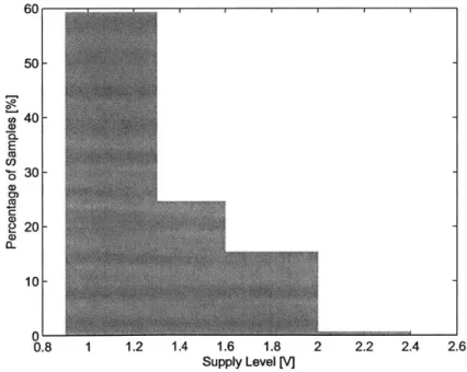
Figure 2-2 shows the frequency of use of each power supply level for an example data
set consisting of 10,000 samples. As can be seen, a vast majority of almost 60% of the
samples uses the lowest power supply, an additional
25%
use the second lowest, 15%
use one higher and a mere 0.7% use the highest supply level. It is important to keep
these numbers in mind when considering the importance and optimization of each part in
the system. We will choose to implement all switches having the same size, this may be
0 50- ca40--E CO U) 0 3 0-a. 0 0 0.8 1 1.2 1.4 1.6 1.8 2 2.2 2.4 2.6 Supply Level [V]
considered sub-optimal due to the inherent differences between NMOS and PMOS devices, but as we shall see further on, these differences are small and the advantages of simple and reusable patterned layout exceed them. We will also choose to implement the switches for the bottom two supples as completely NMOS, and the switches to the top two supplies as completely PMOS. Here the choice is a matter of preferring simple reusable layout, as well as a more simplified control scheme over pin-point optimization which is not very sensitive to these changes as we shall shortly see.
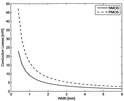
The two main sources of inefficiency and power loss in a switch are conductive losses and switching losses. Conduction loss can be accounted for by the fact that the non-ideal switch has a finite on-resistance, which therefore causes a voltage drop to form across its terminals while it is conducting current, and this loss resembles ohmic conductive losses and can be represented as
Pcond = VDSIDS
(2.1)
In a MOS transistor, the equivalent resistance is inversely proportional to the devices width, so we can expect that the conduction loss (as well as the voltage drop across the switch) will go down as the device size increases, and this is shown in the simulation result plotted in Figure 2-3 for the NMOS and PMOS switches.
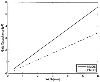
Switching losses arise due to the fact that in order to open and close the switch we must charge and discharge capacitive loads, namely the transistor's gate capacitance. The moving of charge back and forth, even through small source resistances accounts for power dissipation. The amount of charge required to charge or discharge a capacitive load C by a voltage difference AV is given by
AQ = CAV (2.2)
If we now assume that the switch is opened and closed regularly with a clock frequency
f,
and an activity factor a, representing how often the switch is typically opened and closed, e.g. opening and closing it alternatively every clock cycle will result in a maximum activity factor of a =j. We may define an effective switching current
Isw
=
4
= aCAVf (2.3)50 -- NMOS 45- --- PMOS 40-35 -E 30--j 25-0 20-0 0 15- 10-0 0 1 2 3 4 5 6 Width [mm]
Figure 2-3: Switch conduction losses
So the switching power loss can be defined as this switching current times the voltage difference used to charge and discharge the load capacitance
Ps, = IWAV = caCAV 2f (2.4)
The maximum desirable clock frequency, or sample rate, in our system is
f
= 4GHz.The voltage difference as discussed above is in our case AV = 1.1 V. The activity factor
may vary, and in the worst case is equal to half, but a more realistic value examining sample data sets suggests a typical value would be closer to a = 1. This is also reinforced by the
results shown in Figure 2-2, since if we are 60% of the time at the lowest supply level it is not possible that we would switch each and every clock cycle. The load capacitance is basically the switch total gate capacitance which we require to charge and discharge in order to open and close the switch for conduction. The gate capacitance is linearly proportional to the device width and therefore increases with the scaling of the transistor size as shown in Figure 2-4. We can see that for the NMOS devices the gate capacitance is
about 0.94 -, and about 0.57 for the PMOS devices. 3C 4 -.-C 3 NMOS -- PMOS 0 0 1 2 3 4 5 6 Width [mm]
Figure 2-4: Gate capacitance
It is clear therefore that the power loss due to switching will also be linearly proportional to the device size as shown in the simulation results plotted in Figure 2-5. Combining Eq.
(2.1) and (2.4) will give us the total power loss associated with the switch
Ptotal = Pcond+P = VDSIDS + aCAV2f (2.5)
The fact that the conduction term decreases with width while the switching term increases with width suggests that there exists an optimum point in our design where these two opposing trends balance each other. This can be seen in the plot of the total power loss for each switch plotted in Figure 2-6. We may also observe that the optimum points of the graphs are relatively shallow, and vary moderately as the device size increases.
As mentioned previously we wish to set all switches to have the same size. To do so, we should take into account the fact that the lower two supplies will be much more heavily used as seen in Figure 2-2. Therefore, plotting the total switch power loss as a weighted
7 E 0 CO 0 1 2 3 4 5 6 Width [mm]
Figure 2-5: Switch switching losses
6 3
Width [mm]
Figure 2-6: Switch total power loss
50 45 40 §735 E 0n 30 0D 0 -J 25 0 20 15 10
sum of the NMOS and PMOS switch power losses, with an 85: 15 ratio results in the power loss plot given in Figure 2-7 with a minimum point at a device width of 3.2 mm.
30 25-E 20-0 15-0) 10- -5 ' 0 1 2 3 4 5 6 Width [mm]
Figure 2-7: Switch weighted power loss
It should be noted once more that the values used for these assessments may vary, but since the optimum point is not very sensitive to change this will not affect the overall design greatly. Setting the switch device width for each PA slice in our design is the first step in designing the switch network circuit allowing us to proceed with the remaining blocks described previously. The remaining elements will come to support and provide adequate drive and timing to operate the switches as the overall system architecture requires.
2.2.2
Time Alignment
One of the most important aspects of the AMO system which must be taken into consid-eration is the time alignment between the signals of the two combining PAs, as well as the time alignment between the amplitude path and phase path for each PA on its own. The first aspect exists only in outphasing systems, while the second is true to all transmitter architectures, but is more pronounced in systems which employ a polar-style modulation. For linear transmitters using I and Q data paths, there is an inherent symmetry between the two signal routes, so symmetrical, matched layout may help greatly to reduce offsets and mismatches and align the signals. When the signal is broken down to amplitude and phase, it suffers from the fact that these two components will most likely transverse very different paths to the output, so one cannot guarantee matching and alignment by design and layout. In this case intentional, implicit time alignment blocks are necessary to make sure that each symbol arrives properly to the transmitter and that the two sides are working in unison.
To allow for such time alignment between paths, and between sides, we shall introduce into the system a controlled delay element in each of the paths (amplitude and phase) in order to allow skewing of the signal arrival time in any direction. It should be noted that it will probably be an easier task to delay and time align not the actual signals themselves after modulation, but rather the coded control signals which arrive to the individual blocks, due to their digital nature and high Signal to Noise Ratio (SNR).
We will require a control range which can span up to half of a sample period to allow complete coverage. If the mismatch between two paths is greater than half a sample period we may correct this simply by delaying the digital input by the required sample amount to reduce the mismatch to within half a sample period. It would seem this constraint will impose a minimum data rate frequency which we can operate in, however, for lower data rates with longer sample times, the relative offset between the paths becomes less signifi-cant since it is a much smaller fraction of the sample period.
To achieve the ability to delay the control signals by time periods which are smaller than the sample period implies we will not be able to do so in a digital manner, which will require a much faster clock signal to do so. Therefore we will employ an absolute
delay scheme, though it will indeed have the drawback that it does not scale with the clock frequency, but as mentioned previously, the absolute delay becomes less meaningful as the data rate decreases. The basic delay cell we will use is shown in Figure 2-8. This cell allows to choose whether the signal shall pass through a direct path or through a capacitively loaded buffered path, which will relatively delay it. The size of the loading capacitor will determine the amount of delay time each cell creates, and by binary weighting these cells and cascading them we are able to create a controlled delay element.
IN OUT
>T
Figure 2-8: Delay cell element
The resolution of our delay cell will be determined by the smallest capacitor value in the chain and the dynamic range will be set by the number of bits, or binary scaled cells used in the delay chain. For our design, targeting a data rate of 1 - 4GHz we will scale the chain so as to allow a maximum delay of up to roughly 500ps and a resolution of roughly 5ps. This would seem to imply a size of 7 bits for control of the chain, but since the direct path itself has a finite minimum delay it is sufficient to use 6 bits for control. This delay is achieved by a use of a 10 fF capacitor size for the Least Significant Bit (LSB).
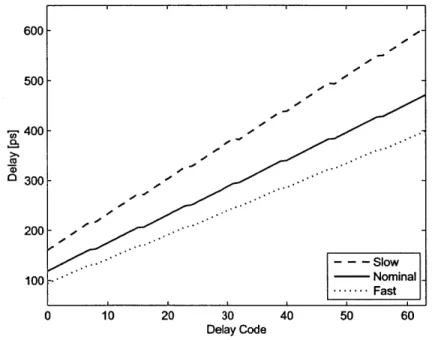
Since this delay cell creates delays which are absolute and dependent on capacitive loading and the driving strengths of the buffers propagating the control signals it is im-portant to consider the effects of variations caused due to changes in Process, Voltage and Temperature (PVT). The cell will produce the longest delay, i.e. operate at the slowest corner, when the process is at the slow comer, the voltage is at the lower range of values and the temperature is high. Conversely, the cell will exhibit the shortest delay and fastest operation when the process is fast, the voltage high and the temperature low. Figure 2-9
illustrates this via a corner simulation of a code sweep of the delay cell, measuring the
delay of a test signal propagating through. The nominal values were taken to be at
27
C
and a supply voltage of 1 V. The slow corner was simulated with the temperature at
1000
C
and
VDD =0.9V and the fast corner was set at 0 C and a supply voltage of 1.1 V.
600- -500 -400 00 200-- 200-- 200-- Slow 100 -Nominal --- Fast 0 10 20 30 40 50 60 Delay Code
Figure 2-9: PVT corner simulation of delay cell
2.2.2.1 Nulling Test
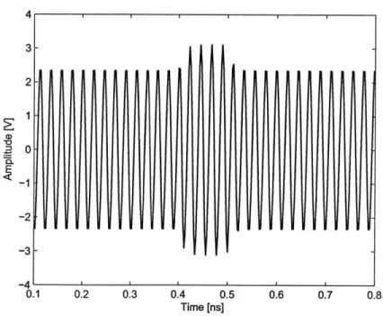
An extremely important aspect (albeit sometimes overlooked) of being able to control, trim and program various components and blocks in a system is the ability to test it and de-vise a scheme to enable the proper setting of the component. An extensive and flexible programmable device is still worthless if one cannot define a way to determine how it should be set. In our system, as described earlier, there are two main time alignments to be concerned with - time alignment between the phase and amplitude paths and alignment between the two outphasing PAs. Our chosen architecture of Asymmetric Multilevel Out-phasing opens up the possibility to determine the correct timing alignment in interesting ways.
For both cases we will employ a similar concept - "Nulling" tests, i.e. experiments where the outcome should be null, or have minimal effect. This can be achieved in general in a system which is non-injective, so as to have two or more states which will yield the same outcome. In our case, to determine the proper timing between the two outphasing PAs we may subject a test where the amplitude is initially set different for the two sides, than simultaneously swap, so
al (t2) = a2(ti) and a2(t2) = al (ti) where a (ti)
#
a2(tl) (2.6)Due to the symmetry of the system the output should ideally remain unchanged, there-fore any misalignment of the timing paths between the two sides will pronounce itself via perturbations to the combined output resulting in a momentary change in amplitude or a degradation of the noise floor of the output spectrum. An example of this is shown in Fig-ure 2-10. This will determine the relative timing offset between the two outphasing sides.
0.2 0.3 0.4 0
Time [ns]
.5 0.6 0.7 0.8
Figure 2-10: Amplitude path misalignment of 100ps
4 3 2 1 0 0, CD -1 -2 -3 -4 t 0.1
Similarly, due to the fact that our system employs several levels of possible supply
voltages there is more than one set of phase and amplitude which will yield a given output.
This fact enabled us to switch to a lower amplitude with a smaller outphasing angle in order
to improve average efficiency and it will also enable us to determine the timing alignment
between the phase and amplitude paths. Again we set an experiment where now, after the
two sides are aligned, we switch the amplitude and phase values while still ideally obtaining
the same output value. Any misalignment will again manifest itself in a disturbance of the
amplitude and phase of the combined output waveform.
In both alignment cases we may not be able to achieve an ideal result, but this scheme
does provide a way to achieve the best result by minimizing the output disturbance and the
signal spectrum's noise floor.
2.2.3
Decoding and Overlap Control
The control signals arriving to the switches are sent binary coded and therefore need to be
decoded before the actual commands are passed through to open and close the appropriate
switches. The decoding process is straight forward, and done via a simple digital 2-to-4
decoder as shown in Figure 2-11. At each given time point only one switch control signal
should be high, corresponding to the desired PA supply voltage.
A[1] A[O]
Cti[O]
Ctr1[1]
ctrI[2]
ctr1[3]
Figure 2-11: 2-to-4 Decoder
Special attention should be given to the transition between any two supply levels, i.e.
the switch control transition hand-off from one control to the other. Ideally this transition
would occur instantly, where one control goes down in zero time, the other goes up si-multaneously in zero time. Of course, this is not a realistic model of the control signals. The drivers have finite rise and fall times therefore we are guaranteed to have either an overlap between two signals during transition, or a dead-time where no switch is on. An overlap between the signals will cause a short period of time where two supplies are ba-sically shorted together, and so a shunting current will flow from one to the other through the switches causing power losses and efficiency degradation. On the other hand, a dead time, will cause an intermittent droop in the voltage supplied to the PA degrading the sym-bol output and spectrum. The amount of power loss or voltage drop is dependent on the transition time, the switch resistances and the capacitance on the supply node.
In order to allow for maximum system flexibility and allow for different trade-offs in the digital pre-distortion block, a mechanism was introduced to ensure either a guaranteed short overlap of control signals or a guaranteed non-overlap. This is achieved using the simple circuit depicted in Figure 2-12(a). The AND gate with the delayed input ensures that the output will have a delayed rise compared to its input, this is suited to the case where we wish there to be no overlap, if we invert the polarity of the signal before and after the delayed AND buffer it will effectively result in a signal with a delayed falling edge, which is suitable for use in the case where we do desire an overlap. The inversion of polarity is easily achieved by the XOR gates at the input and output, where the other leg is connected to a signal indicating the desired state (low for no overlap and high for overlap). An illustration of the signal timings is presented in Figure 2-12(b).
Ctrl[ij] _ [ ~ ~
-1
C t r L o V [ i ] O V i
j]-Lizi1
iz..V
CtrI OV[i,j]
EZZLE
J
---
i-(a) Schematic (b) Timing diagram
Figure 2-12: Overlap control scheme
As before it is crucial to verify that the desired behavior of our block remains consistent across variations in PVT. Therefore a comprehensive sweep was preformed in simulation to measure the amount of overlap (as a positive time value) or non-overlap (as a negative
time value) as a function of every possible transition between two power supply levels and across several PVT conditions. The results shown in Figure 2-13 demonstrate that the design assures us that the block will function as expected under all of these various
scenarios.
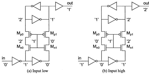
2.2.4 Level Shifting
As discussed earlier, the choice to use thin gate FETs enables us to operate at higher speeds but poses severe limitations on the voltage which can be sustained across the device's ter-minals. This limitation is even more pronounced in our deep sub-micron process where the voltage across any 2 terminals should not exceed roughly 1.1 V. The use of SOI technology though, removes this concern regarding the bulk node, so unlike Bulk CMOS we can use the devices between higher voltages, so long as the difference between any two terminals is less than the maximum allowed and we are not constrained to have all bulk nodes tied to one common voltage level. Therefore we may use the switch devices between the power supplies and the PA drain without the need to cascode it as long as we keep the difference between the maximum supply to the lowest one to be below 1.1 V, as it is in our case.
This operating scheme requires however that we use some sort of level shifting for the switch control signals in order to provide adequate over-drive to the transistors. In our design, since the supplies and PA drain will always vary between VDD1 = 1.1 V and
VDD4 = 2.2V we may obtain proper overdrive of the switches by transitioning the driver
signal from their usual domain between ground and VDDI to a shifted domain between VDD1
and VDD4. This is achieved via a level shifter topology [13] shown in Figure 2-14. In this
topology the bottom inverters and the input operate at the lower voltage domain, between ground and VDD1, the top inverters operate at the higher voltages and the cascoding middle devices ensure the separation between the two domains and relieve the stress on the devices when transitioning from one domain to the other.
For simplicity, let us define the ground voltage as '0', the lowest supply as '1' and the maximum supply as '2', such that we require that each device has a differential voltage no greater than '1' across its various terminals. We may understand the operation of this level
-15 E I-0. Co a) 0 Transition
(a) Without overlap
*L 35 30- >25-0. 20 - - 15-Slow 10- Nominal -- ..- Fast 5' 0-->10-->20-->31 -->01-->21-->32-->02-->12-->33-->03-->13-->2 Transition
(b) With overlap
out
'1'
'2'
'1'
MPO
'2'
MnOin
'0' M Mn1out
'2'
'1'
'2'
MPo'0'
Mao M1'2'
Mn1in
(a) Input low (b) Input
high
Figure 2-14: Level shifter schematic
shifter by following the signal change path from input to output. For a signal at the input which goes from a low '0', to a high '1', the bottom inverter outputs change accordingly. The bottom NMOS transistors (Mo and Mni) begin conducting. Mno starts discharging the middle node bringing it to '0', MnI begins charging the middle node to '1' (although it will do so only up until a threshold voltage below that). At this point only the left hand side PMOS, Mpo will be open and begin discharging the left node. Since Mpi is closed, the discharging may overcome the back-to-back inverter "memory" and flip its state, at that point Mp1 will open and charge the right middle node to '2' and the output buffer will
propagate the change in the output from '1' to '2' and the transition is complete.
Similarly, going from a high '1' to low '0' at the input will first open the two bottom
NMOS devices, but this time it will charge the left middle node and discharge the right
middle node. At this point the open right PMOS, Mp1 will allow the discharge of the right
half of the inverter loop, causing them to flip and change the output from a high '2' to a low '1'. Again ensuring throughout the entire procedure that no device encounters a differential voltage greater than one supply level between any of its terminals.
2.2.5
Slew Rate Control
The driver stage preceding the power switches are responsible for providing adequate drive strength in order to open and close the switches at a reasonable rate. In this section we will review how varying the driver strength affects the switch and output rise and fall times and how this may serve us in the overall system output shaping.
To analyze the effects of varying rise time of the output supply amplitude, we will make a few simplifying assumptions. Let us consider a scenario (which is actually very pessimistic according to our discussion so far) that we wish to toggle the output between the lowest and highest supply at the maximum data rate. In this case, the output will take the form of a periodic square wave function, which we can normalize to a magnitude of 1, with pulses of width ts, the data rate, and period T = 2ts. This waveform can be expressed as 1 t< 'ts
f(t)
= (2.7) 0 else Where also f(t+nT)=f(t) VnEZ (2.8)For this waveform, the corresponding frequency domain Fourier series is
F(on) = tssinc tson
ts n = 0
= tssinc n =
{
0 n even (2.9)(-1)n+1
n
oddThe finite rise time of the output square wave may be modeled as a linear slope. This is of course not accurate, but close and will allow us to conduct rough simplified calculations and analysis. The finite rise time tr, can be generated in our waveform as a convolution of the original ideal square wave with an additional periodical square wave with width tr and
height -as seen in Figure 2-15. Expressed as an equation this resolves to
g(t) =
f(t)*
-f
t
(2.10)tr \tr/
-2 /2 2 2
Figure 2-15: Linear slope as convolution of two square waves
The Fourier series corresponding to this finite rise time waveform will therefore be
1
tr (trG(con)= F((on) -tr ts I rF con-tts
= tssme -Cn smec --trn (2.11)
(2 ) 2 ts
This result implies that there is an added attenuation of the original square wave odd har-monics due to the finite slope by an additional sinc filter. The amount of added attenuation to each harmonic grows with the harmonic number as well as with the ratio of rise time to sample period -. The attenuation of course is less significant for higher harmonics which were lower to begin with. A plot of the added attenuation for several low order harmonics for different slope percentages is shown in Figure 2-16.
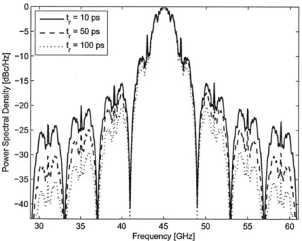
The affects of varying slopes were simulated on an ideal model of the system with only amplitude switching to emphasize the effect. These results are shown in Figure 2-17 for rise times of 10, 50 and 100ps which correspond to a slope ratio of 4%, 20% and 40% respectively for a sample period of 4GHz. The attenuation of the higher order harmonics can be seen in the plot. This attenuation occurs outside the symbol frequency band, so it does not help to shape the spectrum, but it does imply a reduced requirement on the external filters used after the transmitter to limit the output outside the frequency band of interest.
0.2 0.4 0.6
Slope Ratio [tr/t,]
0.8 1
Figure 2-16: Added attenuation due to varying slopes
30 35 40 45 50 55 60
Frequency [GHz]
Figure 2-17: Output spectrum for various rise times
40 35 30 25 20 15 10 5 0 C ---- n=1 --n=5 - -- -' - -' - -- -n' 0 0 M -0 cI
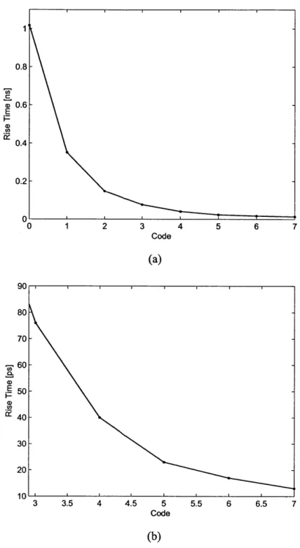
In order to achieve this possible control over the switch slope, the driver stage was designed as a tri-state buffer where the number of active scaled buffers could be controlled. This does not give very accurate control over the output slope but does allow for some flexibility in the choice of the final slope rise time. Figure 2-18 plots the simulated rise
time of the switch output given the different 3-bit control word.
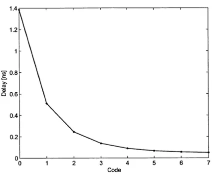
An artifact of the increased rise time is also an increase in absolute delay of the circuit from the moment the control word changes until the output is modified as shown in Figure
2-19. However this delay is relatively fixed and can be canceled out using the same
tech-niques described in Section 2.2.2 once the desired slope is selected for use in the system.
Figure 2-18 also reveals that the lowest code values create rise times which are in a time scale larger than our maximum designed data rate, meaning that they are impractical to use for the extreme speed case. There is however still merit in using them when going to lower data rates, or for an alternative slewing scheme where we intentionally set the am-plitude switching to be slower than a sample period. In such a scenario, we may relax the requirements on the power switching network such that it is not required to toggle at the full sample rate, but perhaps change in a more relaxed rate, say every 5 or 10 sample periods. This relaxation will greatly reduce requirements on the block and its power consumption. We do however require in this case to compensate for the degraded control of amplitude
by our still fast control of the phase. As long as the transitions from one amplitude level
to another are systematic and predictable, we can compensate for the inaccurate amplitude transition time by correctly pre-defining a correction to the phase values during such tran-sitions. These corrections require of course more digital-intense background calculation and lookup tables but may still be worth the effort given the relaxed demands on the high power switches.
0.81 e 0.6-E a) 0.4- 0.2-0' 0 1 2 3 4 5 6 7 Code (a) 90 80 70- 60-a. 50- i-a) i 40- 30- 20-10 3 3.5 4 4.5 5 5.5 6 6.5 7 Code (b)
'- 0 0.8-0 0.8-0.6 - 0.4- 0.2-0' 0 1 2 3 4 5 6 7 Code
Figure 2-19: Static delay caused by slew rate control
2.3
Summary
The design and analysis of a power switching network for an Asymmetric Multilevel Out-phasing transmitter was presented. The power switching network was designed to toggle at a maximum sample rate of 4 GS/s between 4 discrete power supplies to provide sufficient current to the outphasing PAs. Use of the SOI process technology enabled to use level shift-ing to reduce the number of devices and increase circuit speed without neglectshift-ing reliability and breakdown considerations. The switch control scheme was planned with a high degree of flexibility allowing to control overlap of control signals and their timing for alignment between the different amplitude and phase paths, as well as output slew rate in order to allow more degrees of freedom in the system to trade off performance and efficiency.
The proposed design was implemented and fabricated in an IBM 45nm SOI process,
as part of a complete AMO transmitter architecture. The test chip is currently back in the lab for testing and measurement results should follow in the coming months to demonstrate many of the aspects discussed in this work.