HAL Id: hal-03026860
https://hal.archives-ouvertes.fr/hal-03026860
Submitted on 11 Dec 2020
HAL is a multi-disciplinary open access
archive for the deposit and dissemination of sci-entific research documents, whether they are pub-lished or not. The documents may come from teaching and research institutions in France or abroad, or from public or private research centers.
L’archive ouverte pluridisciplinaire HAL, est destinée au dépôt et à la diffusion de documents scientifiques de niveau recherche, publiés ou non, émanant des établissements d’enseignement et de recherche français ou étrangers, des laboratoires publics ou privés.
Nanoparticles growth in dusty plasmas from
organosilicon precursor
Y Fermi, Salah Sahli, M. Kihel, S Mouissat, P. Raynaud
To cite this version:
Y Fermi, Salah Sahli, M. Kihel, S Mouissat, P. Raynaud. Nanoparticles growth in dusty plasmas from organosilicon precursor. Fifth International Conference on Energy, Materials, Applied Energetics and Pollution. ICEMAEP 2019, Oct 2019, Constantine, Algeria. pp.1649. �hal-03026860�
1649
Fifth International Conference on Energy, Materials, Applied Energetics and Pollution. ICEMAEP2019, October22-24, 2019, Constantine, Algeria.
M.KADJA, A. MEHEL, A.ZAATRI, H.CHEMANI, S.BENISSAAD and K. TALBI (Editors.).
NANOPARTICLES GROWTH IN DUSTY PLASMAS
FROM
ORGANOSILICON PRECURSOR
Y. FERMI1, S. SAHLI1, M. KIHEL1, S. MOUISSAT1, P. RAYNAUD2 1
Université Frères Mentouri Constantine 1, Laboratoire Microsystèmes et Instrumentation (LMI), Algérie, Route de Ain El Bey, 25017 Constantine- Alegria.
2
University Paul Sabatier, Laboratory of Plasmas and Energy Conversion (LAPLACE), 118 Route de Narbonne, 31062 Toulouse CEDEX – France.
ABSTRACT
In this work, plasma discharge has been generated from pure HMDSO precursor in low frequency reactor. It has been observed that a cloud of Nanoparticles could be formed in a plasma discharge for some deposition parameters such as discharge power, time and pressure. Discharge signal analysis have been used in order to investigate the effect of deposition parameters on the nanoparticles growth. The study of discharge signal analysis shows that the pulse frequency is strongly related to plasma composition. Their value shifted from about 170 Hz to 250 Hz according to deposited parameters. This shift has been attributed to the nanoparticles formation in the plasma reactor. On the other hand, Nanoparticles embedded in thin films have been characterized by EDX and FTIR spectroscopy in order to reveal the NP’s composition.
Key Words: Nanopowders, Dust, growth mechanism, PECVD
NOMENCLATURE
Symbols : Abbreviations:
Fp Pulse Frequency, Hz HMDSO Hexamythildisiloxane P pressure, mbarr NPs Nanoparticles
1. INTRODUCTION
Since the first observation of Nanoparticles, they were considered as harmful or impurities in microelectronics technology. In previous works1, Nanoparticles (NPs) have been observed encapsulated in thin layers, the chemically active species allow to grow particles or to modify their surface properties2, which leads to form new materials. However, the fact that plasma process mechanism leads to powder formation in plasma discharge is not yet fully investigated. Many studies were made in order to better understand the mechanism of nanoparticles formation in plasma discharge. In this paper, a study based on plasma enhanced chemical vapor deposition (PECVD) as a deposition technique and Hexamethyldisiloxane (HMDSO)as precursor is conducted using discharge signal analysis in order to find the best conditions to create NPs. To gain more information about the composition of new material (NPs) an Energy Dispersive X-ray spectroscopy analysis were made.
2. EXPERIMENTAL METHOD
2.1 Creation of particles in dusty plasma:
The plasma discharge was generated using a pulsed wave generator that has a power range from [6 – 26] W and a wave frequency of 33 KHz. The pressure of HMDSO vapor has been varied in the range of [0.2 - 1] mbar. Moreover, deposited time has been varied from 2 to20 min. The plasma polymerized thin layers were
deposited on intrinsic silicon. Fig.1 presents the PECVD reactor used in this study. it is described in a more detailed way elsewhere 1.
FIGURE 2.2 Film Characterization
The pulse frequency is monitoring using Tektronix TDS2024C and a high voltage probe
variation of this parameter is used in order to investigate the discharge signal analysis during plasma discharge. Chemical structure and composition of deposited thin layers were characterized by means of FTIR spectroscopy using a Thermo Nic
morphological feature of the coated film, scanning electron microscopy (JEOL JMS
3.1 Discharge Signal Analysis:
The applied signal used to generate plasma
and wave signal. it is more described in Fig2a). This figure shows theoretical signal delivered by generator. The pulse frequency is considered as the envelope frequency (it is represe
wave frequency is the applied signal frequency (it is represented in a blue line).
1650
deposited on intrinsic silicon. Fig.1 presents the PECVD reactor used in this study. it is described in a more
IGURE 1:DESCRIPTION SCHEMATIC OF THE EXPERIMENT
The pulse frequency is monitoring using Tektronix TDS2024C and a high voltage probe
variation of this parameter is used in order to investigate the discharge signal analysis during plasma discharge. Chemical structure and composition of deposited thin layers were characterized by means of FTIR spectroscopy using a Thermo Nicolet Avatar 360 spectrometer. To characterize the evolution of the surface
of the coated film, scanning electron microscopy (JEOL JMS-7800F
3. RESULTS
Discharge Signal Analysis:
The applied signal used to generate plasma discharge is composed of two types of signals; pulse signal and wave signal. it is more described in Fig2a). This figure shows theoretical signal delivered by
The pulse frequency is considered as the envelope frequency (it is represented by green line) and the wave frequency is the applied signal frequency (it is represented in a blue line).
deposited on intrinsic silicon. Fig.1 presents the PECVD reactor used in this study. it is described in a more
The pulse frequency is monitoring using Tektronix TDS2024C and a high voltage probe (P6015A). The variation of this parameter is used in order to investigate the discharge signal analysis during plasma discharge. Chemical structure and composition of deposited thin layers were characterized by means of FTIR To characterize the evolution of the surface
7800F) has been used.
discharge is composed of two types of signals; pulse signal and wave signal. it is more described in Fig2a). This figure shows theoretical signal delivered by pulsed wave nted by green line) and the
FIGURE 2: A)THEORETICAL PULSED -100 130 135 140 145 150 176 192 208 224 -100 30,8 33,0 35,2 37,4 Fre quenc y (Hz ) Frequ e nc y (KHz)
FIGURE 3:PULSE FREQUENCY
Fig.3 shows both frequencies’ (pulse and wave frequency) value evolution as a function of different depositions parameters. It can be observed that wave frequency remained constant with fw=33 kHz, which is the set value used in this experiment. Whereas for the measured pulse frequency
parameters, it have been observed that fp value is strongly
increases for high power discharge 26 W and decreases for low power discharge 6 layer is represented with a parallel RC, the resonance frequency of such circuit is:
frequency is the resonance frequency of the discharge. It explains the increase of pulse frequency at high applied power by the decrease of the impedance due to the high fragmentation of the gas in plasma. However, pulse frequency decreases when the impedance increases at low applied power due to the low fragmentation. At dusty plasma which is related to the presence of nanoparticles, the discharge seems to be more resistive. Also, the primary species of the nanoparticles tend to have negative
charged in order to accumulate3. This property implicates the use of nanoparticles impedance that is pa
the plasma impedance.In Fig.4 A), the pulse frequency at 6.5 W seems to be constant during plasma discharge. While it changes with the increase of pressure in the plasma reactor. The rising of pressure leads to high impedance values which cause low pulse frequency.
A)
1651
ULSED WAVE SIGNAL, B)EXPERIMENTAL PULSED WAVE APPLIED
-100 0 100 200 300 400 500 600 -100 0 100 200 300 400 500 600 Time (Sec) Pulse Frequency (6,5 W) Pulse frequency (26 W) Wave frequency
REQUENCY VARIATION DURING DEPOSITION OF THIN FILM (0.4
Fig.3 shows both frequencies’ (pulse and wave frequency) value evolution as a function of different rs. It can be observed that wave frequency remained constant with fw=33 kHz, which is the set value used in this experiment. Whereas for the measured pulse frequency ( )as function of depositions parameters, it have been observed that fp value is strongly linked to deposited parameters. We notice that fp increases for high power discharge 26 W and decreases for low power discharge 6
layer is represented with a parallel RC, the resonance frequency of such circuit is:
frequency is the resonance frequency of the discharge. It explains the increase of pulse frequency at high applied power by the decrease of the impedance due to the high fragmentation of the gas in plasma. However,
hen the impedance increases at low applied power due to the low fragmentation. At dusty plasma which is related to the presence of nanoparticles, the discharge seems to be more resistive. Also, the primary species of the nanoparticles tend to have negative ion properties because they must be
. This property implicates the use of nanoparticles impedance that is pa
), the pulse frequency at 6.5 W seems to be constant during plasma discharge. e increase of pressure in the plasma reactor. The rising of pressure leads to high impedance values which cause low pulse frequency.
B)
AVE APPLIED SIGNAL.
(0.4 MBAR,10 MIN) Fig.3 shows both frequencies’ (pulse and wave frequency) value evolution as a function of different
rs. It can be observed that wave frequency remained constant with fw=33 kHz, which is ( )as function of depositions linked to deposited parameters. We notice that fp increases for high power discharge 26 W and decreases for low power discharge 6,5 W.The deposited thin layer is represented with a parallel RC, the resonance frequency of such circuit is: = So the pulse frequency is the resonance frequency of the discharge. It explains the increase of pulse frequency at high applied power by the decrease of the impedance due to the high fragmentation of the gas in plasma. However,
hen the impedance increases at low applied power due to the low fragmentation. At dusty plasma which is related to the presence of nanoparticles, the discharge seems to be more resistive.
ion properties because they must be . This property implicates the use of nanoparticles impedance that is parallel to ), the pulse frequency at 6.5 W seems to be constant during plasma discharge. e increase of pressure in the plasma reactor. The rising of pressure leads to high
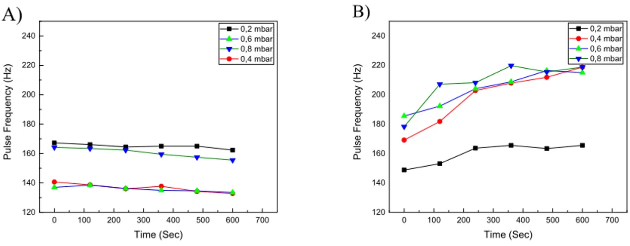
1652 0 100 200 300 400 500 600 700 120 140 160 180 200 220 240 Pu ls e Frequenc y (Hz) Time (Sec) 0,2 mbar 0,6 mbar 0,8 mbar 0,4 mbar
A)
0 100 200 300 400 500 600 700 120 140 160 180 200 220 240 Pu ls e Frequenc y (Hz) Time (Sec) 0,2 mbar 0,4 mbar 0,6 mbar 0,8 mbar B)FIGURE 4:PULSE FREQUENCY VARIATION FOR 10 MIN, A) 6.5 W. B)26W.
On the other hand, following Fig.4B), pulse frequency increases from 175 Hz to 220 Hz beyond pressure of about0.4 mbar. The shift of pulse frequency towards a value of about 220 Hz is observed for all conditions that Nanoparticles appear in the plasma discharge (dusty plasma). Therefore, from the discharge signal analysis it can be suggested that pulse frequency value variation may indicate the formation of NP’s in plasma discharge. 3.2 FTIR analysis:
Figure 5 shows the infrared spectra of films for two different deposition time: 2 and 20 minutes. The wavenumber of the main absorption bandswere collected and identified in Table 14,5. The spectra revealed the presenceof asymmetric stretching vibrations (2969 cm–1). groups of Methylsilil at 1515 cm–1 (asymmetric deformationof CH3 in (Si(CH3)x), around 1268 cm–1 (symmetricdeformation of CH3 in Si(CH3)x). Presence of Si‑O‑Sigroups around 1080-1020 cm–1 which is characteristic of the original organosiliconcompound ((CH3)3-Si-O-Si-(CH3)3).The presence of SiH (2238 cm-1) it’s formation is explained by multiple step reactions in the plasma phase4. Small amount of C=O is observed in films with a deposition time of 20 mins, this also explained by the total fragmentation of the original organosilicon molecule. Between the two samples 2 and 20 mins the last have a surface covered with powder, and we have mention in recent work that SiH molecule is a sign of powder creation6. The absence of SiH is linked with the absence of powder (nanoparticles or dusty plasma) in samples of deposition time of 2 mins. Next we intend to know the composition of these nanoparticles. 4000 3500 3000 2500 2000 1500 1000 500 0,00 0,02 0,04 0,06 0,08 0,10 0,12 0,14 0,16 0,18 0,20 0,22 0,24 0,26 0,28 SiOH HSiO Str CH3 Rot CH3 Asy CH3 Sy CH3 SiH CHx SiOH A b s o rb a n c e ( a .u )) Wavenumber (cm-1 ) 2 min 20 min Si-O-Si C=O
1653
Wavenumber (cm-1) Mode
3727.7 OH stretching in free SiOH 3315 OH stretching in free SiOH 2969.8 C-H asymmetric stretching in CH3
2308.3 C=O
2238.95 Si-H stretching
1828.1 C=O
1515.7 CH3 asymmetric deformation in Si(CH3)x 1268.9 CH3 symmetric deformation in Si(CH3)x 1080 – 1020 Si-O asymmetric stretching in Si-O-Si 898.66 HSiO hybrid vibrations
846.59 -CH3 rotation in Si-(CH3)3 [Si-C]
798.38 -CH3 stretching in Si-(CH3)2 and Si-O in stretching Si-O-Si
TABLE 1:ABSORPTION BANDS DETECTED IN THE INFRARED SPECTRA OF PLASMA-POLYMERIZED FILMS FROM PURE HMDSO
3.3 EDX analysis:
FIGURE 6:A)SEMMICROGRAPHFORNANOPARTICLES(26W,0.2MBAR,10MIN),B)ANDC)EDX SPECTRUMOFTHESURFACEANDOFTHENPSRESPECTIVELY.
a)
b)
c)
0.00 1.00 2.00 3.00 4.00 5.00 6.00 7.00 8.00 9.00 10.00 keV 001 0 8000 16000 24000 32000 40000 48000 56000 64000 C o u n ts C-K O-K Si-K Au-M Au-M Au-MAu-M Au-L Au-L
0.00 1.00 2.00 3.00 4.00 5.00 6.00 7.00 8.00 9.00 10.00 keV 0 15000 30000 45000 60000 75000 90000 105000 120000 C o u n ts C-K O-K Si-K Au-M Au-M Au-M Au-M Au-L Au-L
1654
The composition of the thin layer produced is definitely formed of carbon, Hydrogen, Oxygen and silicon according to the precursor we used (HMDSO); the nanoparticles has the same composition. An EDX analysis was made to confirm the composition of the surface in the presence of NPs and on the NPs themselves, Fig. 6 a) represent the surface with nanoparticles where the first EDX spectrum is made (B) and the point (001) on nanoparticles is where the second EDX spectrum is made (C), the amount of Si decreases in NPs (29.13 %) compared to the amount of Si in all surface (58.58 %), it may be explained by using a silicon substrate. The amount of C (29.81 %) and O (21.76 %) increases in nanoparticles compared to the amount of C (20.02 %) and O (11.10 %) in all surface.
4. CONCLUSIONS
In this work we have investigated the Nanoparticles growth process in the plasma discharge according to some deposition parameters. First we determined the best parameters to create nanoparticles based on the pulsed frequency of the discharge signal. It has been observed that the pulsed frequency is highly linked to plasma composition, also these last is related to plasma impedance. The formation of NP’s in the plasma leads to the shift of pulse frequency from 170 Hz to [215 – 235] Hz. Finally, using EDX analysis to know the nanoparticles composition, the results reveal that nanoparticles contain more oxygen and carbon molecules and less silicon molecules compared to the composition of the thin layer.
REFERENCES
[1] Nouicer, I., Sahli, S., Kihel, M., Ziari, Z., Bellel, A., and Raynaud, P. (2015) Superhydrophobic surface produced on polyimide and silicon by plasma enhanced chemical vapour deposition from hexamethyldisiloxane precursor, International Journal of Nanotechnology12, 597-607.
[2] Melzer, A. (2019) Dusty Plasmas and Magnetic Fields, In Physics of Dusty Plasmas, pp 161-170, Springer. [3] Bouchoule, A., Plain, A., Boufendi, L., Blondeau, J. P., and Laure, C. (1991) Particle generation and
behavior in a silane‐argon low‐pressure discharge under continuous or pulsed radio‐frequency excitation, Journal of applied physics70, 1991-2000.
[4] Mascagni, D. B. T., Souza, M. E. P. d., Freire, C. M. d. A., Silva, S. L., Rangel, R. d. C. C., Cruz, N. C. d., and Rangel, E. C. (2014) Corrosion resistance of 2024 aluminum alloy coated with plasma deposited aC: H: Si: O films, Materials Research17, 1449-1465.
[5] Fanelli, F., Lovascio, S., d'Agostino, R., Arefi‐Khonsari, F., and Fracassi, F. (2010) Ar/HMDSO/O2 Fed Atmospheric Pressure DBDs: Thin Film Deposition and GC‐MS Investigation of By‐Products, Plasma
Processes and Polymers7, 535-543.
[6] Fermi, Y., Kihel, M., Sahli, S., and Raynaud, P. (2019) Synthesis of nanopowders in a PECVD reactor from organosilicon precursor, Phosphorus, Sulfur, and Silicon and the Related Elements, 1-5.
![[PDF] Apprendre ALM cours en pdf | Formation Informatique](data:image/gif;base64,R0lGODlhAQABAIAAAP///wAAACH5BAEAAAAALAAAAAABAAEAAAICRAEAOw==)