HAL Id: hal-02352199
https://hal.archives-ouvertes.fr/hal-02352199
Submitted on 17 Jan 2020
HAL is a multi-disciplinary open access
archive for the deposit and dissemination of
sci-entific research documents, whether they are
pub-lished or not. The documents may come from
teaching and research institutions in France or
abroad, or from public or private research centers.
L’archive ouverte pluridisciplinaire HAL, est
destinée au dépôt et à la diffusion de documents
scientifiques de niveau recherche, publiés ou non,
émanant des établissements d’enseignement et de
recherche français ou étrangers, des laboratoires
publics ou privés.
environments
Cécile Floer, Sami Hage-Ali, Pascal Nicolay, Hugo Chambon, Sergei Zhgoon,
Alexander Shvetsov, Jérémy Streque, Hamid M’Jahed, Omar Elmazria
To cite this version:
Cécile Floer, Sami Hage-Ali, Pascal Nicolay, Hugo Chambon, Sergei Zhgoon, et al.. SAW RFID
devices using connected IDTs as an alternative to conventional reflectors for harsh environments.
IEEE Transactions on Ultrasonics, Ferroelectrics and Frequency Control, Institute of Electrical and
Electronics Engineers, 2020, Volume: 67 (6), pp.1267 - 1274. �10.1109/TUFFC.2019.2943310�.
�hal-02352199�
Abstract—Remote interrogation of surface acoustic wave
ID-tags imposes a high signal amplitude which is related to a high coupling coefficient value (K2) and low propagation losses (α). In this paper, we propose and discuss an alternative configuration to the standard one. Here, we replaced the conventional configuration, i.e. one interdigital transducer (IDT) and several reflectors, by a series of electrically connected IDTs. The goal is to increase the amplitude of the detected signal using direct transmission between IDTs instead of the reflection from passive reflectors. This concept can therefore increase the interrogation scope of ID-tags made on conventional substrate with high K2 value. Moreover, it can also be extended to suitable substrates for harsh environments such as high temperature environments: the materials used exhibit limited performances (low K2 value and relatively high propagation losses) and are therefore rarely used for identification applications. The concept was first tested and validated using the lithium niobate 128°Y-X cut substrate, which is commonly used in ID-tags. A good agreement between experimental and numerical results was obtained for the promising concept of connected IDTs. The interesting features of the structure were also validated using a langasite substrate, which is well-known to operate at very high temperatures. Performances of both substrates (lithium niobate and langasite) were tested with an in-situ RF characterization up to 600°C. Unexpected results regarding the resilience of devices based on congruent lithium niobate were obtained.
Index Terms—high temperature, lithium niobate, radio
frequency identification (RFID), surface acoustic wave (SAW) I. INTRODUCTION
HIS paper is an extended version of the conference paper [1] presented at the 2019 Joint Conference of the International Frequency Control Symposium and the European Frequency and Time Forum in Orlando, USA.
In modern society, the remote sensing of physical parameters becomes essential, as well as the remote identification of the
This work was supported by Direction Générale de l’Armement (DGA), the ANR project “SAWGOOD” (ANR-18-CE42-0004-01), the ANR project “SALSA” (ANR-15-CE08-0015-05), the French PIA project “Lorraine Université d’Excellence” (ANR-15-IDEX-04-LUE), the CPER Mat-DS, the Ministry of Science and Education of Russian Federation 8.6108.2017/6.7 and by the COMET K1 centre ASSIC.
C. Floer is the corresponding author (e-mail: cecile.floer@univ-lorraine.fr).
sensors, especially for tracking applications. Standard RFID technology is based on silicon integrated circuit (IC tags), which can be interrogated over large distances. These devices already have numerous applications in logistics and production lines monitoring. One of the major limitations of this technology is the need of initial RF power conversion to DC power, to read the devices [2]. Surface acoustic wave (SAW) ID-tags (like in Fig. 1) are another solution. The growing trend of the SAW market, and more precisely of the coding principle, was already mentioned twenty years ago [3,4]. SAW devices have the advantage of being totally passive. Moreover, these devices consist only of a piezoelectric substrate with metallic IDTs on top of it. The reverse and direct piezoelectric effects are used to convert electromagnetic signals into surface acoustic waves, and vice versa. External parameters such as temperature [5], strain or the presence of gas can disturb the wave propagation. Thus, the position of the echoes and their sequence can be used to sense external parameters and to identify the responding sensor [6].
For SAW RFID applications, substrates with a high coupling coefficient (K2) and low propagation losses (α) are required due
to their direct influence on the amplitude of the detected signal. The higher the amplitude of the echoes, the longer the interrogation distance. In order to increase the performances of ID-tags, the use of optimized designs is needed.
In this paper, we study a structure based on connected IDTs (see Fig. 2). The main advantage in such a structure is to have a direct transmission between the IDTs, as opposed to a reflection from passive reflectors in traditional ID-tags. To the best of our knowledge, a similar configuration with connected IDTs has already been mentioned in [6] but has never been used experimentally for an ID-tag application. This configuration may be a particular case of the SITO structure mentioned in [7], which has not been studied experimentally.
C. Floer, S. Hage-Ali, J. Streque, H. M’Jahed and O. Elmazria are with the Institut Jean Lamour (IJL) UMR 7198, Université de Lorraine - CNRS, Nancy, France.
P. Nicolay is with the Carinthia Institute for Smart Materials and Manufacturing Technologies (CiSMAT), Carinthia University of Applied Sciences, Villach, Austria.
H. Chambon is with the Carinthian Tech Research (CTR), Villach, Austria. S. Zhgoon and A. Shvetsov are with the National Research University MPEI, Moscow, Russia.
SAW RFID devices using connected IDTs as an
alternative to conventional reflectors for harsh
environments
Cécile Floer, Student Member, IEEE, Sami Hage-Ali, Member, IEEE, Pascal Nicolay, Senior Member,
IEEE, Hugo Chambon, Sergei Zhgoon, Senior Member, IEEE, Alexander Shvetsov, Jérémy Streque,
Hamid M’Jahed, and Omar Elmazria, Senior Member, IEEE
Fig. 1. First configuration (device #1), with one IDT and two reflectors (conventional ID-tag configuration).
Fig. 2. Second configuration (device #2), with three electrically connected IDTs.
The main goal here is to improve the level of the detected peaks for ID-tags applications using connected IDTs
.
The use in a hostile environment usually degrades the performances of the devices and therefore the quality of the collected signal. This innovative configuration could hence be useful to mitigate these adverse effects occurring at high temperature in standard ID-tag substrates like lithium niobate [8]. It could also extend the use of the identification principle for harsh environments, where substrates with limited performances in terms of K2 and α such as langasite
(La3Ga5SiO14 often called LGS), langatate (La3Ga5.5Ta0.5O14
known as LGT) or AlN/Sapphire are commonly used [9]. The development of high temperature devices is of major importance for industrial domains such as automotive or aerospace since it can lead to lower costs and higher production efficiency [10,11].
Here, we present a proof of concept of a configuration with connected IDTs for SAW-based ID-tag applications. The position and the number of connected IDTs will generate an identification code, similar to the standard operation. Such principle of coding (using the spacing and the number of conventional IDTs with the same dimensions), as well as the method of device interrogation (using conventional RF pulse), distinguish the structure suggested here from previous structures studied in [12,13].
In the following sections, the numerical comparison between the conventional configuration and the proposed one are presented. Experimental results obtained on 128°Y-X cut lithium niobate (abbreviated LN-Y128 here) are then discussed in order to demonstrate the interest of the configuration with connected IDTs. To go even further, results achieved with a low K2 langasite substrate are presented. Finally, measurements up
to 600°C on both substrates with two different types of metallization for the IDTs are reported.
II. MATERIALS AND METHODS
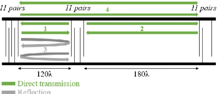
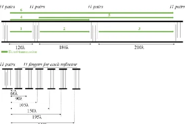
Two different configurations (with the same wavelength λ=24 µm) are compared in order to study the influence of the design on the amplitude of the peaks creating the code. The first one, conventional, has one IDT and two reflectors (see Fig. 1). The central IDT contains 11 pairs of fingers. The reflectors contain 21 fingers each. They are located at a distance of 60 λ and 90 λ from the central IDT, respectively. Both have the same aperture, equal to 1000 µm. In the second configuration, shown in Fig. 2, three IDTs (identical to those previously described) are connected together. Neither configuration has been optimized; to have similar delays in both configurations, the distances between the connected IDTs are 120 λ and 180 λ, respectively. The metallization ratio is fixed to 50% for both devices.
The COM parameters were extracted first, from harmonic admittance simulations by finite elements method (FEM). They were then used to compute the electrical response of the two configurations, using standard P-Matrix algorithms.
The devices were fabricated using an optical lithography process and a positive resist, on a lithium niobate Y128°-X cut and an LGS (0°,138.5°,26.3°) substrate. A 150 nm thin layer of aluminum (Al), gold (Au/Cr) or platinum (Pt) was deposited by RF sputtering. The process was finalized by wet etching for the aluminum layer or by ion beam etching for the gold and the platinum layers. The devices were characterized at room temperature using a probe station (Suss MicroTec PM5) and a network analyzer (VNA Agilent-N5230A). Measurements were done in the frequency domain (center frequency was fixed to the SAW device resonance and a span of 100MHz was used) and then converted to the time domain directly by the network analyzer. High temperature measurements were performed up to 600°C (the higher limit of our setup) in air, using a RF probe station (S-1160, Signatone) equipped with a high temperature probing system (S-1060, Signatone). GS Z-probes were modified in-house by adding a water-cooling element, in order to withstand high temperatures during the characterization. The evolution of the crystalline structure was analyzed by X-ray diffraction (XRD) before and after high temperature measurements.
III. RESULTS AND DISCUSSION
A. Proof of concept
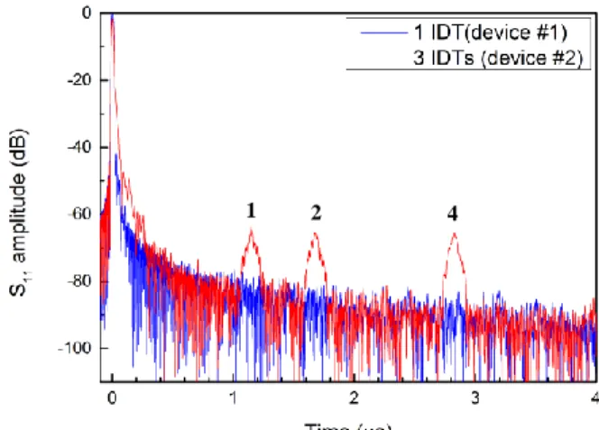
The inverse fast Fourier transform (IFFT) envelopes of the simulated S11 frequency responses for devices #1 and #2 are
presented in Fig. 3. By targeting the first two peaks, it appears that the red curve, which corresponds to the two directly transmitted signals in device #2, has a higher amplitude than the blue curve which corresponds to the two reflections in device #1. More precisely, for the design #1 (red curve), the first two peaks are due to several sequential electromechanical conversions, namely: one at the IDT for the signal emission, two at the reflectors and a last one at the IDT for the reception. In design #2 (blue curve), the first two peaks are only due to two electromechanical conversions (the first one at the IDT for
the transmission and the second one at the other IDT for the reception). So the difference around 16 dB is mostly due to the number of electromechanical conversions. The higher the number, the lower the received energy because only a part of the energy can be converted (related to the K2 value).
For device #2, some slight modification in the signal shape can be observed. This requires an additional study which is planned for future work.
The first experimental results on LN-Y128 with Al electrodes are also promising. Fig. 4 corresponds to the time domain signals and shows the same behavior as in the simulation. This good agreement between experimental and numerical results validates the model for future simulations. This also confirms the interesting features of the configuration with connected IDTs.
Fig. 3. Simulated reflection coefficient in the time domain of devices #1 and #2 on a LN-Y128 substrate with Al electrodes.
Fig. 4. Experimental reflection coefficient in the time domain of devices #1 and #2 on a LN-Y128 substrate with Al electrodes.
B. Extension to substrates with low coupling or higher losses This proof of concept made on lithium niobate can be extended to langasite in order to enable the use of ID-tags at high temperature. Fig. 5 and 6 depicts the comparison between simulations and experiments for device #1 and device #2 based on an LGS substrate with an Al metallization. Simulations show that the peaks coming from a reflection have a lower amplitude than the experimental noise level, which is around -80 dB.
Therefore, it is consistent with the fact that no signal is measured in the standard configuration with reflectors. This is mostly due to the low coupling value (K2=0.34%, [14]) and the
reflection in the LGS device. By contrast, with the three connected IDTs configuration, a signal can be identified from the noise. Each peak corresponds to a direct transmission between the IDTs.
Even if the detected amplitude is 40 dB lower than the one measured on lithium niobate, this confirms the interest of the configuration with connected IDTs on a substrate with a low K2
value. The amplitude difference is partly due to the differences in K2 values between the two substrates.
It is also interesting to see that the third peak from device #2, which corresponds to the reflection between two connected IDTs, is not detected. This confirms that the reflection is much smaller than the direct transmission.
Fig. 5. Simulated reflection coefficient in the time domain of devices #1 and #2 on an LGS substrate with Al electrodes.
Fig. 6. Experimental reflection coefficient in the time domain of devices #1 and #2 on an LGS substrate with Al electrodes.
C. High temperature measurements
According to the Literature, lithium niobate is not well suited for high temperature applications [15]. On the contrary, due to its thermal stability (up to 1000°C), LGS is currently the standard [16]. Fig. 7 and 8 show the results obtained up to 600°C with Au/Cr electrodes on LN-Y128 and LGS, respectively. After 45 minutes at 600°C, no more signal is 1 2 3 4 1 2 4 1 2 3 4 1 2 4
detectable on the LN-Y128, in contrast with the LGS substrate. The increased attenuation on LGS comes from the physical destruction of several IDT electrodes by the scratch with probe-head tips that have slipped-off due to the thermal expansion of the substrate. The images of the devices after the measurements at 600°C show that the gold electrodes are also significantly damaged by heat (see Fig. 9). Based on [17], the thin film agglomeration is related to the Tammann temperature, which is defined as:
𝑇𝑇𝑎𝑚𝑚𝑎𝑛𝑛 (°𝐾) =
𝑇𝑚𝑒𝑙𝑡𝑖𝑛𝑔 (°𝐾)
2 (1)
For gold, the value of the Tammann temperature is 395°C. It has been largely exceeded in the previous measurements, which may explain the observed phenomenon of agglomeration. Therefore, the signal loss on the LN-Y128 substrate, and its decrease on the LGS substrate after 45 minutes at 600°C, are also potentially related to the damage of gold electrodes.
Fig. 7. Experimental reflection coefficient in the time domain up to 600°C of device #2 on a LN-Y128 substrate with Au/Cr electrodes.
Fig. 8. Experimental reflection coefficient in the time domain up to 600°C of device #2 on an LGS substrate with Au/Cr electrodes.
(a) (b)
Fig. 9. Optical images of the Au/Cr electrodes (a) on a LN-Y128 substrate and (b) on an LGS substrate after measurements up to 600°C.
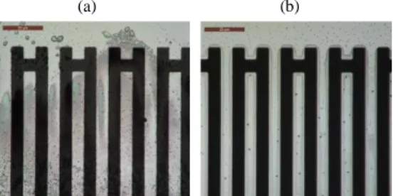
In order to remove this ambiguity, devices made with platinum electrodes were considered. Indeed, the Tammann temperature of platinum is 748°C which is high enough for the investigated temperature range. The results obtained at high temperature with the LN-Y128 and LGS substrates are given in Fig. 10 and 11, respectively. After 45 minutes at 600°C, the signals are still detectable, even for the lithium niobate substrate, which was quite unexpected. The latter shows a moderate signal attenuation with temperature, but remains operational at 600°C. The optical images of Pt electrodes on LN-Y128 and LGS at 600°C confirm that the platinum electrodes are less damaged than the gold ones (see Fig. 12).
Fig. 10. Experimental reflection coefficient in the time domain up to 600°C of device #2 on a LN-Y128 substrate with Pt electrodes.
Fig. 11. Experimental reflection coefficient in the time domain up to 600°C of device #2 on an LGS substrate with Pt electrodes.
(a) (b)
Fig. 12. Optical images of the Pt electrodes (a) on a LN-Y128 substrate and (b) on an LGS substrate after measurement up to 600°C.
In Fig. 13 and 14, a perfect superposition of the curves at room temperature before and after measurements at 600°C is observed. This clearly demonstrates that platinum has not been damaged and that both substrates (LN-Y128 and LGS) exhibit a completely reversible behavior for measurements up to 600°C. These results highlight the potential of the LN-Y128 to be used at least up to 600°C for a duration of the order of one hour. Further investigations will be conducted considering higher temperatures and longer operating times.
Moreover, the time delay (56 ns for the second peak on LN-Y128 with Pt electrodes) observed in the measurements between 25°C and 600°C looks promising for the use of the configuration with connected IDTs as a temperature sensor.
Fig. 13. Experimental reflection coefficient in the time domain at 25°C from device #2 on a LN-Y128 substrate with Pt electrodes before and after high temperature measurements.
Fig. 14. Experimental reflection coefficient in the time domain at 25°C from device #2 on an LGS substrate with Pt electrodes before and after high temperature measurements.
Fig. 15 summarizes the amplitude decrease and the time delay increase with the temperature on the devices with Au/Cr and Pt electrodes. Data was taken from the second peak, as plotted in Fig. 7 and 10. In the configuration with three connected IDTs, the first two peaks corresponding to the direct transmissions should have the same amplitude (considering that propagation losses are negligible for the LN-Y128 substrate). This is for example the case shown in Fig. 7 with Au/Cr electrodes. However, in Fig. 10 with Pt electrodes, the two peaks do not have perfectly identical amplitudes. This can be explained by a very small platinum residue that has not been etched in the 120 λ gap. Peak 1, which correspond to the propagation in the 120 λ gap, is affected by this residue. However peak 2, which is linked to a propagation in the 180 λ gap, is unaffected and was therefore used for amplitude comparisons. In Fig. 15, it is interesting to notice that the sharp amplitude decrease in the case of gold electrodes with respect to platinum is consistent with the fact that the gold electrodes were damaged.
Fig. 15. Experimental evolution of the amplitude and the time delay with temperature for device #2 made on a LN-Y128 with Au/Cr and Pt electrodes.
Fig. 16. θ-2θ XRD patterns of the LN-Y128 device #2 with Pt electrodes before and after high temperature measurements.
Finally, the XRD analysis of the LN-Y128 substrate before and after measurements at 600°C is given in Fig. 16. A new peak appears at 2θ=24.6°, which corresponds to the (004) orientation of lithium triniobate (LiNb3O8). However, the
appearance of LiNb3O8 does not seem to be detrimental for
measurements up to 600°C for 45 minutes. D. Discussion
The configuration with three connected IDTs presents a clear interest for ID-tags, but some drawbacks need to be taken into consideration. Compared with the conventional structure with reflectors (device #1), the size of the configuration with connected IDTs is larger (device #2). Moreover, there is a splitting of the RF power (of the interrogation signal) between the IDTs. This means that there is a maximum number of IDTs that can be connected together. After a given number, the signal amplitude will be lower than the one reflected in the conventional configuration, limiting the interest of the structure with connected IDTs. It could be interesting to deepen the comparison of both structures by considering an optimized design for the reflectors, as it has already been studied in [18].
Numerical simulations were done with an increased number of IDTs. In a configuration with 4 connected IDTs it is possible to generate a code thanks to the 6 peaks resulting from direct transmissions, whereas 6 reflectors are needed to obtain 6 peaks resulting from single reflections. The details of the studied devices are given in Fig. 17. For clarity, only the one-way direct transmissions have been represented.
Fig. 17. Configuration with 4 connected IDTs (device #3) and its equivalent with reflectors (device #4).
Fig. 18. Simulated reflection coefficient in the time domain of devices #3 and #4.
The simulations (see Fig. 18) show that the larger the number
of connected IDTs is, the more difficult it is to identify the direct transmission peaks. This can be explained by the fact that all electrically connected IDTs re-emit the signal when it comes to some of them. This phenomenon does not appear in the equivalent structure, even with a high number of reflectors. Moreover, the electrical interaction between connected IDTs also leads to complicated impedance matching, in contrast to the configuration with only one IDT and several reflectors. The subsequent antenna matching is an important feature to consider for remote interrogation.
In short, there is a tradeoff to be found between the amplitude level increase on one side, and the signal quality and ease of matching on the other side. With a low number of connected IDTs, the advantages of this device overcome their drawbacks in comparison to conventional designs. Thus, the concept suggested here is intended for applications that require the use of sensors with an identification functionality in harsh environments, but with a limited number of codes.
IV. CONCLUSION
A reflective delay line configuration with connected IDTs for ID-tag applications was presented and tested. The amplitude of the peaks is increased due to direct transmission, in comparison to the conventional configuration (i.e. with reflectors).
Experimental results obtained on LN-Y128 and LGS are in good agreement with simulations. This configuration with connected IDTs can further improve the performance of devices based on the well-known LN-Y128 substrate and help mitigate potential losses in harsh environments. It has also been shown that this design can be really useful for substrates where the detection of ID-tag peaks is almost impossible, like in LGS that has a poor coupling.
Electrical characterizations up to 600°C with platinum electrodes confirm the interest of the structure for operation under harsh conditions such as in high temperature environments, notably for temperature sensing. The concept can be used on LGS, which is well suited for high temperature applications, but also on LN-Y128 up to 600°C at least for 45 minutes, which was not initially expected.
Design tradeoffs regarding the signal amplitude, purity and impedance were also discussed. With the right design, this structure is very promising for wireless interrogation at long distances and at high temperature.
REFERENCES
[1] C. Floer et al., “SAW RFID devices using connected IDTs as an alternative to conventional reflectors for harsh environments,” in Proc.
2019 IEEE IFCS-EFTF, Orlando, USA, 2019, pp. 1-4.
[2] C. S. Hartmann and L. T. Claiborne, “Fundamental Limitations on Reading Range of Passive IC-Based RFID and SAW-Based RFID,” 2007
IEEE International Conference on RFID, Grapevine, TX, 2007, pp.
41-48.
[3] D. E. N. Davies, M. J. Withers and R. P. Claydon, “Passive coded transponder using an acoustic-surface-wave delay line,” in Electronics
Letters, vol. 11, no. 8, pp. 163-164, 17 April 1975.
[4] C. S. Hartmann, “Future High Volume Applications of SAW Devices,” IEEE 1985 Ultrasonics Symposium, San Francisco, CA, USA, 1985, pp. 64-73.
[5] C. Floer et al., “AlN/ZnO/LiNbO3Packageless Structure as a Low-Profile Sensor for Potential On-Body Applications,” in IEEE Transactions on
Ultrasonics, Ferroelectrics, and Frequency Control, vol. 65, no. 10, pp.
1925-1932, Oct. 2018.
[6] V. P. Plessky and L. M. Reindl, “Review on SAW RFID tags,” in IEEE
Transactions on Ultrasonics, Ferroelectrics, and Frequency Control, vol.
57, no. 3, pp. 654-668, March 2010.
[7] B. V. Sveshnikov and A. P. Shitvov, “Multitransducer SAW Device Architecture for Passive Wireless Sensor Tags,” in IEEE Transactions on
Ultrasonics, Ferroelectrics, and Frequency Control, vol. 65, no. 11, pp.
2176-2183, Nov. 2018.
[8] C. K. Campbell, “Surface Acoustic Wave Devices for Mobile and Wireless Communications,” San Diego, CA, USA: Academic, 1998.
[9] T. Aubert et al., “Investigations on AlN/sapphire piezoelectric bilayer structure for high-temperature SAW applications,” in IEEE Transactions
on Ultrasonics, Ferroelectrics, and Frequency Control, vol. 59, no. 5, pp.
999-1005, May 2012.
[10] R.C. Turner, P.A. Fuierer, R.E. Newnham and T.R. Shrout, “Materials for high temperature acoustic and vibration sensors: A review,” Applied
Acoustics, vol. 41, no. 4, pp. 299-324,1994.
[11] A. Binder, G. Bruckner, and J. Bardong, “Passive SAW Based RFID Systems Finding their Way to Harsh Environment Applications,” 2013
Proceedings of the SENSORCOMM, pp. 57-62.
[12] T. Vandahl, M. Rusko, F. Moller and W. Buff, “New SAW sensor-device with identification capability,” 1995 IEEE Ultrasonics Symposium.
Proceedings. An International Symposium, Seattle, WA, USA, 1995, pp.
535-538 vol.1.
[13] W. Buff, M. Goroll, S. Klett, M. Rusko, M. Binhack and J. Ehrenpfordt, “Wireless Passive Remote Sensing with Saw Resonators and a New Solution for Identification Problems in Multiple Sensor Systems,” 1999
29th European Microwave Conference, Munich, Germany, 1999, pp.
391-394.
[14] N. Naumenko and L. Solie, “Optimal cuts of langasite, La3Ga5SiO14 for
SAW devices,” in IEEE Transactions on Ultrasonics, Ferroelectrics, and
Frequency Control, vol. 48, no. 2, pp. 530-537, March 2001.
[15] R. Hauser, L. Reindl and J. Biniasch, “High-temperature stability of LiNbO3 based SAW devices,” IEEE Symposium on Ultrasonics, 2003,
Honolulu, HI, USA, 2003, pp. 192-195 vol.1.
[16] T. Aubert and O. Elmazria, “Stability of langasite regarding SAW applications above 800°C in air atmosphere,” 2012 IEEE International
Ultrasonics Symposium, Dresden, 2012, pp. 2098-2101.
[17] T. Aubert, “Contribution à l'élaboration de capteurs sans-fil, opérant à très haute température (500-1000ºC), à base de dispositifs à ondes élastiques de surface: choix des matériaux constitutifs,” Ph.D. dissertation, Henri-Poincaré Univ., Nancy, 2010.
[18] K. Yamanouchi, G. Shimizu and K. Morishita, "2.5 GHz-range SAW propagation and reflection characteristics and application to passive electronic tag and matched filter," 1993 Proceedings IEEE Ultrasonics
Symposium, Baltimore, MD, USA, 1993, pp. 1267-1270 vol.2.
Cécile Floer (M’2016) was born in Sarreguemines, France, in 1993. She
graduated from a leading national
engineering school specializing in
mechanical and electrical engineering (ENSEM, Nancy, France) in 2016.
She joined the Micro-nanosystems group of the Institut Jean Lamour, (Université de Lorraine-CNRS), as a Ph.D. candidate. Her research interest is the development of SAW devices for biomedical applications. Ms. Floer serves as a student representative at the IEEE Adcom committee from 2018 to 2020.
Sami Hage-Ali was born in Strasbourg,
France, in 1982. He received an
Engineering Degree from Ecole Centrale
de Lille and a M.S in
micro-nanotechnology from University of Lille 1 in 2005. He received another Master degree in international projects engineering from University of Lille 1 in 2006. He received a
Ph.D. in micro-nanotechnology, acoustics and
telecommunications in 2011. In 2011, Dr Hage-Ali was awarded a Fulbright grant and became a post-doctoral fellow at University of Illinois at Urbana-Champaign, USA.
Since 2014, he is an associate professor at University of Lorraine and is with the Micro-nanosystems group of Institut Jean Lamour, Nancy, France. Dr Hage-Ali’s areas of research are flexible/stretchable electronics, micro-nanosystems, microwaves, antennas and surface acoustic wave sensors.
He is currently serving as chairman of the IEEE France Section Sensors Council Chapter.
Pascal Nicolay was born in Metz, France, in 1977. He received an Engineering Diploma in 2001 from the Ecole Nationale Supérieure
en Génie des Systèmes Industriels
(ENSGSI), Nancy, France. He then received his M.Sc. (2004) and Ph.D. (2007) in applied physics from the University of Lorraine. In 2018, he received his Habilitation from the University of Technology of Compiègne. Pascal worked four years (2001-2004) as a Chargé d’Affaires for the French Innovation Agency (OSEO). He then worked three years (2008-2011) for TDK-EPCOS and eight years (2011-2019) for CTR (Carinthian Tech Research AG), as an R&D Project Manager in the field of SAW RF Filters and SAW Wireless Sensors.
In 2019, he joined the Carinthia University of Applied Science, and is now director of the Carinthia Institute for Smart Materials and Manufacturing Technologies (CiSMAT). He currently holds a KWF-endowed Professorship for Smart Materials.
Hugo Chambon was born in Montpellier, France, in 1991. He received his mechanical engineering degrees from ENSMM in Besançon and Supméca in Paris in 2015.
He is currently pursuing his Ph.D. at CTR (Carinthian Tech Research), in partnership with the University of Technology of Compiègne. His research interests include surface acoustic wave sensors and filters.
Sergei Zhgoon (A’96–M’96–SM’09)
graduated from Moscow Power
Engineering Institute (MPEI) in 1974
(present name: National Research
University MPEI). He received his Ph.D. degree from the same university in 1979. In 1986, he was awarded the degree of Senior Research Fellow.
Since 1974 he has been permanently working at the Department of Radio Engineering Fundamentals in MPEI. Since 1983 he has been the head of the laboratory in this department. His present research interests are in surface acoustic wave (SAW) devices since 1975. His main areas of expertise presently include all aspects of microwave acoustics device fundamentals, design of SAW/BAW filters, resonators, RF ID tags and their preparation techniques, thin film deposition and patterning, advanced chip-scale and wafer-scale packaging with MEMS-like techniques, surface acoustic wave propagation in multilayered and strained media, and SAW sensors based on these phenomena.
Dr. Zhgoon has co-authored over 210 publications and about 20 patents. He has supervised over 20 M.S. and 4 Ph.D. students in MPEI.
Alexander Shvetsov was born in the Moscow region, Russia, in 1979. He has been working in the SAW devices research group at the Moscow Power Engineering Institute (contemporary name: National Research University MPEI) from 2001. He received a B.S. degree in 2004 and a M.S. degree in 2011 from MPEI in radio engineering. He received his Ph.D. degree in radio engineering from Moscow Technical University of Communications and Informatics in 2017.
His scientific interests currently involve effects of acoustic wave propagation and properties of piezoelectric transducers applied to signal processing devices and sensors. His work is reflected in more than 40 technical papers published from 2003 to 2019.
Jérémy Streque received the Ingénieur degree from École Centrale de Lille, France, and the M.S. degree from the Lille University of Science and Technology in 2007. He then received the Ph.D. degree from École Centrale de Lille in 2011, with a focus on magnetostatic actuation and soft materials for MEMS. He carried out his Ph.D. research at Institute of Electronics, Micro-electronics, and Nanotechnology. In 2012, he joined GeorgiaTech-CNRS, Metz, France, a Joint Laboratory focused on III-Nitrides for solar cells and sensors, and then worked for the launch of Institut Lafayette, Metz, a scientific private platform dedicated to these topics.
He is currently a researcher at Institut Jean Lamour, Nancy, France. His current areas of research are piezoelectric materials and SAW sensors for high temperature applications.
Hamid M’Jahed received his Master degree in electronics and industrial automation in 1993. He joined the Institut Jean Lamour as permanent CNRS (National Center for Scientific Research) staff.
Now he is CNRS engineer in RF and Electronics. His main research interests include study and realization of system query for SAW wireless sensors. In 2011, he receives the Crystal award as the best Engineer in CNRS.
Omar Elmazria (M’2001–SM’16)
received his Ph.D. degree in electronics from Metz University, France, in 1996 and he joined the University of Nancy I as associate Professor of electronic and communication systems in 1997 and as a full Professor in 2003.
He was the Head of the Micro-nanosystems group within the Institut Jean Lamour. His current research focus on layered structures-based surface acoustic waves (SAW) devices for communication systems and sensing applications.
Pr. Elmazria co-authored more than 150 papers in refereed international journals and in proceeding of international conferences. In 2017, he received the medal of URSI-France (International Union of Radio Science).