Publisher’s version / Version de l'éditeur:
Applied Physics Letters, 86, 25, pp. 252507-1-252507-3, 2005-05-16
READ THESE TERMS AND CONDITIONS CAREFULLY BEFORE USING THIS WEBSITE. https://nrc-publications.canada.ca/eng/copyright
Vous avez des questions? Nous pouvons vous aider. Pour communiquer directement avec un auteur, consultez la première page de la revue dans laquelle son article a été publié afin de trouver ses coordonnées. Si vous n’arrivez pas à les repérer, communiquez avec nous à PublicationsArchive-ArchivesPublications@nrc-cnrc.gc.ca.
Questions? Contact the NRC Publications Archive team at
PublicationsArchive-ArchivesPublications@nrc-cnrc.gc.ca. If you wish to email the authors directly, please see the first page of the publication for their contact information.
NRC Publications Archive
Archives des publications du CNRC
This publication could be one of several versions: author’s original, accepted manuscript or the publisher’s version. / La version de cette publication peut être l’une des suivantes : la version prépublication de l’auteur, la version acceptée du manuscrit ou la version de l’éditeur.
For the publisher’s version, please access the DOI link below./ Pour consulter la version de l’éditeur, utilisez le lien DOI ci-dessous.
https://doi.org/10.1063/1.1952572
Access and use of this website and the material on it are subject to the Terms and Conditions set forth at
Effect of Antiphase Boundaries on Electrical Transport Properties of
Fe3O4 Nanostructures
Li, Hongliang; Wu, Yihong; Guo, Zaibing; Wang, Shijie; Teo, Kie Leong;
Veres, Teodor
https://publications-cnrc.canada.ca/fra/droits
L’accès à ce site Web et l’utilisation de son contenu sont assujettis aux conditions présentées dans le site LISEZ CES CONDITIONS ATTENTIVEMENT AVANT D’UTILISER CE SITE WEB.
NRC Publications Record / Notice d'Archives des publications de CNRC:
https://nrc-publications.canada.ca/eng/view/object/?id=959359a6-1943-4e99-9915-944a707a47d3 https://publications-cnrc.canada.ca/fra/voir/objet/?id=959359a6-1943-4e99-9915-944a707a47d3Effect of antiphase boundaries on electrical transport properties of Fe
3O
4nanostructures
Hongliang Li and Yihong Wua!
Department of Electrical and Computer Engineering, National University of Singapore, 4 Engineering Drive 3, Singapore 117576 and Data Storage Institute, DSI Building, 5 Engineering Drive 1, Singapore 117608
Zaibing Guo
Data Storage Institute, DSI Building, 5 Engineering Drive 1, Singapore 117608
Shijie Wang
Institute of Materials Research and Engineering (IMRE), 3 Research Link, Singapore 117602
Kie Leong Teo
Department of Electrical and Computer Engineering, National University of Singapore, 4 Engineering Drive 3, Singapore 117576
Teodor Veres
Industrial Materials Institute, National Research Council Canada, 75, de Mortagne, Boucherville, Québec, Canada, J4B 6Y4
sReceived 3 February 2005; accepted 16 May 2005; published online 15 June 2005d
Fe3O4 nanowires have been fabricated based on Fe3O4 thin films grown on a-Al2O3 s0001d substrates using the hard mask and ion milling technique. Compared with thin films, the Fe3O4 nanowire exhibits a slightly sharper Verwey transition but pronounced anisotropic magnetoresistance properties in the film plane at low magnetic field. Detailed bias-dependence study of both the conductance and magnetoresistance curves for both the thin films and nanowires suggests that the electrical conduction in magnetite near and above the Verwey transition temperature is dominated by a tunneling mechanism across antiphase boundaries. © 2005 American
Institute of Physics. fDOI: 10.1063/1.1952572g
Recently, half-metals have received increasing attention because of its potential applications in spintronic devices.1,2 Among several different types of half-metallic materials, magnetite sFe3O4dhas been studied most intensively because of its highest known Curie temperature s858 Kd and simplest chemical and crystalline structure, which allows for easy in-tegration with existing metal-based giant magnetoresistance devices. Antiphase boundaries sAPBsd, as a kind of growth defect in Fe3O4thin films, were reported in the literature by different groups with different substrates and growth techniques.3–5It is commonly believed that APBs are intrsic consequences of nucleation and a growth mechanism in-dependent of preparation methods and substrates. From a practical application point of view, it is of great importance to obtain an understanding of how the APBs affect the elec-trical transport properties of the magnetite. Eerenstein et al. showed that epitaxial film with APBs has linear I/V curves and interpreted the transport properties across APBs in term of small polaron hopping.6 As the effect of APBs on the electron transport properties of thin films is very much de-pendent on the density of the APBs, it necessitates more detailed investigations through confining the APBs into a one-dimensional conduction channel. In this letter, we report a systematic study of the transport properties of both epitax-ial Fe3O4 thin films and nanowires. The latter allow us to confine the APBs in a nanowire, which makes the effect of APBs more prominent as compared to the thin-film case, as
conduction paths through the host material are relatively re-duced. The bias dependence of conductance and magnetore-sistance sMRd suggests that the electron transport of Fe3O4 nanowires is well represented by a series of tunnel junctions made by APBs.
The Fe3O4thin films saround 150 nmd were prepared on
a-Al2O3 s0001d single-crystal substrates using molecular-beam epitaxy with a background pressure of about 10−9 Torr. During the growth, iron metal was evaporated by an electron beam with an oxygen partial pressure of 1.0310−5 Torr. The deposition rate was about 0.04 nm/s at a substrate tempera-ture of 573 K. The structural, magnetic, and transport prop-erties of the as-grown thin films were characterized by tran-sition electron microscopy sTEMd, superconducting quantum interference device magnetometer, and dc four-probe tech-niques, respectively. The nanowires were fabricated using electroplated Ni nanowires saverage diameter of 200 nm and a length of 30mmd as the hard mask. The typical fabrication processes involve dispersing the Ni nanowires on the as-grown Fe3O4 thin film, ion milling of uncovered film, re-moval of the Ni nanowires by ultrasonic cleaning, and elec-trode formation using a double-layer resist process. The location of nanowires, and the positioning and deposition of electrodes fTis20 nmd/Aus100 nmdg were performed with a laser writer and an e-beam evaporator, respectively. The fi-nally finished Fe3O4nanowire has a width of about 300 nm. A dark-field TEM plane-view micrograph is shown in Fig. 1sad. The black lines are antiphase boundaries, which are irregular with an average size of ,100 nm. No other defects were found except the APBs, which is consistent with the
adAuthor to whom correspondence should be addressed; electronic mail:
elewuyh@nus.edu.sg
APPLIED PHYSICS LETTERS 86, 252507 s2005d
0003-6951/2005/86~25!/252507/3/$22.50 86, 252507-1 © 2005 American Institute of Physics
x-ray diffraction result snot shown hered. Compared to the domain size of the sample by Moussy et al.,5 our sample shows a larger average domain size due to the thicker film. In Fig. 1sbd, we can observe more clearly APBs by magnifying one of them along the arrow direction.
Figure 2sad shows the temperature dependence of the resistance RsTd normalized to the room temperature resis-tance R s300 Kd for both a thin film and a nanowire. The resistivity of our film is ,0.008 V cm, which is slightly higher than the bulk value of 0.005 V cm, and much less than 0.18 V cm in the polycrystalline sample reported.7 A clear Verwey transition is seen in both curves at 120 K in the temperature-dependent resistance curve. Although it is not so obvious, the nanowire indeed shows a slightly sharper tran-sition compared to the thin film, which is expected due to the decrease in randomness inside a smaller volume of sample. The magnetization versus temperature of zero-field-cooled sMZFCd and field-cooled sMFCd thin film with 100 Oe field applied are shown in the inset of Fig. 2sad. We can clearly see a sharp decrease in the magnetic moment around 120 K. Both of them are strong indicators of good stoichiometry and high crystalline phase of the thin film.8
Figure 2sbd shows the typical magnetoresistance curves at 300 K. The in-plane MR is isotropic for thin films, but it is
anisotropic for the nanowires. The MR ratio of thin film is about 1% at a magnetic field of 6000 Oe. The nanowire ex-hibits an almost the same MR as that of the thin film in the longitudinal direction, but a somewhat reduced MR in the transverse direction. The former shows a shape that is uni-versal to almost all the Fe3O4 films grown by different techniques.6,7,9,10 We believe that the exchange coupling across APBs should be antiferromagnetic, as discussed in Refs. 6 and 9. Depending on the domain size, the spins at the center of the domains may switch earlier or easier than those at the boundaries. This may explain the difference in the MR curves at low and high fields. This argument is also sup-ported by the slow change of transverse MR of nanowires at low field which can be understood as caused by the shape anisotropy in the center region of the domain, whereas in the high-field region the MR curve is almost the same as that in the longitudinal direction. The inset of Fig. 2sbd shows the thin film MR curve at a high magnetic field. It can be seen that the MR curve is unsaturated even at an applied field of 7 T, which is consistent with most observations that the Fe3O4 magnetization is difficult to saturate due to the exis-tence of atomically sharp antiphase boundaries. It is interest-ing to note that the large MR at high fields does not corre-spond to a large change of magnetization in the same field range. In other words, the MR at high field is caused mainly by the spin alignment at the boundaries instead of the center region of the domains. As it will be discussed subsequently, the transport across the APBs is dominated by tunneling.
The typical differential conductance-voltage curve for a nanowire is shown in Fig. 3, which was measured at a tem-perature of 130 K. The curves at other temtem-peratures ranging from 110 to 300 K exhibit almost the same parabolic shape except for the absolute values, which are dependent on tem-perature. As shown in Fig. 3, the conductance-voltage curve can be fitted almost perfectly to a parabola using GsVd =aV2+bV+G0, where aandb are constants and G0 is the zero-bias conductance. Although it is not shown here, a simi-lar degree of agreement between experimental and fitted curves has also been obtained for the conductance curves at all other temperatures which we have investigated.bis neg-ligibly small compared toa in the entire temperature range, suggesting that the transport is dominated by tunneling across APBs. Also shown in the figure is the conductance curve taken at an applied field of 5 T. If we assume a rect-angular shape of potential barrier with a height of f and
thickness d, then according to the Simmons model,11one has
G0~1/d anda~ d/f. The increase of zero-bias conductance
FIG. 1. sad Plane-view TEM images of Fe3O4thin film. The black lines are
antiphase boundaries. sbd Magnified APB as indicated by the arrow.
FIG. 2. sad Resistance as a function of temperature for both a thin film and a nanowire; Inset: ZFC and FC curves of the thin film with a magnetic field of 100 Oe. sbd Normalized MR curve for both thin films and nanowires at 300 K snanowireIP: field parallel to the wire axis; nanowireIV: field perpen-dicular to the wire axisd. Inset: high-field MR of the thin film at 300 K.
FIG. 3. Bias dependence of differential conductance for a nanowire at 130 K with applied magnetic fields of 0 and 5 T, respectively. Solid curve: fitted data according to the Simmons equation; solid circles: experimental data at zero field; open circles: experimental data at 5 T. Inset: bias depen-dence of G8.
252507-2 Liet al. Appl. Phys. Lett. 86, 252507 ~2005!
with an external field may be attributed to a decrease of barrier thickness. Shown in the inset of Fig. 3sad is the bias voltage dependence of GsVd
8
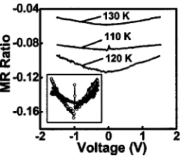
=fGsH=0,Vd/GsH=0,0dg/ fGsH=5 T,Vd/GsH=5 T,0g. Substituting G0~1/d and a~ d/f into the equation, one finds d2sHd/fsHd , d2s0d/fs0d. As the potential barrier will either not change or will decrease with external field, it implies again that the barrier thickness decreases with the external field.It is well known from the work on magnetic tunnel junc-tions that the MR ratio normally decreases with the bias volt-age. Figure 4 shows the bias dependence of MR ratio DR/R0=sRs5 Td−R0d/R0at 110, 120, and 130 K for the nano-wire sample. It was obtained by first measuring the I-V curve at zero field and then repeating the measurement at an ap-plied field of 5 T. The MR shows a minimum value at 120 K which is consistent with other groups’ results.12–14 The MR ratio increases with increasing the bias, which is a typical behavior of magnetic tunneling junctions. The thin film also shows the same bias dependence of MR, although it is not as obvious as the nanowire case ssee the inset of Fig. 4d. As it is
shown in the inset, we also observe a zero-bias MR anomaly at 110 K for the nanowire sample that is not well understood at present.
In summary, our systematic study of the transport prop-erties of Fe3O4thin films and nanowires suggests that APBs have a strong effect on electrical transport properties in Fe3O4. Antiferromagnetic coupling across the APBs is re-sponsible for the universal shape of the MR curves and the transport across the APBs is dominated by tunneling.
1S. A. Wolf, D. D. Awschalom, R. A. Buhrman, J. M. Daughton, S. von
Molnár, M. L. Roukes, A. Y. Chtchelkanova, and D. M. Treger, Science
294, 1488 s2001d.
2I. Žutić, J. Fabian, and S. Das Sarma, Rev. Mod. Phys. 76, 323 s2004d. 3D. T. Margulies, F. T. Parker, M. L. Rudee, F. E. Spada, J. N. Chapman, P.
R. Aitchison, and A. E. Berkowitz, Phys. Rev. Lett. 79, 5162 s1997d.
4W. L. Zhou, K.-Y. Wang, C. J. O’Connor, and J. Tang, J. Appl. Phys. 89,
7398 s2001d.
5J.-B. Moussy, S. Gota, A. Bataille, M.-J. Guittet, M. Gautier-Soyer, F.
Delille, B. Dieny, F. Ott, T. D. Doan, P. Warin, P. Bayle-Guillemaud, C. Gatel, and E. Snoeck, Phys. Rev. B 70, 174448 s2004d.
6W. Eerenstein, T. T. M. Palstra, S. S. Saxena, and T. Hibma, Phys. Rev.
Lett. 88, 247204 s2002d.
7Hui Liu, E. Y. Jiang, H. L. Bai, R. K. Zheng, H. L. Wei, and X. X. Zhang,
Appl. Phys. Lett. 83, 3531 s2003d.
8E. Lochner, K. A. Shaw, R. C. Dibari, W. Portwine, P. Stoyonov, S. D.
Berry, and D. M. Lind, IEEE Trans. Magn. 30, 4912 s1994d.
9M. Ziese and H. J. Blythe, J. Phys.: Condens. Matter 12, 13 s2000d. 10M. Ziese, R. Höhne, H. C. Semmelhack, H. Reckentin, N. H. Hong, and P.
Esquinazi, Eur. Phys. J. B 28, 415 s2002d.
11J. G. Simmons, J. Appl. Phys. 34, 1793 s1963d.
12S. B. Ogale, K. Ghosh, R. P. Sharma, R. L. Greene, R. Ramesh, and T.
Venkatesan, Phys. Rev. B 57, 7823 s1998d.
13X. W. Li, A. Gupta, G. Xiao, and G. Q. Gong, J. Appl. Phys. 83, 7049
s1998d.
14G. Q. Gong, A. Gupta, G. Xiao, W. Qian, and V. P. Dravid, Phys. Rev. B 56, 5096 s1997d.
FIG. 4. Bias dependence of MR for the nanowire at 110, 120, and 130 K. Inset: comparison of bias dependence of MR for the thin film ssolid circlesd and nanowire sopen circlesd at 110 K.
252507-3 Liet al. Appl. Phys. Lett. 86, 252507 ~2005!