HAL Id: hal-01575130
https://hal.archives-ouvertes.fr/hal-01575130
Submitted on 17 Aug 2017
HAL is a multi-disciplinary open access
archive for the deposit and dissemination of
sci-entific research documents, whether they are
pub-lished or not. The documents may come from
teaching and research institutions in France or
abroad, or from public or private research centers.
L’archive ouverte pluridisciplinaire HAL, est
destinée au dépôt et à la diffusion de documents
scientifiques de niveau recherche, publiés ou non,
émanant des établissements d’enseignement et de
recherche français ou étrangers, des laboratoires
publics ou privés.
Mechanisms of power module source metal degradation
during electro-thermal aging
Roberta Ruffilli, Mounira Berkani, Philippe Dupuy, Stéphane Lefebvre, Yann
Weber, Marc Legros
To cite this version:
Roberta Ruffilli, Mounira Berkani, Philippe Dupuy, Stéphane Lefebvre, Yann Weber, et al..
Mech-anisms of power module source metal degradation during electro-thermal aging. Microelectronics
Reliability, Elsevier, 2017, 76-77, pp.507 - 511. �10.1016/j.microrel.2017.06.086�. �hal-01575130�
Mechanisms of power module source metal degradation during
electro-thermal aging.
R. Ruffilli
a,c*
, M. Berkani
b, P. Dupuy
c,S. Lefebvre
b, Y. Weber
c, M. Legros
aaCEMES-CNRS, 29 rue J. Marvig, Université de Toulouse, 31055 Toulouse, France
bLaboratoire SATIE, ENS-Cachan, 61 Avenue du Président Wilson, 94235 Cachan, France
cNXP Semiconductors France SAS, 134 Avenue du Général Eisenhower, 31100 Toulouse, France
Abstract
The long-term reliability of power devices for applications in the automotive industry is limited by the electro-thermal and/or thermo-mechanical aging of the metallic parts. In the present work, we characterize the bonding wire and source metallization degradation of power MOSFETs-based devices under accelerated aging conditions, through electron and ion microscopy. The metal degradation is driven by an enhanced self-diffusion of aluminium (Al) atoms along the grain boundaries and a generalized fatigue crack propagation from the surface down to the silicon (Si) bulk. The metallization under the wire bonds is a critical location because it is initially plastically deformed during the bonding process. In addition, the wire-metal interface presents several imperfections, such as small cavities and Al oxide residues. During the electro-thermal cycles, they could be the starting point for harmful cracks that run along the interface (and eventually cause the wire lift-off or the cracking of the substrate). Whichever the propagation direction, the generation of these cracks locally increases the device resistance and temperature, and accelerates the aging process until failure.
Mechanisms of power module source metal degradation during
electro-thermal aging.
R. Ruffilli
a,c*
, M. Berkani
b, P. Dupuy
c,S. Lefebvre
b, Y. Weber
c, M. Legros
a1. Introduction
In the reliability chain of power modules, the metallization and wire bondings constitute a key link as they are more prone to plastic deformation [1–3]. The main sources of mechanical stress arise from the differential between the coefficient of thermal expansion (CTE) between the metal and the oxide/semiconducting parts. As aging progresses, the degradation of the metal may increase its resistance, which in turn will increase the temperature of the device in the on-state and therefore augment the mechanical stress. This feedback causes a degradation of the top metal through specific processes [4,5]. The wire bondings, that are ultrasonic cold welded on top of this metallization, complexify significantly the initial device structure [6]. In the present work, we report how we can access the structure of both the metallization and the bonded wire but also their interface even in its damaged state. New observations indicate that catastrophic failure of the device initiate in this aged interfacial region before propagating into the substrate. This mode of degradation of Al and Al bonding wires is widely encountered in power MOSFETs aging and may be of interest for manufacturers and users.
2. Experimental procedure
2.1. Device under test and accelerated aging tests
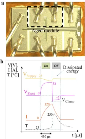
The device under test is a 12 V SmartMOS module from NXP Semiconductors designed for car applications. The power die (Fig. 1) consists in five MOS sectors, connected by eight Al wedge bond wires having a diameter of 380 µm (15 mils). Here we focus on the interface between the wires and the Al (0.5 wt% Cu and W) source metallization, which is 3.6 µm thick.
We performed specific aging tests (AECQ100-12 [7]) at 70°C, putting the device under repetitive short-circuit conditions until failure [5,8]. During the tests,
only one sector undergoes the electrical pulses (by using an external gate driver and suppressing the control die functionalities), so the others can serve as reference for the microstructural characterization of the metallic part. The life time of DUT spans between 300k and 5Mcycles depending on the test temperature [6].
Fig. 1. (a) Power die of a 12 V SmartMOS from NXP Semiconductors showing 5 sectors. Only the central-lower one is electro-thermally aged. (b) Typical signals during a short-circuit event in the power device by activation of overload protection. Temperature has been simulated using
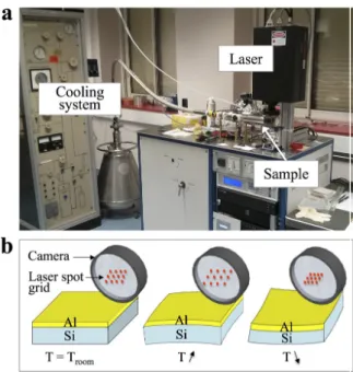
Fig. 2. (a) Thermal aging test bench. (b) Schematic illustration of the laser spot behavior depending on the
Si-Al wafer curvature during the thermal cycles.
Fig. 3. SEM images of the source metal surface of a (a) non-aged module and an (b) aged one and relative cross-sections of a (c) non-aged module and an (d) aged one.
Scale bar 2.5 µm.
2.2. Thermal cycles – curvature experiment
In parallel, thermal-only cycles (from - 190 °C to + 350 °C) were performed under vacuum in a home-made test bench (Fig. 2a) based on a KSA MOS laser reflectometer and an ARS cryo-holder. The tested samples are reference power dies (without the bonding wire connections). During the tests, the curvature imposed by the Al film to the Si substrate (due to the difference in CTE) is measured by laser profilometry (Fig. 2b). The Stoney equation [9,10] is used to obtain
directly the stress variations in the Al film. These thermal tests were not performed in sufficient numbers to induce significant aging of the device. In the following, aged devices only refer to those that have endured repetitive short-circuits, corresponding to electro-thermal cycles.
2.3. Microstructural characterization
Preliminary surface (Fig. 3a,b) and cross-sectional (Fig. 3c,d) observations of the source metallization were performed in a Helios 600 FIB/SEM (Focused Ion Beam/Scanning Electron Microscope) from FEI before and after electro-thermal cycles, confirming a heavy surface reconstruction upon aging.
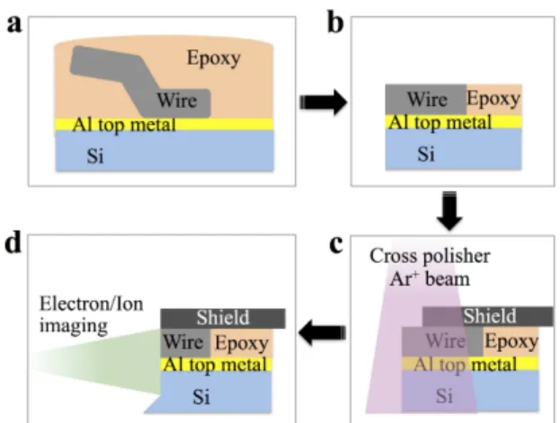
To increase the observation areas and to disclose the whole wire-metallization interface without damaging their microstructure, the device was then prepared using an ion beam Cross-Polisher (CP) from JEOL. In the CP, a 6 kV argon ion (Ar+) beam irradiates the region of interest and creates a mirrored face for FIB/SEM inspection (Fig. 4d). The whole process, explained through Fig. 4, consists in covering the power die with conductive epoxy (G-1, Gatan Inc. mixed with Carbon Paint from Agar Scientific) (Fig. 4a), curing it overnight at ~80°C, mechanically polishing it parallel to the metallization (Fig. 4b) before applying a mask across the selected area and milling it at 90° from the top surface (Fig. 4c).
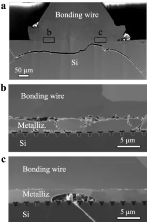
As-processed and aged devices were observed in the FIB/SEM using electron and ion channelling contrast, the latter being strictly dependent on the grain orientation [11]. Fig. 5a shows a low magnification SEM image of the bonding wire from a non-aged module.
At higher magnification (Fig. 5b), the ion image of the wire-metal interface reveals a strong plastic and uneven deformation imposed by the bonding process to the Al metallization prior to aging As will be explained later, his plastic deformation locally induces a smaller grain size and wavy interfaces.
Finally, Energy Dispersive X-Ray (EDX) analysis in the FIB/SEM has been used to analyze the severe cracking occurring at failure in the region beneath the bonding wire.
Fig. 4. Illustration of cross-sectional preparation of the wire-Al top metal interface: 1) embedding in epoxy resin,
2) mechanical polishing of the top surface parallel to the bulk, 3) 90° mechanical polishing, 4) imaging.
Fig. 5. (a) SEM cross-sectional imaging of the bonding wire from a non-aged power module and (b) higher magnification ionic image of the wire-metallization
interface.
3. Results
3.1. Al metallization outside of the bonding area
Away from the bonding contacts, the initial metallization structure (Fig. 3a,c) is characterized by a grain size on the same order of the metallization thickness, with most of the grain boundaries (GBs) perpendicular to the surface (bamboo structure).
We know that the repetitive electro-thermal cycles induce plastic deformation and surface reconstruction
in the Al metal (Fig. 3b,d). Typically, successive short-circuits of several tens of microseconds induce temperature gradients on the order of 200°C [12].
To try to better quantify this plastic deformation, we have performed pure thermal cycles with various amplitudes on a naked die (equivalent to a 4 micron thin Al film deposited on a 260 micron thick Si substrate) using our custom reflectometer. On this set-up, the temperature gradients (20°C/min) cannot be as steep as those in electrically induced short-circuits, but the temperature amplitude (between the lower and upper temperature) can be significantly increased. The amount of strain per cycle is therefore larger. This method has been widely employed to figure out the mechanisms at play during the deformation of metallic films on rigid substrates [13–15]. Fig. 6 shows one of these cycles between -190° and 350°C. The larger CTE of the Al film compared to the Si substrate induces elastic and plastic strains in the film. Starting the experiment at -190°C, the metallic layer yields in compression (c) during heating, before being stressed in tension (t) upon cooling. As expected, the elastic regime is shorter at high temperature than at low temperature. Between these elastic parts in tension and compression, most of the stress relaxes by plastic deformation. The dominant role of diffusion in the relaxation is evidenced by the much lower stress levels reached at high temperature. In a former study, we supposed that the role of dislocation-based relaxation may be significant only during the first temperature excursions. Moving pre-existing dislocations inside single initially large bamboo grains causes the formation of subgrains (grains with a misorientation lower than 10°) [6].
Fig. 6. Stress-Temperature cycle for the Al thin film deposited onto the Si wafer. The relative stress is measured
along the larger die dimension, and the zero value is here taken at 350°C. The cycle is initiated at T=-190°C, and the
Then GB diffusive deformation largely dominates plastic strain due to thermal gradients [4,5]. In electro-thermally aged devices, diffusion, and especially GB diffusion, is very probably at the origin of cavities formation as well as cracks running from the surface to the transistor area following the GBs (Fig. 3d).
The temperature amplitude of the thermal cycles performed in the reflectometer is larger than the temperature gradients occurring during electro-thermal aging. This certainly increases the plastic strain per cycle (including GB diffusive deformation), but only a few cycles can be reached with this method, much fewer than the hundreds of thousands (or millions) that the power dies undergo under short-circuit conditions. The temperature gradients imposed are also much smoother.
After about 5 cycles, no surface change (cracks, slip traces) has been observed using SEM/FIB and EBSD (Electron Back-Scattered Diffraction) mapping. In the following, the structural changes in the metallization and wire are the consequence of accelerated electro-thermal aging tests (successive short-circuits).
3.2. Wire-metallization interface
Under the wire, the initial Al metallization (Fig. 5) has endured plastic deformation due to the bonding process. The grain size is systematically smaller in these zones, compared to the bamboo structure of the naked metallization. On the other side, the grains in the Al wire are much larger. In a previous work [6], we show that this deformation ranges from 2% to 27% and is highly uneven. Moreover, the bonding between the metallization and the wire is imperfect and contains, voids and residues of native oxide.
Upon aging (Fig. 7), the amount of plastic deformation perpendicular to the interface does not change significantly but severe fatigue crack phenomena are observed within the metallization (Fig. 7b). Cracks run parallel to the surface, along the bonding imperfections, causing an electrical contact reduction between the wire and the metallization. At the same time, additional cracks run from the surface to the MOSFET area following the grain boundaries.
At this point, cracks may appear also in the Si substrate (Figs. 7a,c and 8a,b) under the bonding area, where current densities are maximum. They are probably caused by an abrupt short-circuit event. Here, we have observed two different crack types: 1) a thicker one, visible at lower magnification in Fig. 7a, and 2) a finer one, showed at higher magnification in Figs. 7c and 8a,b. The latter are connected to cavities
Fig. 7. (a) SEM cross-sectional imaging of the bonding wire from an aged power module showing different types of cracks, (b), (c) ionic higher magnification images of the wire- metallization interface located in the boxes (b) and (c) in a).
The die crack resulted from an electro-thermal
event occurring at failure time.
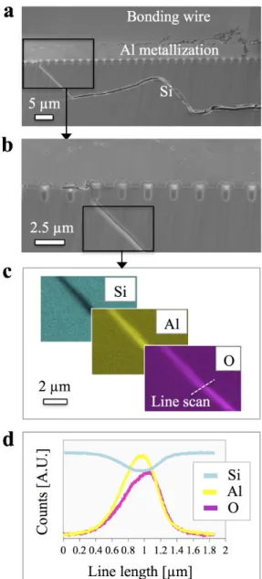
in the Al metallization (Fig. 7c) that are larger and rounder than the fatigue cracks generated by electro-thermal aging (Figs. 7b and 3d). Moreover, these metallization-bound cracks are filled with Al, as shown in the EDX maps of a crack portion (Fig. 8c) and in the relative live scan plot (Fig. 8d), representing the element distribution along the dashed line in Fig. 8c. This suggests that local melting or large Al diffusion took place in a device that remained hot long enough, or that kept conducting a current despite not functioning anymore (these damages are too important and have obviously destroyed several transistors). On the other side, the larger cracks in the Si bulk are not filled with Al, meaning that the device was completely failed, non-conductive and cold.
We can therefore suppose that the device kept conducting current for some time after the apparition
Fig. 8. (a) Low and (b) high magnification SEM image of the cracked Si bulk under the bonding contact. (c) EDX mapping of the crack in the Si bulk and (d) relative line scan plot showing the element distribution along the
dashed line in (c).
of the first cracks connected to the metallization (those filled with Al).
The larger cracks that span over the whole area under the wire bonding (Fig. 7a) caused the final failure of the device, which ceased to operate and cooled down immediately. This would explain why the large cracks do not contain Al from the metallization.
4. Conclusions
We have shown that the reliability of power MOSFETs critically relies on its Al-based source metallization and bonding wires. Under the wire bonds, the aging of the metallic parts can be associated with a heavy generation of diffusive cracks that follow the Al grain boundaries. At the wire-metal interface, initial bonding imperfections (voids and Al oxide residues) trigger an interface crack that propagates along the interface under electro-thermal stresses and reduce the electrical contact area. The resistance increase around the wire bonding area is probably at the origin of peak thermal stresses that are able to generate cracks that dive in the substrate. The smaller of these cracks contain Al from the metallization or the wire, indicating that the device remained hot or conducting long enough to allow this diffusion. Larger cracks, void of Al diffusion evidence are probably the signature of the final failure of the device.
References
[1] M. Ciappa, Microelectron. Reliab. 42 (2002) 653–667. [2] M. Glavanovics, T. Detzel, K. Weber, Proc. 30th Eur.
Solid-State Circuits Conf (2004) 273-276. [3] M. Brincker, K.B. Pedersen, P.K. Kristensen, V. Popok,
Integr. Power Syst. (CIPS), 2016 9’th Int. Conf. (2016) 1–6.
[4] H. Gao, L. Zhang, W.D. Nix, C. V. Thompson, E. Arzt, Acta Mater. 47 (1999) 2865–2878.
[5] D. Martineau, C. Levade, M. Legros, P. Dupuy, T. Mazeaud, Microelectron. Reliab. 54 (2014) 2432– 2439.
[6] R. Ruffilli, et al., Mater. Today Proc. Accepted (2017), https://hal.archives-ouvertes.fr/hal-01491384/. [7] M.A. Kelly, E. Al, Automotive Electronics Council
(2006).
[8] B. Khong, et al., Microelectron. Reliab. 47 (2007) 1735– 1740.
[9] G.C.A.M. Janssen, et al., Thin Solid Films. 517 (2009) 1858–1867.
[10]G.G. Stoney, Proc. R. Soc. London. A (1909) 172–175. [11]T. Ishitani, H. Tsuboi, Scanning. 19 (1997) 489–497. [12]J.B. Sauveplane, P. Tounsi, E. Scheid, A. Deram,
Microelectron. Reliab. 48 (2008) 1464–1467. [13]P.A. Flinn, D.S. Gardner, IEEE Trabsactions Electron
Devices. 34 (1987) 689-699.
[14]W.D. Nix, Metall. Trans. A. 20 (1989) 2217–2245. [15]M. Legros, M. Cabié, D.S. Gianola, Microsc. Res. Tech.