HAL Id: cea-02195002
https://hal-cea.archives-ouvertes.fr/cea-02195002
Submitted on 26 Jul 2019
HAL is a multi-disciplinary open access
archive for the deposit and dissemination of
sci-entific research documents, whether they are
pub-lished or not. The documents may come from
teaching and research institutions in France or
abroad, or from public or private research centers.
L’archive ouverte pluridisciplinaire HAL, est
destinée au dépôt et à la diffusion de documents
scientifiques de niveau recherche, publiés ou non,
émanant des établissements d’enseignement et de
recherche français ou étrangers, des laboratoires
publics ou privés.
A methodology for the design of dynamic accuracy
operators by runtime back bias
Jahier Pagliari, Daniele Durand, Yves Coriat, David Molnos, Anca Beigne,
Edith Macii, Enrico Poncino, Daniele Pagliari, Yves Durand, David Coriat, et
al.
To cite this version:
Jahier Pagliari, Daniele Durand, Yves Coriat, David Molnos, Anca Beigne, et al.. A methodology
for the design of dynamic accuracy operators by runtime back bias. 2017 Design, Automation &
Test in Europe Conference & Exhibition, IEEE, Mar 2017, lausanne, Switzerland. pp.1165-1170,
�10.23919/DATE.2017.7927165�. �cea-02195002�
26 July 2019
POLITECNICO DI TORINO
Repository ISTITUZIONALE
A methodology for the design of dynamic accuracy operators by runtime back bias / JAHIER PAGLIARI, Daniele;
Durand, Yves; Coriat, David; Molnos, Anca; Beigne, Edith; Macii, Enrico; Poncino, Massimo. - ELETTRONICO. - -(2017), pp. 1165-1170. ((Intervento presentato al convegno 2017 Design, Automation & Test in Europe Conference & Exhibition (DATE) tenutosi a Lausanne (Switzerland) nel 27-31 March 2017.
Original
A methodology for the design of dynamic accuracy operators by runtime back bias
Publisher: Published DOI:10.23919/DATE.2017.7927165 Terms of use: openAccess Publisher copyright
(Article begins on next page)
This article is made available under terms and conditions as specified in the corresponding bibliographic description in the repository
Availability:
This version is available at: 11583/2674328 since: 2017-06-08T17:33:37Z
A Methodology for the Design of Dynamic
Accuracy Operators by Runtime Back Bias
Daniele Jahier Pagliari
∗, Yves Durand
†, David Coriat
†, Anca Molnos
†Edith Beigne
†, Enrico Macii
∗and Massimo Poncino
∗∗Dipartimento di Automatica e Informatica, Politecnico di Torino, Turin, ITALY Email: {daniele.jahier,enrico.macii,massimo.poncino}@polito.it
†CEA-LETI, Minatec Campus, Grenoble, FRANCE Email: {yves.durand,david.coriat,anca.molnos,edith.beigne}@cea.fr
Abstract—Mobile and IoT applications must balance increasing processing demands with limited power and cost budgets. Ap-proximate computing achieves this goal leveraging the error tol-erance features common in many emerging applications to reduce power consumption. In particular, adequate (i.e., energy/quality-configurable) hardware operators are key components in an error tolerant system. Existing implementations of these operators require significant architectural modifications, hence they are often design-specific and tend to have large overheads compared to accurate units.
In this paper, we propose a methodology to design adequate data-path operators in an automatic way, which uses threshold voltage scaling as a knob to dynamically control the power/accuracy tradeoff. The method overcomes the limitations of previous solutions based on supply voltage scaling, in that it introduces lower overheads and it allows fine-grain regulation of this tradeoff. We demonstrate our approach on a state-of-the-art 28nm FDSOI technology, exploiting the strong effect of back biasing on threshold voltage. Results show a power consumption reduction of as much as 39% compared to solutions based only on supply voltage scaling, at iso-accuracy.
I. INTRODUCTION
Energy efficiency has become one of the primary objectives in the design of digital systems, due to the widespread diffusion of energy autonomous devices for mobile and IoT applications, with increasing data processing demands and limited budget. Many emerging applications in these fields exhibit common error tolerance(or resilience) features, which can be leveraged to improve energy-efficiency [1]. Indeed, these applications do not require the exact calculation of a numerical result, but rather aim at providing a “good-enough” output. Error tolerance may stem from different factors, such as the presence of noisy inputs in the application, or the limited perceptive capabilities of human sense organs [1].
This trend has recently brought to the rise of a design paradigm generically referred to as Approximate Computing [2]. The idea of approximating a result is not new per se, but the goal of this research branch is to investigate general design patterns and platforms to support inexactness in computing [2]. Tech-niques have been devised at various levels of abstraction, from device/circuit to software. Although some solutions leverage approximations to obtain a performance improvement, most of them do it to improve energy efficiency [3]–[7].
One of the most popular embodiments of Approximate Com-puting is the design of approximate hardware units, in par-ticular the main datapath operators. These works aim at
simplifying the structure of an operator by relaxing the equiv-alence between specification and implementation. By doing so, they reduce area, power and delay, at the expense of controlled errors [3]–[6]. Other works focus on automating these simplifications by means of synthesis algorithms [7]. The main limitation of these approaches is that the amount of approximation is fixed at design time, making them unusable in systems with time-varying tolerance to errors.
Researchers have thus gradually shifted their interest from approximate hardware to operators whose accuracy is re-configurable at runtime, which we will refer to as adequate hardware (and more in general as Adequate Computing). As for approximate operators, one approach consists in modifying the architecture of a unit in order to support multiple accuracy “modes” [8]–[13]. However, these solutions are mostly based on manual redesign of a single architecture, and cannot be automated. Moreover, they often have large overheads in terms of latency, area, and power at maximum accuracy [14]. An alternative that relies mostly on technological knobs rather than on architectural modifications is Dynamic Voltage and Accuracy Scaling (DVAS) [14]. In DVAS, power savings are obtained by scaling the supply voltage of an operator, and reducing the input dynamic range (i.e., bitwidth) to cope with the corresponding delay increase. Although this simple idea has proven very effective, its usability is limited by the fact that, in realistic implementations of hardware operators, a high percentage of timing paths have a delay close to the critical one (the so-called wall of slack phenomenon) [15].
In this paper, we propose a new technique for designing ade-quate operators, that combines DVAS with dynamic threshold voltage (Vth) scaling. By acting on the Vth of the cells, we
speed up selected timing-critical areas of the operator, in order to increase the usable dynamic under scaled voltage. Our approach can be applied to any form of dynamic Vth tuning,
although we demonstrate it on FDSOI technology and dynamic Back Biasing [16], [17]. To the best of our knowledge, this is the first time that Back Biasing and dynamic Vthassignment
are used for adequate computing.
Thanks to the use of Vth tuning, our method overcomes the
main limitations of DVAS: (i) it circumvents the wall-of-slack allowing larger bitwidth operation at iso-voltage, (ii) it permits to independently configure the bitwidth of different units in the same die without the need of inserting level shifters. The
proposed technique is fully automated and integrated with state-of-the-art tools, and yields a power reduction of more than 39% with respect to DVAS alone.
II. BACKGROUND ANDMOTIVATION
A. Architectural Methods for Adequate Hardware Operators When designing hardware operators using a traditional approx-imateparadigm, the tolerated error is fixed at design time. This limitation can be overcome by designing adequate operators, which can support time-varying accuracy constraints. In this section, we briefly review the state of the art in architectural solutions for the design of adequate hardware. Details on approximate units can be found in [3]–[7].
Adequate operators are designed to support multiple runtime-selectable accuracy modes, each with a corresponding power consumption. At architectural level, this is achieved reducing the complexity of the active part of the operator in low-accuracy modes, by disabling or replacing some of its internal logic. This translates in a reduction of dynamic power and delay. The reduced delay is then exploited for further power reduction by means of supply voltage scaling.
Most literature on these operators focuses on adders and multipliers. Several adequate adders are obtained enhancing an approximate unit with error recovery circuitry, which is selectively activated (in an additional clock cycle) when accu-rate results are needed [8], [9]. For these designs, maximum accuracy operation has a significant overhead in terms of latency, as well as area and power. An alternative solution is reconfigurable carry-chain segmentation [11], in which an adder is split in adders, and the carry signal from each sub-adder to the next can be selectively replaced with the output of a simpler carry prediction circuit. For what concerns multipli-ers, the architecture of [10] is based on disabling columns of the partial product matrix by means of signal gating. In [13], instead, partial product accumulation is implemented by means of special adders, able to produce an approximate result and a correction output, which depending on the selected accuracy mode, is used to reduce the accumulation error. A general approach for the design of adequate operators is proposed in [12], where some of the previously described techniques are applied to more complex operators such as Multiply And Accumulate units, L1 Norm, etc.
Building adequate operators by means of architectural mod-ifications has several drawbacks. Most techniques work for a single type of operator (e.g. [10] and [13] are specific to array multipliers), and often the resulting units have very large overheads in terms of area, latency, and power at maximum accuracy [8], [9]. Moreover, most approaches support a limited number of accuracy “modes” (typically one approximate mode and one accurate mode).
B. Dynamic Voltage and Accuracy Scaling
The authors of [14] have proposed Dynamic Voltage and Accuracy Scaling (DVAS). Like previous solutions, DVAS leverages voltage scaling to reduce power consumption in the operators. However, rather than changing the architecture, the authors propose to cope with the increased delay due to voltage scaling by reducing the input dynamics, i.e., gating some of the
LSBs of each input operand. The comparison between DVAS and some of the previous architectural techniques, shows that despite its simplicity this solution obtains better error/power saving tradeoffs. Furthermore, for a single unit, DVAS has almost zero overheads in terms of area and power/delay at maximum accuracy, and can be applied, in principle, to any operator in an automatic way.
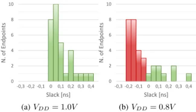
However, DVAS has a major drawback when combined with a standard ASIC implementation flow. Indeed, synthesis tools optimize timing-critical paths of an operator (i.e., paths with smallest slack) for performance, whereas less critical (largest slack) paths are exploited for area and power optimization. As a result, the delay of non-critical paths increases, to the point where their slack is comparable to that of critical ones, causing the so-called wall-of-slack [15]. An example is shown in Figure 1a, which shows the slack histogram of the endpoints of a 16x16-bit multiplier. The histogram is obtained after P&R, at the nominal implementation supply voltage (1V ).
0 2 4 6 8 10 -0,3 -0,2 -0,1 0 0,1 0,2 0,3 0,4 N. o f En dp o in ts Slack [ns] (a) VDD= 1.0V 0 2 4 6 8 10 -0,3 -0,2 -0,1 0 0,1 0,2 0,3 0,4 N. o f En dp o in ts Slack [ns] (b) VDD= 0.8V
Fig. 1: Endpoint slack histogram for a 16x16-bit multiplier. The effect of the wall-of-slack on DVAS is that the input dynamic usable without incurring in timing violations de-creases rapidly when VDD is scaled. As an example, Fig. 1b
shows the multiplier endpoint slack histogram, after the supply voltage has been downscaled to 0.8V . Red bars correspond to endpoints violating timing constraints. The large percentage of violating paths indicates that the input dynamic must be reduced significantly in order to restore timing compliance. Conversely, to obtain high-accuracy configurations, VDDmust
be kept to a value very close to the nominal one.
Moreover, when multiple DVAS operators in the same design must work in independent accuracy modes, every unit must be placed in a separate voltage domain. In MOS technology, voltage domains must be separated inserting level shifters, which introduce significant power overheads.
C. UTBB FDSOI and Back-Biasing
The proposed solution to overcome the limitations of DVAS is demonstrated on 28nm Ultra-Thin Body and Box (UTBB) FDSOI technology [16]. For the purposes of this paper, the most important characteristic of this technology is the wide applicable Back Biasing (BB) voltage range, spanning more than 2V , thanks to the presence of the Buried Oxide (BOX) layer, which acts as back-gate and removes body-source P/N junctions. Compared to the conventional range for bulk tech-nology’s Body Biasing (±300mV ), FDSOI Back Biasing has a stronger impact on Vth, and in turn on the performance/power
tradeoff. Forward Back Biasing (FBB) allows to lower Vthand
reduce the switching delay of a transistor, at the expense of an increase in sub-threshold leakage currents. Reverse Back Biasing (RBB) has the opposite effect. In both cases, the body factor (i.e., the sensitivity of Vth to BB) is as high as
85mV /V [17]. One issue when using BB is that deep N-Well areas of the circuit with independent BB voltage must be separated by means of guardbands, which introduce area overheads. This makes independent control of Back Biasing to single devices impractical. Conversely, devices with common Back Bias must be grouped into geometrically localized BB domains (or islands). In our technology node, the minimum BB domain guardband width is about 3.5µm, a value compa-rable to the height of the standard cells (1.2µm).
III. BACKBIASING FORADEQUATECOMPUTING The key limitation of DVAS with respect to the wall-of-slack is that when VDD is lowered, the entire operator timing is
slowed-down. This is clearly a problem when different parts of the circuit require different speeds (and hence a different power consumption), and in particular, as shown later, when the accuracy “modes” of an operator are implemented through reduction of input bitwidth (as in DVAS).
One possible solution to selectively tune the delay of different parts of the circuit would be to partition it in multiple independent supply voltage islands. However, due to the large overheads, this solution is only feasible at the SoC-level, and not at the fine granularity required for the relatively small hardware operators considered in this work; in particular, the insertion of level shifters between domains would have a relevant impact on power consumption [18].
Thus, in this paper we propose a methodology to achieve such selective tuning of the power/accuracy tradeoff using dynamic threshold voltage (Vth) scaling by means of Back
Biasing (BB). As described in Section II-C, BB domains require a small separation guardband but no level shifters, and thus have a much smaller power overhead compaed to supply voltage domains. Nevertheless, independent assignment of bias voltages to individual cells is obviously unfeasible; instead, to admortize the area overheads, groups of topologically close cells must share a common BB. Given the similarity between the size of separators and the height of a cell, the minimum size of these regions should be in the order of a few tens of rows of the placed design. Therefore, in our methodology, the circuits are partitioned in Vthdomainsor islands. Each domain
has an independent BB control, whereas the entire operator shares a single VDD. The additional Vthknob is leveraged to
speedup only timing critical parts of the circuit.
In this work we consider only two possible distinct Vth
assignments to domains: Standard Vth (SVT) as the nominal
condition, and Low Vth(LVT) as the “boosting” condition. In
28nm UTBB FDSOI technology, we map SVT to No Back-Bias (NoBB) and LVT to Forward Back-Back-Bias (FBB). This simplifies both the search for the optimal Vth assignment to
domains, as well as the generation of Back Bias voltages in the final circuit. In particular, two DC-DC converters (e.g., charge pumps) can be used to generate FBB voltages (for N-Well and P-Well) and some power switches to selectively connect the
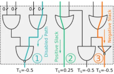
Disabled P ath 0 0 0 0 TS=-0.5 TS=0.25 Positive Slack TS=-0.5 TS=-0.5 Negative Slack 1 2 3
Fig. 2: Timing paths in an operator working with reduced bitwidth. Zeroed inputs are marked with a 0. Each output is associated a slack TS computed assuming a clock period of 1
“unit”, and that all gates have a delay of 0.75 units.
Well pins of each domain either to the converters output or to ground. Our methodology can however be applied to more than two Vth values, as well as to other forms of Vth tuning (e.g.,
Body Biasing bulk CMOS). Moreover, it is worth emphasizing that our approach is not alternative but rather complementary to DVAS; it is possible to set a given VDD for the entire
operator and then use BB to fine-tune the consumption and speed of different parts of the circuit.
While runtime BB assignment to affect circuit speed has been already exploited in literature for other reasons [17], we apply this principle to a completely new objective, i.e., optimizing the power consumption of a hardware operator based on runtime-varying accuracy requirements. We will later show the relevance of this objective on the methodology.
A. Runtime Accuracy Scaling
In our methodology, runtime adaptation of the operators ac-curacy is obtained using the same principle of DVAS [14]: depending on the required accuracy, some LSBs of the opera-tor inputs are simply set to zero. In this paper we focus on the design of individual operators, and we assume that the number of zeroed LSBs is specified by means of external control signals. The selection of the optimal accuracy is determined at application level, and is outside the scope of this work. Clamping some input LSBs at zero has an obvious effect on the timing paths that have those inputs as source points, which become deactivated (labeled with 1 in Figure 2). The remaining active paths in the circuits include as usual paths with positive slacks ( 2 ) and with negative slacks ( 3 ). These sets depend on the selected input width as well as on the global VDD. Ideally, dynamic Vth assignment by means
of BB should be used to speed-up only critical paths ( 3 ), leaving the other two sets in low-speed/low-leakage state. B. Partitioning of the operator into Vth/BB Domains
As already mentioned, BB cannot be applied at an arbitrarily fine granularity; the maximum number of Vthdomains NM AX
must be determined based on the acceptable area overheads, and traded off with the benefits in terms of power saving. Once NM AX is defined, however, there are still many degrees
of freedom available regarding the possible shapes of the Vth
domains. The definition of these regions is a fundamental issue in the proposed methodology. The basic problem of partitioning a circuit into multiple regions for selective ap-plication of a knob (Vthtuning, in our case) to control some
design tradeoffs (power/accuracy, in our case) has been already studied the literature for various knobs and tradeoffs [20].
An important issue in the partitioning process is its impact on the other figures of merit of the circuit (timing, dynamic power consumption, etc.), due to the fact that Vth domains
are physically isolated regions in the die. Indeed, cells should be kept as close as possible to their optimal position (i.e., the one determined by a standard placement algorithm) in order to minimize the impact on timing and power.
In addition to these traditional constraints, our problem intro-duces a new relevant element of complexity in the partitioning. In fact, adequate operators must work in multiple accuracy configurations (i.e., input bitwidths). The ideal goal would be to optimize power consumption in all these configurations. However, each of them imposes different constraints on the optimization, due to the impact of zeroed LSBs on timing paths described in Section III-A. Determining a single physical partitioning that is optimal for different bidwidths is not trivial; since each accuracy mode implies a different set of critical paths, a solution that is optimal, (i.e., that allows to speed up only the critical paths) for a given input bitwidth, might not be optimal for another bitwidth.
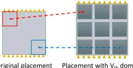
In this work, our objective is to show a proof-of-concept of the usability of dynamic Back Biasing for adequate computing. Therefore, we do not investigate complex partitioning algo-rithms; we rather consider the simplest possible partitioning of a die into NM AX sub-blocks, that is, a regular grid of Vth
domains. Each of the NM AX domains is assigned an identical
area of rectangular shape, equal to a fraction 1/NM AX of
the total; Figure 3 shows an example for NM AX = 9. This
solutions has the desirable property of a regular structure which eases the physical implementation [19]. Moreover, it minimizes the overheads in terms of timing and power at maximum accuracy (i.e., full bidwidth), since none of the cells are displaced in order to be assigned to a Vth domain. The
drawback of a regular tiling is that it might fail to isolate gates belonging to the paths that require speedup for a given bitwidth (i.e., set 3 in Figure 2). Thus, cells that do not need speed-up might end up in the same domain of cells that must be boosted. In this case, in order to meet timing constraints, the entire domain has to be assigned to LVT/FBB, resulting in a power overhead. However, due to the small granularity of Vthdomains, this overhead will be much smaller with respect
to that of raising VDD in DVAS.
C. Implementation Flow
Figure 4 shows the proposed fully automated flow for the implementation of adequate operators based on Vth scaling.
The flow consists of two main parts. The first implementation phase(green background in the figure), consists in the physical design of the operator. The result of implementation then undergoes a second optimization phase (blue background), in which the goal is determine the best assignment of the technological knobs for each bitwidth of interest.
The implementation phase takes as input a gate-level netlist of the original (accurate) circuit. The first step consists in performing a standard placement of the operator at nominal voltage, without Vth domains. In this step, the cells of the
operator are placed according to “standard” constraints (i.e., timing, area and power) as determined by the P&R tool.
Original placement Placement with Vthdomains
Fig. 3: Regular Grid Partition that identifies the Vthdomains.
First Placement (no BB Domains) Insertion of Vth Domains Incremental Placement Netlist (.v/.vhd) Parasitics (.spef) Netlist(.v) STA (Filter) Power Analysis Optimal Conf. ∀bitwidths Ca de nc e SoC En co un te r Synopsys PrimeTime Conditions (NMAX, NVDD, B) ∀Design Points Violation?No Yes
Fig. 4: Implementation Flow.
Then, the silicon area is enlarged in order to accommodate the separation guardbands, using the regular grid partitioning described in Section III-B, and depending on the desired num-ber NM AX of Vthdomains. Finally, an incremental placement
step is executed. In this step, the tool takes into account the newly inserted Vth domains and their possible operating
modes (NoBB or FBB), and consequently modifies gate sizing, position, etc., in order to meet all timing (setup and hold) and DRC constraints. The tool is also instructed to insert Well Taps for the connection of Back Bias voltage rails to the different domains. Finally, the implementation is completed with routing. The outputs of the implementation phase are the placed and routed netlist of the operator, including Vth
domains, and the corresponding parasitics file.
These results are then fed to the optimization phase, in which an exhaustive exploration of all possible operating conditions is performed. Specifically, the circuit is analyzed for all possible combinations of (i) VBBassignments (NoBB or FBB)
to the NM AX domains and (ii) input bitwidths. Moreover,
when our approach is combined with DVAS, the analysis of each point is repeated at multiple values of the global VDD.
The overall complexity of the exploration is O(2NM AX · B · NVDD), where B is the range of bitwidths of interest, and NVDD is the number of supply voltages to be explored. These values are all relatively small, making exhaustive exploration feasible. NM AX is in the order of a few tens; B in the
worst case coincides with to the full bitwidth (16 or 32) but is typically smaller; NVDD depends on the resolution of the supply voltage generator and the allowed range of variation of VDD: assuming a 100mV step and a range between 0.6V and
1.0V, NVDD = 5. With these values, the number of points to consider is in the order of some thousands. Furthermore, points that are unfeasible can be easily filtered out without the need of a complete analysis. Unfeasibility is checked by running
0.00E+00 5.00E-04 1.00E-03 1.50E-03 2.00E-03 2.50E-03 0 2 4 6 8 1 0 1 2 1 4 1 6 PO W ER C O N SU M PT IO N [W ] ACCURACY [BITS] Proposed Method (2x2 Domains) DVAS (NoBB) DVAS (FBB)
(a) Booth Multiplier
2.00E-03 4.00E-03 6.00E-03 8.00E-03 1.00E-02 1.20E-02 0 2 4 6 8 1 0 1 2 1 4 1 6 PO W ER C O N SU M PT IO N [W ] ACCURACY [BITS] Proposed Method (3x3 Domains) DVAS (NoBB) DVAS (FBB) (b) FFT Butterfly 1.00E-03 2.00E-03 3.00E-03 4.00E-03 5.00E-03 6.00E-03 7.00E-03 8.00E-03 9.00E-03 1.00E-02 0 2 4 6 8 1 0 1 2 1 4 1 6 PO W ER C O N SU M PT IO N [W ] ACCURACY [BITS] Proposed Method (3x3 Domains) DVAS (NoBB) DVAS (FBB) (c) FIR Filter
Fig. 5: Comparison with DVAS in terms of bitwidth versus power tradeoff.
Design A [mm2] f
clk[GHz] Groups Aovr[%]
Booth 2.59 · 10−3 1.25 2x2 15 Butterfly 7.71 · 10−3 1.00 3x3 17
FIR 9.10 · 10−3 0.75 3x3 16
TABLE I: Post P&R design characteristics and groups config-urations for DVAS comparison.
Static Timing Analysis (STA) on the netlist; if it incurs in a timing violation, that point is discarded. For instance, the all-NoBB configuration with VDD= 0.6V will very likely be not
timing compliant at maximum accuracy. STA is quite fast (in the order of 0.1s for the scale of our operators), and even faster for lower accuracy netlists, where some paths become inactive after shrinking the bitwdith. On average, we have observed that about 75% of the configurations are filtered by STA.
Feasible configurations are instead analyzed for power, taking into account both leakage and dynamic components. This phase can optionally use realistic inputs for switching activity annotation. For each accuracy (i.e., bitwidth) of interest, the operating condition that produces the minimum power con-sumption is stored. The corresponding knob configurations (VBBassignment to the different domains, and possibly global
VDD value) are output for each bitwidth of interest. Power
estimation including importing of VCD traces takes about 1s on our server (Intel Xeon [email protected], 128GB DDR3).
IV. EXPERIMENTALRESULTS A. Experimental Setup
To evaluate the effectiveness of our method, we applied it to three different hardware designs common in DSP applications, which are typically error tolerant but often have time-varying accuracy requirements: a Booth multiplier with Wallace tree, a 30-tap FIR filter, and a butterfly unit, i.e., the main datapath component of a FFT accelerator. We considered 16-bit fixed-point implementations of the operators (larger bit-widths are seldom used in this type of applications).
We started from behavioral specifications of the operators in VHDL or Verilog. For synthesis and implementation we tar-geted a 28nm FDSOI standard-cell library from STMicroelec-tronics. We used Synopsys DC-I-2013.12-SP4 for synthesis and Cadence Innovus v15.13 for P&R. Post implementation
netlists and parasitics have been loaded in Synopsys PT-I-2013.12-SP1 for timing and power analysis. A summary of the post-P&R characteristics of the three designs is reported in Table I, where A represents the silicon area and fclkis the
nominal clock frequency used for synthesis. For all operators, we used a nominal supply voltage VDD= 1.0V .
Notice that, in order to fully exploit the flexibility of our method, it is preferable that the maximum accuracy mode at nominal VDD corresponds to a fully-boosted configuration of
the domains. Thus, during this first P&R of the three operators without Vth domains, we considered a standard-cell library
characterization in which all cells are in FBB state. B. Comparison against DVAS
DVAS was already shown to provide better results than tradi-tional architectural solutions for adequate hardware operators design ( [10], [13], etc.). Therefore, we limit the comparison of our method against DVAS. We implemented both methods on the three target designs. The selected configuration of Vth
domains is shown in Table I, together with the area overhead Aovh introduced by separation guardbands. For both DVAS
and our method we fixed the clock frequency at the nominal value of Table I, and we considered 5 VDD conditions, from
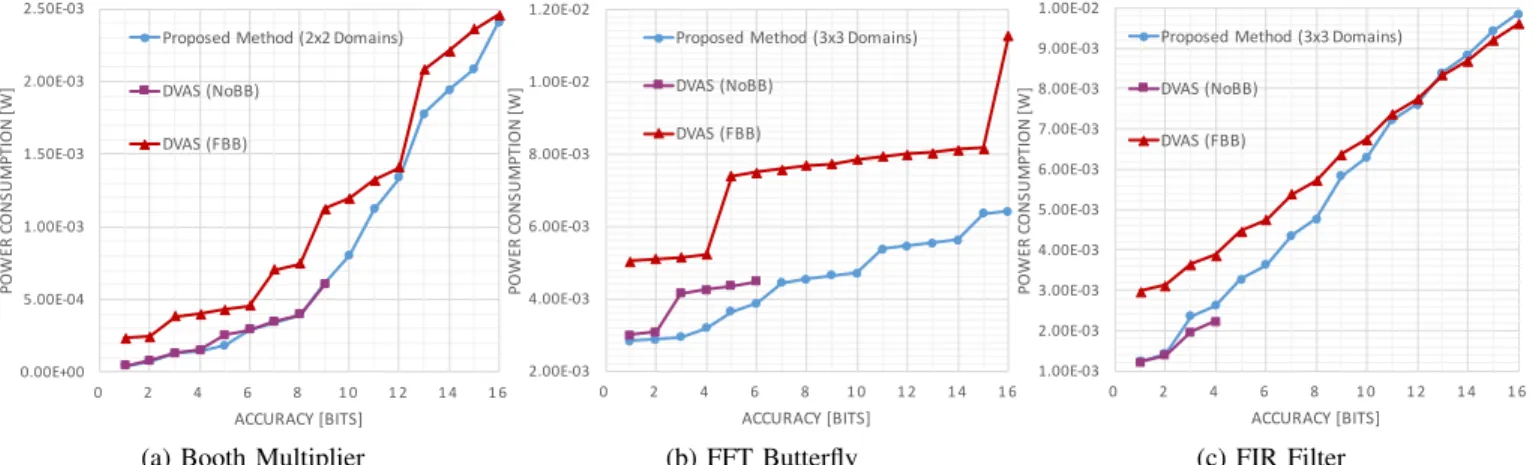
1.0V (nominal) to 0.6V , in steps of 0.1V . We used a BB voltage of ±1.1V (N-Well/P-Well) as FBB condition. Figure 5 shows the results of the comparison on an bitwidth versus power consumption plane. Each curve is a Pareto frontier, i.e., it shows the minimum power configuration for each bitwidth, considering all possible combinations of VDD
and (for our method) Vth assignment. The graphs contain
only configurations that fully meet timing constraints, taking into account disabled paths due to reduced dynamic. Power includes both leakage and dynamic components. As explained in Sec. IV-A, the original operators were implemented using FBB as nominal condition. Thus, for a fair comparison, Figure 5 reports both the result of DVAS with NoBB, and that of DVAS with FBB (i.e., boosting all cells of the operator). A first important observation is that DVAS with NoBB, i.e., the standard implementation reported in [14], cannot reach maximum accuracy: the curves are limited to very small bitwidths in all three cases, indicating there is no solution for higher bitwidths at that frequency. Under the same timing
0,00E+00 5,00E-04 1,00E-03 1,50E-03 2,00E-03 2,50E-03 3,00E-03 8 9 10 11 12 13 14 15 16 Po w er Consu mp tion [W] Accuracy [bits] 1x2 2x1 1x3 3x1 2x2 3x3
(a) Power consumption at different accuracies
0 5 10 15 20 25 30 35 1x2 2x1 1x3 3x1 2x2 3x3 Ar ea Ov er head [%] Configuration (b) Area overhead
Fig. 6: Power saving and area overhead for different numbers and configurations of Vth domains in the Booth Multiplier.
constraints, our method can instead reach maximum accuracy for all designs. DVAS with FBB, conversely, can work at maximum accuracy for all three designs; however, due to the wall-of-slack, the power vs. bitwidth tradeoff is significantly worse with respect to our method. For multiplier and FIR, the overheads of DVAS are particularly evident looking at the “step-wise” shape of the Pareto frontier, in which each step corresponds to a change of VDD. At 10-bit, the power
saving of our method with respect to DVAS is 32.67% for the Booth and 39.92% for the FIR. For what concerns the butterfly, the more linear curves of DVAS show that this unit is less affected by the wall-of-slack, and consequently the improvement thanks to Back Biasing is less marked. Nevertheless, it is still possible to obtain a 16.5% power saving with respect to DVAS at 8-bit.
The only case in which DVAS yields (marginally) better results than our approach is for the butterfly, at very small or very large (close to the maximum) bitwidths. These are due to the incremental placement after insertion of Vth domains. The
same overheads are not visible for Booth and FIR, mainly because the impact of guardbands is smaller (the Booth has a smaller number of domains, and the FIR has a larger area).
C. Impact of the number ofVth domains
The number of Vthdomains has a strong impact on all figures
of merit in our method. Figure 6 depicts this effect using the Booth multiplier as an example. Figure 6a shows the power savings in different accuracy modes for different groups con-figurations. For visualization purposes, the graph only reports accuracy modes between 8 and 16 bits (those < 8 bits are seldom needed in realistic applications). Increasing the number of groups produces a general reduction in power consumption, especially at high accuracy modes. This is expected, as more groups allow a finer-grain selection of the parts of the operator to be sped up. However, this trend is not always respected; for particular accuracy conditions, increasing the number of groups has a negative effect on power (e.g. 2x1 versus 3x1 at 10-bits accuracy). This is due to the addition of guardbands between groups, which may cause operator cells that were previously closer to move away from each other, extending the corresponding routes. Figure 6b reports the area overheads due to guardbands for the groups configurations analyzed.
Expectedly, area increases with the number of groups, while the dependence on the structure has a less evident effect. As a general observation, it is evident that the selection of the number of Vth domains strongly depends on the metrics of
interest. In general, the power reduction in accuracy modes of interest must be balanced with the area budget. However, since our method is automated, the design space can be explored exhaustively, at least for a small number of groups (≤ 10).
V. CONCLUSIONS
In this paper, we have presented a novel method for the implementation of adequate hardware operators. Thanks to the flexibility provided by the additional Vth knob, this method
achieves significantly larger power savings at iso-accuracy compared to the previous DVAS, at the price of a small area overhead. Moreover, it removes the need for level shifters in complex systems including multiple operators. Future devel-opments include the study of alternative Vthdomains
construc-tion methods, and an investigaconstruc-tion of the optimal number and configuration of domains.
REFERENCES
[1] V. Chippa et al, “Analysis and characterization of inherent application resilience for approximate computing,” in Proc. DAC 2013, pp. 1–9. [2] Q. Xu, N. S. Kim, and T. Mytkowicz, “Approximate computing: A
survey,” IEEE Design & Test, vol. 33, no. 1, pp. 8–22, 2016. [3] H. Jiang, J. Han, and F. Lombardi, “A comparative review and evaluation
of approximate adders,” in Proc. GLSVLSI 2015, pp. 343–348. [4] K. Y. Kyaw, W. L. Goh, and K. S. Yeo, “Low-power high-speed
multiplier for error-tolerant application,” in Proc. EDSSC, 2010, pp. 1–4. [5] J. Huang, J. Lach, and G. Robins, “A methodology for energy-quality tradeoff using imprecise hardware,” in Proc. DAC 2012, pp. 504–509. [6] F. Farshchi, M. S. Abrishami, and S. M. Fakhraie, “New approximate
multiplier for low power digital signal processing,” in Proc. CADS 2013, pp. 25–30.
[7] A. Lingamneni et al, “Synthesizing parsimonious inexact circuits through probabilistic design techniques,” ACM Trans. Embed. Comput. Syst., vol. 12, no. 2s, pp. 93:1–93:26, May 2013.
[8] A. Verma, P. Brisk, and P. Ienne, “Variable latency speculative addition: A new paradigm for arithmetic circuit design,” in Proc. DATE 2008, pp. 1250–1255.
[9] A. Kahng and S. Kang, “Accuracy-configurable adder for approximate arithmetic designs,” in Proc. DAC 2012, pp. 820–825.
[10] M. de la Guia Solaz, W. Han, and R. Conway, “A flexible low power dsp with a programmable truncated multiplier,” IEEE Trans. on CAS I, vol. 59, no. 11, pp. 2555–2568, Nov 2012.
[11] R. Ye et al, “On reconfiguration-oriented approximate adder design and its application,” in Proc. ICCAD 2013, pp. 48–54.
[12] D. Mohapatra et al, “Design of voltage-scalable meta-functions for approximate computing,” in Proc. DATE, 2011, pp. 1–6.
[13] C. Liu, J. Han, and F. Lombardi, “A low-power, high-performance approximate multiplier with configurable partial error recovery,” in Proc. DATE2014, pp. 95:1–95:4.
[14] B. Moons and M. Verhelst, “Dvas: Dynamic voltage accuracy scaling for increased energy-efficiency in approximate computing,” in Proc. ISLPED2015, pp. 237–242.
[15] A. Kahng et al. “Slack redistribution for graceful degradation under voltage overscaling,” in Proc. ASP-DAC 2010, pp. 825–831.
[16] P.-E. Gaillardon et al, “A survey on low-power techniques with emerging technologies: From devices to systems,” J. Emerg. Technol. Comput. Syst., vol. 12, no. 2, pp. 12:1–12:26, Sep. 2015.
[17] E. Beign´e et al, “A 460 mhz at 397 mv, 2.6 ghz at 1.3 v, 32 bits vliw dsp embedding f max tracking,” IEEE Journal of Solid-State Circuits, vol. 50, no. 1, pp. 125–136, Jan 2015.
[18] J. Hu et al, “Architecting Voltage Islands in Core-based System-on-a-chip Designs,” Proc. ISLPED 2004, pp. 180–185.
[19] T. Kutzschebauch and L. Stok, “Regularity Driven Logic Synthesis”, Proc. ICCAD2000, pp. 439–446.
[20] K. Usami and M. Horowitz, “Clustered Voltage Scaling Technique for Low-power Design”, Proc. ISLPED 1995, pp. 3–8.