HAL Id: lirmm-01708599
https://hal-lirmm.ccsd.cnrs.fr/lirmm-01708599
Submitted on 27 Mar 2019
HAL is a multi-disciplinary open access
archive for the deposit and dissemination of
sci-entific research documents, whether they are
pub-lished or not. The documents may come from
teaching and research institutions in France or
abroad, or from public or private research centers.
L’archive ouverte pluridisciplinaire HAL, est
destinée au dépôt et à la diffusion de documents
scientifiques de niveau recherche, publiés ou non,
émanant des établissements d’enseignement et de
recherche français ou étrangers, des laboratoires
publics ou privés.
GREAT: HeteroGeneous IntegRated Magnetic
tEchnology Using Multifunctional Standardized sTack
Mehdi B. Tahoori, Sarath Mohanachandran Nair, Rajendra Bishnoi, Sophiane
Senni, Jad Mohdad, Frédérick Mailly, Lionel Torres, Pascal Benoit, Pascal
Nouet, Rui Ma, et al.
To cite this version:
Mehdi B. Tahoori, Sarath Mohanachandran Nair, Rajendra Bishnoi, Sophiane Senni, Jad Mohdad,
et al.. GREAT: HeteroGeneous IntegRated Magnetic tEchnology Using Multifunctional
Standard-ized sTack. ISVLSI: International Symposium on Very Large Scale Integration, Jul 2017, Bochum,
Germany. pp.344-349, �10.1109/ISVLSI.2017.67�. �lirmm-01708599�
GREAT: heteroGeneous integRated magnetic
tEchnology using multifunctional standardized sTack
M. Tahoori1,S.M. Nair1,R. Bishnoi1,S. Senni2, J. Mohdad2, F. Mailly2, L. Torres2, P. Benoit2,P. Nouet2, R. Ma3, M. Kreißig3, F. Ellinger3,K. Jabeur4,P. Vanhauwaert4,G. Di Pendina4 andG. Prenat4
1)
Karlsruhe Institute of Technology, Germany
2)LIRMM, UMR CNRS 5506, University of Montpellier, France 3)
Technische Universität Dresden, 01069 Dresden, Germany
4)Univ. Grenoble Alpes, CNRS, CEA, INAC-SPINTEC, F-38000 Grenoble, France
Abstract— To tackle the key issues of monolithic heterogeneous integration, fast yet low power processing, high integration density, fast yet low power storage, the goal of the GREAT project is to co-integrate multiple functions like sensors (“Sensing”), RF receivers (“Communicating”) and logic/memory (“Processing/Storing”) together within CMOS by adapting the STT-MTJs (Magnetic devices) to a single baseline technology enabling logic, memory, and analog functions in the same System-on-Chip (SoC) as the enabling technology platform for Internet of Things (IoT). This will lead to a unique STT-MTJ cell technology called Multifunctional Standardized Stack (MSS). The major outputs of GREAT are the technology and the architecture platform for IoT SoCs providing better integration of embedded & mobile communication systems and a significant decrease of their power consumption. Based on the STT-MTJs (now viewed as the most suitable technology for digital applications and with a huge potential for analog subsystems) unique set of performances (non-volatility, high speed, infinite endurance and moderate read/write power), GREAT will achieve the same goal as heterogeneous integration of devices but in a much simpler way since the MSS will enable different functions using the same technology.
Keywords—Magnetic Tunneling Junction, Spin Transfer Torque, IoT
I. INTRODUCTION
Billions of Smart Connected Devices are sold every year with an increase of both the number and complexity for these systems. The interest for developing smart connected systems (Smart Sensors, Secure Elements, etc) based on an “Internet of Things” (IoT) is growing fast. The number of Internet-connected devices surpassed the number of human beings on the planet in 2011, and by 2020, Internet-connected devices are expected to number between 26 billion and 50 billion. New applications in IoT will require storing and computing ever-increasing amounts of data in battery-powered systems. The main components of IoT devices are autonomous battery-operated smart embedded systems comprising communication circuits, sensors, computing/processing devices as well as integrated memories. These smart connected devices embed RF circuits for communications, digital circuits for data processing, memory for data storage as well as analog circuits such as sensors, filters, converters, not to mention cameras, GPS systems etc. In battery-operated Machine to Machine (M2M) and Machine to Human (M2H) operations, the key processing cycle includes following steps: sleep, wake-up, sense, store, process, and send. Therefore, the enabling technology for IoT should provide 1) ultra-low power, 2) high performance processing, 3) fast, dense, and low power storage, and 4) heterogeneous integration based on “More than Moore” to enable different digital and analog functionalities. The
different functions are so far implemented in separate chips and/or fabricated using different technologies, which is a bottleneck in terms of costs and miniaturization. Heterogeneous monolithic integration of these different functionalities on a single chip is a key requirement for future IoT System-on-Chip (SoC) platforms.
A Non-Volatile Memory (NVM) based technology that would allow realizing digital, RF and analog functions on the same chip could enhance the integration and reduce the cost for the fabrication of high-end embedded platform for smart connected IoT systems, push forward their miniaturization, decrease their power consumption (by reducing the power consumptions of memory and sensor interfaces blocks by x5 or x10), enhance their security and improve their reliability while meeting the high performance requirements. Besides IoT, such a technology has also several applications in other energy-constraint high-performance embedded devices such as those used in telecommunications and smartcards, since these share many components with IoT systems with similar constraints and demands.
Based on a system-level approach, GREAT project will provide the enabling technology and architecture for high-end battery-operated IoT hardware platforms. At the technology level, it achieves the same goal as heterogeneous integration of devices but in a much simpler way since the same core technology (i.e. magnetic stack) will enable different functions. At the architecture level, the NVM-based normally off computing enables energy-efficiency, large storage, and high performance demands of high-end IoT platforms. The solution offered by GREAT promises to be superior to other heterogeneous integration alternatives, such as 3D, for such application domains. Because of that, GREAT has also several applications in other energy-constraint high-performance embedded systems such as those used in smartcards and telecommunications, as these share many components with such highly integrated IoT SoCs.
The rest of this paper is organized as follows. Section II discusses the common enabling technology for both analog and digital application. The process design kit is explained in Section III. Section IV is devoted to sensing and communication applications. Sections V and VI describe the digital memory subsystem and the cross-layer analysis framework for hybrid memory evaluation and variation analysis, respectively. Finally Section VII concludes the paper.
II. ENABLING TECHNOLOGY:MULTIFUNCTIONAL
STANDARDIZED STACK (MSS)
One of the major roadblocks is the availability of Non Volatile Memories (NVM) that would combine high speed,
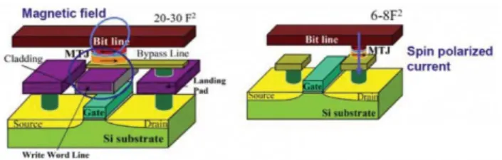
high density, and high endurance. Among the various emerging NVM technologies, MRAM has a unique set of performance, in particular in its Spin Transfer Torque (STT) implementation which combines non-volatility, high speed, high endurance and moderate read/write power (Figure 1). Several generation of MRAM exist according to the writing scheme. The so-called STT-MRAM in which writing is performed by a simple bipolar current pulse through the tunnel junction is the most promising technology, in particular for advanced technology nodes. The memory bit cell in this case becomes very simple (a MTJ in series with a transistor, cf. Figure 2), which promises high densities (<10 F²). The write cycle can be done in few ns, and scaling is possible until at least the 16 nm technology node. In addition the endurance (number of read/write cycles) is much greater than that of Flash memory (>1015 cycles) and retention
of information is well over 10 years.
Fig. 1. Comparison of the STT performances with the main existing memories
The building block of MRAM is the Magnetic Tunnel Junction (MTJ). It is a multilayered nanostructure whose resistance depends on its magnetic state. In its MRAM implementation it behaves as a bistable element that can be used for memory and/or logic functions (“processing/storing”). The MTJ, however, can also be used as a variable resistance for analog applications, including magnetic field or current sensor (“sensing”). Finally, it is also currently explored as an oscillating RF emitter or receiver source (“communicating”), therein covering a large fraction of the digital and analog subsystem chain of system communications devices.
Fig. 2. MRAM basis. Left :Former field-driven MRAM;Right : STT-MRAM
Up to now these different functions have been achieved separately, using dedicated optimized magnetic tunnel junctions stacks. However they are all based on similar STT-MTJs, differing only by some technology parameters. The idea of GREAT project is to adapt the STT-MRAM to a single baseline technology allowing performing logic and analog functions in the same SoC. This will lead to a unique STT-MRAM MTJ cell which we call Multifunctional Standardized Stack (MSS). The basic idea consists of using a standard perpendicular STT-MTJ in memory mode with additional permanent magnetic biasing layers acting as magnets around it, to change its behavior for sensors or RF application. This
requires only one additional lithography step whose additional cost will be very low compared to the gain offered by the co-integration.
Therefore, this multifunctional standardized stack has to be designed and optimized to be the best compromise serving multiple functions, in order to integrate all of these functions “at once” without sacrificing performance of each function. For this purpose a standard perpendicular MTJ similar to those used in STT-MRAM devices will be employed together with additional permanent magnet biasing layers to enable other functionalities beside memory and logic. To achieve this, we intend to use out-of-plane MTJs for MSS, as those are currently optimized for STT-MRAM applications with RA in the range of 5 to 10Ω.μm². The perpendicular anisotropy in these MTJs originates from electronic hybridization at the magnetic metal/oxide interface, a phenomenon discovered in 2002 by one of the partner of this consortium [1].
For memory applications, MTJs can switch quite fast (ns time scale, have adjustable retention by playing with the diameter of the stack thus allowing to minimize the switching current according to the specified retention), and have very long endurance. For RF and sensor functions, the density is not a requirement since only a very limited number of sensors or RF oscillators are required per chip. We intend to add patterned permanent magnets (for instance made of CoCr alloy or NdFeB) on the two sides of the MTJ pillars as this is done to bias magnetoresistive heads in hard disk drives.
For the spin transfer oscillator, the size and shape of the permanent magnet biasing layer will be adjusted to produce a horizontal field in the order of half of the effective perpendicular anisotropy field (~1kOe) so that the free layer magnetization will be tilted at about 30°. This will allow the generation of a processional motion of the free layer magnetization on a cone of tilted axis thereby producing a RF voltage signal across the MSS stack.
For sensor applications, we will develop a sensor sensitive to the out-of-plane component of the field. First, the diameter of the pillar will be increased compared to the MSS used for memory functions. Besides, the size and shape of the permanent magnet biasing layer will be adjusted to produce a horizontal field slightly larger than the effective perpendicular anisotropy field (~2-3kOe) so that the free layer magnetization will be pulled in-plane by this biasing field. When submitted to an out-of-plane field to be sensed, the free layer magnetization will rotate upwards or downwards producing a resistance change proportional to the out-of-plane field amplitude.
III. CUSTOM CELL DESIGN FOR ANALOG AND DIGITAL APPLICATIONS
A. Micromagnetic simulations
While operational conditions for MRAM and magnetic sensor functions are well known for the targeted MSS stack based on a fully perpendicular magnetic tunnel junction, the conditions for inducing steady state excitations are less well known. The aim of this task is therefore to provide, via simulations, the conditions of field and current and potentially
other material parameters under which the steady state oscillations will be observed.
Fig. 3. (a) Static voltage-field diagram of states of free-layer magnetization calculated by taking into account the second order easy-axis magnetic anisotropy. The colour code shows the out of plane mz component of the free layer magnetization. The simulations have been performed for a temperature of 100K; (b) Dynamic voltage-field diagram of states of the free-layer magnetization. The colour code shows the power spectral density amplitude variation.
The preliminary results (Fig. 3) show that it is possible to obtain steady states precessions, but in a range of voltages which is relatively low for using the MSS as a RF emitter. Further investigations will be carried out to try to improve the parameters to reach this goal. On the other hand, the use of the MSS design as a RF receiver should be easier, since it does not require steady state precessions.
B. Compact model of the device
Fig. 4. Comparision of the compact model strategies: the first graph represents the pusle of writing current, whose amplitude is varied. The second one corresponds to the model based on LLG equations, where we can see the expected precessions of the switching and the last one shows the results of the model based on Neel-Brown’s and Suns’ theories. The models are tuned to give the same results in terms of switching durations
A compact model of the MSS device is required to perform electrical simulations of hybrid circuits. Two approaches are considered for the description of the magnetic behavior in an electrical compact model [2]:
x The first one is based on the Neel-Brown’s and Sun’s models, giving the typical switching duration as a function of the amplitude of the writing current pulse. This approach offers good performance in terms of simulation time and is particularly adapted for digital
circuits where MSS is used in switching mode, but not suitable for use in analog configurations (sensors or RF). x The second approach is based on LLG equations which
model the dynamics of the magnetization. It is suitable for all the modes of operations and can also represent the stochasticity of the MSS switching thanks to a noise module to be used in a transient noise electrical stimulation.
Both models has been developed (Fig. 4) in the framework of the project and will be ideally merged to a unified model.
C. Physical verification tools
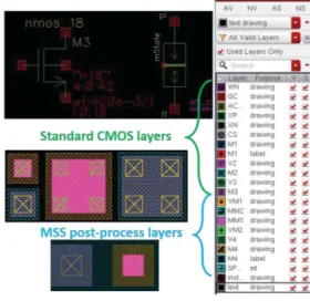
Once the circuit has been designed and successfully simulated, it is necessary to provide physical layout. This requires integrating the magnetic layers in the technology files used by the EDA tools. Once the layout is drawn, several physical verifications have to be carried out. First, the compliance of the layout with the design rules of the manufacturer has to be checked, i.e., Design Rules Checking (DRC). Then, the circuit has to be extracted, that is to say that the devices and their interconnections have to be identified from the layout. The extracted circuit can then be compared to the simulated circuit by a LVS (Layout Versus Schematic) operation. All these verifications require technology files giving information about the technology (design rules, technology parameters for extraction…) for the design suites. In the framework of GREAT project, we used a hybrid technology based on the CMOS 180nm technology from Tower. In this context, we have modified the technology file from the CMOS technology to integrate the magnetic front-end and back-end. A layout of the MSS device was provided, to be easily instantiated in a full layout, as well as some facilities add-ons like automatic vias generation and dummies filling for density purposes (Fig. 5).
Fig. 5. Layout facilities in the PDK: on the top left, the schematic of the MSS allowing to describe the circuit for electrical simulation. In the middle left, automatic via generation. In the bottom left, the layout of the MSS device and in the right, the Layer Selection Window in Cadence showing the additional layers for the magnetic post-process.
IV. COMMUNICATION, SENSING AND TUNING
A. Sensors
The linear and reversible dependence of the MTJ resistance with properly oriented magnetic fields will be exploited to design, fabricate and characterize MTJ based sensors. Several architectures will be proposed to address applications such as current monitoring (contactless power line monitoring), high-galvanic isolation voltmeters (fuel cells), and magnetic field measurement (electronic compass). All these architectures are useful to monitor most of IoT embedded systems applications.
The magnetic field will be used as a primary or secondary physical magnitude that affects linearly the resistance of the sensor. Front-End analog circuits will be designed on the same chip as the sensor itself to obtain smart sensors and to cope with main non-idealities such as offset, sensitivity, uncertainty and other mismatches. A particular effort will be put on the development of smart IC PADs able to monitor the current consumption of a SoC by integrating a magnetic field sensor close to the power line. Those smart power PADs will allow the implementation of efficient power management techniques in energy-constraint systems.
B. Analogue RF receivers based on MTJs
The main task is to realize the integration of MSS MTJs on top of CMOS PLLs and to demonstrate phase noise reduction of 10 dB at 100kHz offset frequency of the fully integrated PLL as compared to the standalone MSS. This integration will exploit knowledge of previously designed (standalone) PLLs for MTJs where modifications have to consider the specific dynamic properties of the MSS stacks (determining the useable frequency range (1 to 5GHz is aimed at), the frequency tuning, the free running phase noise, non-linear coupling) as well as the use of a different IC technology (requiring adaptations of the PLL amplifier, frequency divider, phase comparator, loop filter, voltage-current converter) [9]. In order to evaluate different types of PLL configurations and to determine the optimized one, several runs will be required.
For frequency detection, the different detection schemes will be tested off chip and their performance evaluated with respect to sensitivity (output to input power), frequency resolution, signal stability and signal to noise ratio. Requirements for integration will be established and assessed in terms of pre- and post-amplification of input and output signals, DC current biasing circuit, footprint, depending on the output the consortium will decide to launch a run for testing integration schemes.
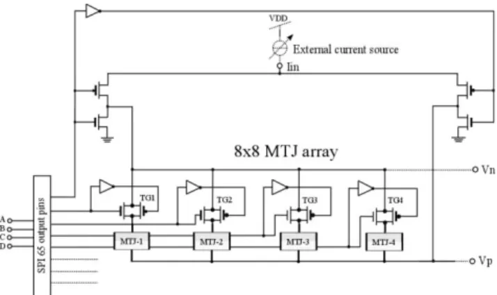
We have taped out an 8x8 MTJ switch array to be used for the PLL as an RF signal source as well as for the frequency detection as an RF to DC convertor (Fig. 6). Based on simulation results and practical experiences with the MTJs, we obtained the MTJ parameters, with which we decided to use 1.8V CMOS transistors for the switch implemented as a transmission gate (TG). According to the simulations, this TG switch can have more than 0 dB gain over 1 to 5 GHz. The on-off state of each TG and its MTJ is controllable through an integrated serial peripheral interface (SPI). The bottom and top sides of the array are connected to two CMOS push pull structures respectively. The top side (port Iin) of the two push
pull structures will be connected to an external sourcing current source. The direction of the current that will flow through the selected MTJ can be also defined via the integrated SPI.
Fig. 6. Schematic view of the designed 8x8 MTJ switch array
C. MSS-controlled digital tuning circuits for analog IPs
Bistability and non-volatility of MSS will be exploited to develop a family of tunable functions. This task will explore compensation and tuning architectures in the form of digital potentiometers or digitally-programmable current sources, controlled by MSS-based registers, to obtain an electrical non-volatile tuning that could be modified in-field to take into account ageing of the circuit. This ability being a real added value with respect to standard techniques in CMOS processes. A complete set of functions with non-volatile tuning will be proposed: voltage references, current sources, tunable Operational Transconductance Amplifier, and so on. After feasibility evaluation, a set of demonstrators are under fabrication and will be characterized. Validated functions will then be transferred with proper documentation and models for IoT system integration in the project. Some dedicated mixed (analog/digital) functions for secure elements will be addressed into this task, for instance PUF or TRNG function could be defined and designed to be part of the final IoT demonstrator.
Fig. 7. Impact of process variations on a basic current source (red bars on the left graph) and after calibration using a 4-bits tunable current source (blue bars on the left graph). Closed view of current variations after calibration (blue bars on the right graph).
In order to improve the robustness of analogue IPs against process and mismatch variability the work focuses so far on exploring compensation and tuning architectures. We studied tuneable functions thoroughly such as a programmable current source and a programmable transconductance amplifier. For each function, different architectures have been compared on
±15%
±3 Imean
< ±1.5%
both yield and surface aspects based on electrical simulations. We also developed a simulation environment for evaluating post-process digital tuning of these IPs. We obtained encouraging results showing that the variability is being reduced by a factor of 10 (Fig. 7). We also studied the limits of such tuneable architectures by focusing on noise and differential non-linearity (DNL) aspects, both of which add constraints on the design that should be taken in account. We put in place a simulation bench including the MSS-based registers in order to make use of the non-volatile memories that are available in this project. This aspect is really important to keep the tuned configuration over time.
V. HYBRID MEMORY DESIGN EXPLORATION FRAMEWORK
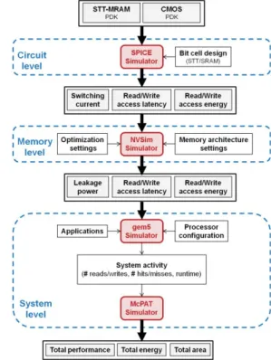
Exploring the impact of STT-MRAM on real systems requires a cross-layer investigation where device, circuit, memory, and system levels are taken into account. Such a simulation platform could be a fast and cost-effective solution to provide essential feedback to enhance the development of STT-MRAM devices. Moreover, this exploration framework would also give the possibility to evaluate hybrid designs by considering several memory technologies inside the system. This section details the cross-layer simulation environment considered in this EU project and the different exploration tools used to build an accurate exploration framework for performance, energy and area analysis of a full system-on-chip based on MRAM. Figure 8 describes the cross-layer simulation environment for hybrid design exploration.
A. Circuit level
First of all, a Process Design Kit (PDK) is developed with the device-level parameters, as discussed in Sec. III. This PDK is then used as an input for circuit-level simulation through SPICE. Thus, single bit cells and flip-flops based on MRAM, sense amplifiers, and write circuits can be analyzed.
B. Memory level
Memory-level evaluation is performed thanks to NVSim [3], a performance, energy, and area estimator for non-volatile memories (NVM) which uses an empirical modeling methodology based on the well-known CACTI [4]. Based on circuit-level data of single bit cell (Section A) and the desired memory architecture information such as capacity, data width, and type of memory (e.g. Cache, RAM, CAM), NVSim estimates the access time, the access energy, and the total area of a complete NVM chip. This tool also includes optimization settings (e.g. buffer design optimization) and various design constraints to facilitate the design space exploration before the fabrication of the actual NVM chip.
C. System level
Memory-level information is extracted from NVSim to explore the impact of different memory technologies at system level. An accurate performance simulator (gem5 [5]) is used to simulate a single-core or a multi-core architecture with its memory hierarchy. Gem5 generates a detailed report of the system activity including the number of memory transactions (e.g. number of reads/writes, number of hits/misses) and the execution time. This activity information is then used by McPAT [6], a power and area estimator tool at architecture
level. Extending the exploration framework with McPAT allows us to analyze not only the energy consumption related to the memory components, but also to evaluate the energy of the complete system including the processor cores, buses, and memory controller.
Fig. 8. Hybrid design exploration framework
VI. VARIABILITY ANALYSIS IN STT-MRAM
In previous section, we have presented a cross layer platform where the memory design parameters are evaluated based on their nominal values. These memory parameters can significantly vary under the influence of variations. The functionality of STT-MRAM is influenced by variations in CMOS components as well as by the magnetic fabrication process. The manufacturing imperfections in the magnetic devices disturb the magnetic properties of the cell such as switching characteristics, resistance differences, etc. Therefore, quantifying the effect of these variations at the memory architecture level is important for a realistic estimation for the performance, energy and reliability for STT-MRAM. To address this, we have developed a Variation Aware
Estimator Tool for STT-MRAM (VAET-STT) [7]. This is an
early stage design exploration tool for STT-MRAM, which considers process variation, stochastic switching and reliability requirements in its analysis and memory configuration optimization.
The VAET-STT tool is built on the top of NVSim [3] and extends it to account for variability in both the bit-cell and peripheral components. The impact of variability causes the latency and energy of the bit-cell and peripherals to follow distributions instead of being a single (nominal) value. The latency/energy distributions of the peripheral components, being CMOS based, is extracted by varying the transistor parameters based on Pelgrom model [8]. In the case of the
bit-cell read operation, the latency/energy distributions are obtained by executing Monte-Carlo SPICE simulations. On the other hand, for the bit-cell write operation, the latency samples for process variation is obtained from Monte-Carlo SPICE simulations. Then, we aggregate the stochastic distribution for each process variation sample to get the total bit-cell latency. These latency and energy samples obtained from the above models are then fit to known distributions. We observed that the bit-cell read latency follows an extreme value distribution whereas the bit-cell write latency follows a log-normal distribution. The bit-cell energies for both read and write operations follow normal distributions. Additionally, the latency/energy of the peripheral components also follows normal distributions.
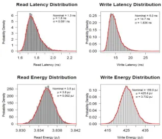
Fig. 9. Overall latency and energy distributions for a subarray size of 1024 rows x 1024 columns
These latency and energy distributions are then propagated to the next hierarchy levels in the memory architecture. In general, accesses to a memory array means read/write operations are performed on several bit-cells (equal to a word-width numbers). Therefore, the effective cell latency is then the maximum of these bit-cells latencies which follow a
Generalized Extreme Value (GEV) distribution. At the memory
architecture level, when parameters following diverse and different distributions (e.g., normal, log-normal, GEV) are combined, they cannot simply be fitted to known distributions. Hence, a sampling approach, such as Monte-Carlo can be used to get the overall latency and energy distributions. This hybrid and hierarchical approach allows us to have a good tradeoff of fast run-time, since the cell-level samples are taken from their distributions, while achieving high accuracy. The proposed framework also takes into account reliability requirements based on the target error rate while fixing the read/write period, which in turn affects the read/write energy distributions.
The results for the overall read/write latencies and energies of the memory are given in Fig. 9. This figure also contains the nominal values which are obtained by summing the mean of each of the distributions. The variation in energies (σ/μ) is less compared to that of latencies. This is because, the latency
calculation involves calculating the maximum of a number of components whereas the energy is calculated based on the average values.
The VAET-STT framework can perform the design space exploration. The variation-aware optimization can lead to a different configuration as compared to the nominal (variation- unaware) case. For instance, in the variation-aware optimization, the optimal memory subarray configuration is 2048 rows x 512 columns, in contrast to 1024 rows x 1024 columns reported using original NVSim optimization. We have also observed that our method is 43x faster than a full Monte-Carlo method for a subarray size of 1024 rows x 1024 columns. It is also seen that when the number of columns in the subarray increases from 32 to 1024, the run-time for the Monte-Carlo method increases 210x, whereas the run-time for our method increases only 33x. Hence, our method has a better scalability compared to the full Monte-Carlo method. On the top of that, this tool can also explore various other memory architecture level decisions such as ECCs, cache line sizing, scrubbing, etc., for a given design constraint.
VII. CONCLUSIONS
In this paper we reviewed the objectives and activities in this European project and presented our preliminary results. This project which spans from technology level all the way to architecture and system, is based on the Multifunctional Standardized Stack (MSS) to enable the use of spintronics for analog and digital sub-systems of IoT platforms. This leads to better integration of embedded & mobile communication systems and a significant decrease of their power consumption.
VIII. ACKNOWLEDGMENT
This work was supported by the European Union under Horizon-2020 Program as part of the GREAT project
(http://www.great-research.eu/) under grant agreement No
687973.
REFERENCES
[1] Monso S., et al. "Crossover from in-plane to perpendicular anisotropy in Pt/CoFe/AlOx sandwiches as a function of Al oxidation: A very accurate control of the oxidation of tunnel barriers." APL, pp. 4157-4159, 2002. [2] Jabeur K., et al. "Comparison of Verilog-A compact modelling strategies
for spintronic devices." Electronics Letters, pp. 1353-1355, 2014. [3] X. Dong, C. Xu, Y. Xie, and N. P. Jouppi, “NVSim: A Circuit-Level
Performance, Energy, and Area Model for Emerging Nonvolatile Memory,” TCAD, vol. 31, no. 7, pp. 994-1007, Jul. 2012.
[4] N. Muralimanohar, R. Balasubramonian, and N. P. Jouppi, “Cacti 6.0: A tool to model large caches,” HP Laboratories, pp. 22–31, 2009. [5] N. Binkert, et al, “The gem5 simulator,” ACM SIGARCH Computer
Architecture News, vol. 39, no. 2, pp. 1–7, Aug. 2011.
[6] S. Li, et al,“Mcpat: an integrated power, area, and timing modeling framework for multicore and manycore architectures,” MICRO-42. pp. 469–480, 2009.
[7] Nair, S.M.., et al. "VAET-STT: A Variation Aware Estimator Tool for STT-MRAM based Memories." DATE 2017.
[8] Pelgrom, M., A. Duinmaijer, and A. Welbers. "Matching properties of MOS transistors." JSSS, pp. 1433-1439, 1989.
[9] M. Kreißig, R. Lebrun, F. Protze, K.J. Merazzo, J. Hem, L. Vila, R. Ferreira, M. C. Cyrille, F. Ellinger, V. Cros, U. Ebels and P. Bortolotti, "Vortex spin-torque oscillator stabilized by phase locked loop using intergrated circuits." AIP Advances 7, 056653, February, 2017.