Manufacturing Process Evolves
byTodd Barrett
B.S. Electrical Engineering and Computer Science Princeton University, 1989
Submitted to the Department of Electrical Engineering & Computer Science and the Sloan School of Management in Partial Fulfillment
of the Requirements for the Degrees of
Master of Science in Electrical Engineering and Computer Science and
Master of Science in Management at the
Massachusetts Institute of Technology June 1996
01996 Massachusetts Institute of Technology All rights reserved
Signature of Author ... ... .. .. .... ...
Sloan School of Management May 17, 1996 Certified by ... ... ... ...
C Roy Welsch
Professor of Statistics and Management, Thesis Advisor
Certified by... ... ...
Duane Boning Assistant lofessor of actfical Engineerng, Thesis Advisor
A ccepted by ... .. . ... ...
A
aean
Jeffrey A. Barks
Associate Dea Mster's Progryin and Bachelor's Program
A ccepted by ... ...
..
. . .... .... ... ..\ F.R. Morgenthaler
Chairmcn, Departmen Committee on Graduate Students
OF 'TECHNOLOGY
JUN 1
41996
Deweyv
Manufacturing Process Evolves
by Todd Barrett
Submitted to the Department of Electrical Engineering & Computer Science and the Sloan School of Management on May 10, 1996
in Partial Fulfillment of the Requirements for the Degrees of Master of Science in Electrical Engineering and Computer Science and Master of Science in Management ABSTRACT:
Data is extremely valuable in manufacturing processes, but it also has a cost. A careful balance between the value of information and the cost of collection is crucial in
semiconductor manufacturing, and this balance must change as a fabrication process matures through Process Development and Yield Ramp (Phase I), and into Wafer Start Ramp and Sustained Production (Phase II). This thesis concentrates on building the necessary skills to make the transition from Phase I, where data is primarily used for process and product characterization, to Phase II, where emphasis is on using data for cost and cycle time reduction. The critical juncture between Phase I and Phase II occurs only once in a semiconductor process lifetime. Therefore, emphasis must be on practical implementation. This will promote skill building as well as unmasking organizational roadblocks to making the transition. To this end, three examples using historical data to more sharply focus control practices in terms of this transition are developed:
1. A method for estimating the characteristics of similar metal films through one measurement leads to a dramatic reduction in machine quality checks.
2. The use of statistical control practices that potentially lead to over control the level of particles in a metallization process is investigated.
3. A methodology is developed for determining systematic sampling plans (i.e.
inspecting every kth lot) without the loss of significant information about the process. These three cases are then discussed in the context of the necessary steps to create a "high octane" learning environment. The ingredients of these steps are:
1. An organization must develop communication patterns that provide the ability to see and solve problems that could be useful.
2. By accumulating knowledge, the firm is more efficient at future learning. It knows better where to acquire information and more precisely what it needs to know. 3. An organization will not begin to move until the anxiety not to make the move is
greater than the anxiety associated with making the move.
Thesis Advisor: Roy Welsch, Professor of Statistics and Management Thesis Advisor: Duane Boning, Assistant Professor of Electrical Engineering
The work presented in this thesis was performed under the auspices of the Leaders for Manufacturing Program, a partnership between MIT and thirteen major U.S.
manufacturing companies. I am grateful to the LFM Program for its support of my graduate education and research.
I would like to extend my gratitude specifically to Digital Equipment Corporation for opening up their Hudson, MA facility and allowing me to explore my thesis research. Special thanks go to Lorain Ross, my Digital thesis advisor, and Ed Bonner, Bill Bourcy and Tracy Harrison.
Additionally, I would like to thank my MIT thesis advisors, Roy Welsch and Duane Boning, for their guidance in completing this work. Their time and effort has truly impacted the quality of this research.
Finally, I would like to dedicate this work to my wife, Tina. Over the past two years, she has provided me with the support and love that has helped make the tough times bearable and the good times ever so special.
ABSTRACT ... ...
ACKNOW LEDGMENTS ... ... 4
TABLE OF CONTENTS ... ... 5
LIST OF FIGURES ... ... 8
LIST OF TABLES ... ... 8
1. MOTIVATION -A SEMICONDUCTOR MANUFACTURING PROCESS IN TRANSITION ... ... 9
1.1 Introduction ... 9
1.2 Hypothesis: Determining the Role of Data ... 11
1.3 Thesis Organization ... 12
1.3.1 Chapter 2: Reevaluating Value-Added ... 12
1.3.2 Chapter 3: Difficulties in Being a Low Volume, Cost Competitive Manufacturer ... 13
1.3.3 Chapter 4: Reducing Machine Quality Checks in an Aluminum Deposition Process ... 13
1.3.4 Chapter 5: Analysis of a Particle Checking Scheme ... 14
1.3.5 Chapter 6: Determining Viability for Kth Lot Sampling ... ... 14
1.3.6 Chapter 7: Building a Core Capability in Data Reduction... ... 15
1.3.7 Chapter 8: Reflections ... ... ... 15
2. REEVALUATING VALUE-ADDED ... ... 16
2.1 Introduction: Industry Perspective ... 16
2.2 History of Digital Semiconductor as a Technology Provider... ... 18
2.3 History of Fab4 as a Pilot Line Facility ... 20
2.4 Windows of Opportunity ... 21
2.5 Conclusion: Target Non-Value Added Procedures and Processes ... 22
3. DIFFICULTIES IN BEING A LOW VOLUME, COST COMPETITIVE MANUFACTURER ... ... ... 24
3.1 Introduction ... ... 24
3.4 Testing for System Performance ... 28
3.5 An Example of Flexible Equipment Configuration ... 31
3.6 C onclusion ... ... 32
4. REDUCING MACHINE QUALITY CHECKS IN AN ALUMINUM DEPOSITION PROCESS ... 33
4.1 Introduction ... ... 33
4.2 Verifying Expected Performance of the Equipment... 35
4.3 Regression Analysis on Historical Data ... 37
4.4 Searching for Causes of Failure in Historical Data Regressions ... .. 39
4.5 Regression Analysis on Normalized Data ... 42
4.6 Development of Control Scheme ... 44
4.7 Other Concerns Limit Full Application of MQC Reduction ... .... 49
4.8 Analysis of Options ... 50
5. ANALYSIS OF A PARTICLE CHECKING SCHEME ... 53
5.1 Introduction ... ... 53
5.2 MDT Particle Checks ... 55
5.3 Analysis of MDT Particle Data ... 57
5.4 Analysis of Options ... 66
6. DETERMINING VIABILITY FOR KTH LOT SAMPLING... 69
6.1 Introduction ... ... 69
6.2 The Need For Kth Lot Sampling ... 70
6.3 Questions for Determining Relevance of Sampling ... ... 73
6.4 Modeling Through Simulation... 78
6.5 Analysis of Options ... 79
7.2 Architectural Change ... 82
7.3 Absorptive Capacity ... 84
7.4 Entering the Green Room ... 85
7.5 Conclusion ... 87
8. REFLECTIONS ... 88
APPENDICES ... 91
Appendix 1: Data for Chapter 4 Sheet Resistance Analysis ... ... 91
Appendix 2: Data for Chapter 5 Particle Analysis ... ... 125
Appendix 3: Data for Chapter 6 Metal 1 CD Analysis ... ... 145
FIGURE 2-1: STEPS IN SEMICONDUCTOR MANUFACTURING PROCESS DEVELOPMENT ... 16
FIGURE 3-1: BASIC TYPES OF CLUSTER TOOL CONFIGURATION ... 26
FIGURE 3-2: STANDARDIZED EQUIPMENT CAPACITIES ... 28
FIGURE 3-3: METAL DEPOSITION TOOL CONFIGURATIONS ... ... 32
FIGURE 4-1: METAL, DIELECTRIC AND PLUG CONFIGURATION ... 33
FIGURE 4-2: MDT.4 SHEET RESISTANCE VS. 1/THICKNESS GRAPH ... 37
FIGURE 4-3: SPUTTERING SYSTEM OPERATION ... 40
FIGURE 4-4: DICHOTOMY BETWEEN DIFFERENT SHEET RESISTANCE MEASUREMENTS ... 41
FIGURE 4-5: RESULTS OF DIFFERENCES BETWEEN ESTIMATES AND ACTUAL SHEET RESISTANCE MEASUREMENTS USING M3 AS THE MQC OF CHOICE...46
FIGURE 5-1: MDT. 1 MQC MF P PARTICLE HISTOGRAM ... 59
FIGURE 5-2: MDT. 1 MQC WALK PARTICLE HISTOGRAM ... 59
FIGURE 5-3: MDT. 1 LN (MQC MF P PARTICLE) HISTOGRAM ... ... 60
FIGURE 5-4: MDT. 1 LN (MQC WALK PARTICLE) HISTOGRAM ... 61
FIGURE 5-5: PROCEDURE FOR DETERMINING OUTLYING DATA POINTS ... 61
FIGURE 5-6: REPRESENTATION OF AREA TO RIGHT OF UPPER CONTROL LIMIT ... 64
FIGURE 6-1: METAL ONE AFTER ETCH AVERAGE CD MEASUREMENTS ... 74
FIGURE 6-2: M1 AEI LAG 1 SCATTER PLOT ... ... 75
FIGURE 6-3: METAL ONE AFTER ETCH MEAN CRITICAL DIMENSION MEASUREMENTS ... 77
List of Tables
TABLE 4-1: MDT SHEET RESISTANCE VS. THICKNESS REGRESSION RESULTS ... 36TABLE 4-2: R2 RESULTS FROM ACTUAL SHEET RESISTANCE REGRESSIONS...39
TABLE 4-3: R2 RESULTS FROM NORMALIZED SHEET RESISTANCE REGRESSIONS ... 44
TABLE 4-4: COST COMPARISON OF SCENARIO CHOICES ... ... 51
TABLE 5-1: MDT MFIP AND WALK 3a SPC LIMITS ... 58
TABLE 5-2: POST BURN-IN MQC MF1P AND WALK OUT-OF-CONTROL PERCENTAGES ... 58
TABLE 5-3: RECALCULATED MDT 3a SPC LIMITS BASED ON LN TRANSFORM...62
TABLE 5-4: RECALCULATED MDT WALK 30 SPC LIMITS BASED ON LN TRANSFORM ... 63
TABLE 5-5: MDT MQC MF1P PARTICLE COMPARISON ... ... 65
TABLE 5-6: MDT MQC WALK PARTICLE COMPARISON ... 65
1.
Motivation - A Semiconductor Manufacturing Process in
Transition
1.1
Introduction
Data is extremely valuable in manufacturing processes, but it also has a cost. A careful balance between the value of information and the cost of collection is crucial in
semiconductor manufacturing, and this balance must change as a fabrication process evolves. In this chapter, we examine the context of transition at Digital Semiconductor in Hudson, MA, and introduce the goal of this thesis: to develop methods for understanding the proper role of data as the semiconductor manufacturing process matures.
Eliminating nonvalue-added steps and procedures from a manufacturing process is a simple concept, and most companies have continuous improvement programs and metrics in place to accomplish this goal. The problem that arises is how to determine what activities add value. The answer to this question depends directly upon one's perception of what is the ultimate goal of the organization and upon what it is being measured. For a business that has a fairly stable strategy, the ability to target resources for continuous improvement to meet the stated goals is much greater than for a business that is trying to redefine itself or is operating within a rapidly changing industry. Digital Equipment Corporation finds itself in the latter situations. It is in the final stages of a retrenchment that has brought it back to profitability in the fiscal year ending June 30, 1995; earning
$122 million on sales revenues of $13.8 billion.' This is the first time in five years that Digital has posted a profit, but its restructuring has not been without costs. The present work force is half its peak of the late 1980's, and sales revenues, neglecting inflationary effects, have been essentially unchanged since 1991.
Although Digital as a whole appears to be making a successful comeback, institutional change is still taking place within its divisions. Bob Palmer, Digital's CEO since 1992, has indicated "that the company's turnaround is very much a work in progress."2 This
thesis focuses on the Digital Semiconductor Business Unit (DS), one of nine to emerge from its restructuring, and this business unit's effort to become a cost competitive merchant supplier of semiconductor devices. Since this is a new directive for DS, it must reevaluate its processes and procedures in this light. A window of opportunity to study this change in progress is the present push within the DS Fab4 manufacturing operation to reduce the costs of producing semiconductor devices.
In distinguishing value-added activities, the best resource a company has is information. Without it there will be no way of confirming the benefits of a particular action. Building semiconductor devices is very complex and as such is very data intensive. Different materials are introduced into the silicon wafers as well as deposited in layers on top of the silicon wafers. In order to build a state-of-the-art microprocessor, the wafer from which it comes must travel a manufacturing route within the fab that involves hundreds of individual steps. Unfortunately, these manufacturing steps are very interactive. When a problem is located, the seed for the problem could have been planted many steps before. Therefore, knowing what happens at each step becomes very important for effective problem solving analysis. Additionally, the devices that are being built can not be viewed with the naked eye to confirm conformance. Because of this, special equipment and techniques have been developed to verify performance of the processes.
In a semiconductor company like Digital, where the leading edge of technology is being pushed, the desire for information is even more ingrained. Often the engineers are
challenging the frontier of semiconductor science as well as the capabilities of the processing equipment. Since they are the first, understanding what is happening is achieved through the data that is collected. Building the skills and infrastructure to generate, process and use the findings discovered has been of paramount importance to
DS maintaining a technological lead over its competitors. The importance of the information as the process matures will be to create as reliable a manufacturing process with as little demand for information as possible while still being able to ship the technology desired. It will be the up front investment in fully understanding the process through the data collected that will allow the company to do this.
1.2 Hypothesis: Determining the Role of Data
In this research what is most crucial is the role that data plays throughout the
manufacturing process lifetime. To help define the various roles of data a generic four step model has been generated that describes the evolution of a semiconductor
manufacturing process. These four steps are Process Development, Yield Ramp, Wafer Start Ramp and Sustained Production. The four steps in this evolution overlap, yet flow sequentially from one to the other. For the first two steps, Phase I, data is primarily used for process and product characterization. For the last two steps, Phase II, emphasis is on using the data for cost and cycle time reduction. This thesis then concentrates on
building the necessary skills that are needed to make the transition from Phase I to Phase II. The backdrop is a company that has been expert at process and product
characterization leading to the world's fastest microprocessors, yet due to market forces, must now also become expert at cycle time and cost reduction.
As stated above, Digital Semiconductor is expert at Phase I. DS has been capable of maintaining a string of technological advances that has allowed it to make the fastest microprocessors in the world. Historically, its role has been as a leading edge technology supplier to the computer system assemblers in the corporation. The cost of providing this technology was viewed as the cost of maintaining the technological lead that allowed them to sell systems. Trends in the computer industry have forced the company to reorganize. Now the semiconductor division itself must generate profit as well as
continue to lead the industry in technology. This shift in business philosophy means that systems within DS will have to change. Market forces will not allow DS to operate at high costs and then pass these costs on as high prices. To move product pressure will be applied to sell at competitive price points. This means that Digital Semiconductor must not only master process and product characterization, but must also build competency in cycle time and cost reduction. This emphasizes the need for introspection of present practices and the importance of leveraging learning opportunities.
Additionally, the critical juncture between process and product characterization and cycle time and cost reduction occurs only once in a semiconductor process lifetime. This means that the opportunities for DS to manage and learn from these transitions are far and few between, the lifetime of a process stretching over many years. Fortunately for DS this change in business philosophy coincides with the maturing of their CMOS5
processing technology. This provides the opportunity for DS to begin building a base of knowledge in cycle time and cost reduction. To fully build this base of knowledge and because of the complexity in a semiconductor process, an emphasis must be placed on practical implementation. This will expose people to the possibilities available as well as begin to unmask organizational roadblocks to obtaining superior cycle time and cost reductions. To this end, three examples of using historical data to more sharply focus control practices to achieve lower cost and shorter cycle time are developed in this thesis. These are then used to discuss the steps to creating a "high octane" learning environment.
1.3
Thesis Organization
1.3.1 Chapter 2: Reevaluating Value-Added
We begin in Chapter 2 by introducing the semiconductor process development model. We then proceed into a historical overview of Digital Semiconductor and a more
thorough discussion on strengths and weaknesses of DS in light of the model. The discussion touches upon two specific areas. The first is the role of DS as a technology supplier. The second is the changing role of Fab4 within Digital Semiconductor. Both of these point out the historical perspectives that provide challenges to becoming a
competitive supplier in the merchant semiconductor industry.
1.3.2 Chapter 3: Difficulties in Being a Low Volume, Cost Competitive Manufacturer
Chapter 3 focuses on a more strategic level of DS and the resulting operational
consequences. We begin by discussing the difficulties in being a low volume producer of semiconductor chips. The low volumes force Digital to build flexibility into their
systems such that multiple process steps can be completed on one machine. This in turn means these systems must be checked to determine that they can accurately perform the processes they are supposed to accomplish. These checks take up valuable machine time, pushing the need for more equipment and added costs. The emphasis of the chapter is to better delineate the working environment in DS and to set the atmosphere in which the following three case examples of data analysis are completed.
1.3.3 Chapter 4: Reducing Machine Quality Checks in an Aluminum Deposition Process
In Chapter 4, we present a case study for reduction in the number of machine quality checks conducted on a metal deposition process. During the production of a complex semiconductor chip such as the Alpha® Microprocessor there are many steps that use the same machine to perform similar operations. Presently, these steps are checked
individually to ensure that the machine can properly perform the designated task.
Optimally, it would be more efficient to make one observation and then predict the results for the others. In this chapter a method for setting aluminum deposition times for the various metal layers that comprise the Alpha® Microprocessor will be outlined. Although
specific to the metal deposition tools, the practice of estimating the characteristics of similar films through one measurement is applicable in other areas of the fab.
1.3.4 Chapter 5: Analysis of a Particle Checking Scheme
The second case study is presented in Chapter 5, where particle checking methods are analyzed. The demon to destroy in all fabs is the introduction of unwanted particles into the production process. To ensure that this does not happen, a multitude of tests are performed. The question is, when is this testing too much such that valuable processing time or cycle time is wasted, showing little gain in quality of the product? To investigate this, two particle checks on the metal deposition tools are evaluated. These tests are done as both a machine test, independent of product being processed, and as a test whenever a certain metal film used in Digital's manufacturing process is being deposited on product wafers. This redundancy adds costs and uses valuable machine time. An analysis of
eliminating this duplication of effort is presented here.
1.3.5 Chapter 6: Determining Viability for Kth Lot Sampling
The final case study is presented in Chapter 6, where lot sampling strategies are examined to reduce data collection requirements. This chapter builds a system for investigating the usefulness of moving to a systematic sampling plan; i.e. inspecting every kth lot that passes through an operational step. Up to now DS has only been able to configure its manufacturing software for 100% inspection. Anything less than 100% inspection had to be tracked off-line, creating extra work for the operators and the possibility of missed data. A recent hire into the Computer Integrated Manufacturing group (CIM) brought the skill and know-how to program the software to perform and track every kth lot sampling plans. This in turn called for a system to evaluate when and when not to implement systematic sampling and how often to sample. In investigating this topic, a review of the after etch critical dimension (CD) measurements for the Metal 1 photolithography step is
presented. Although this process appears to be very much under control (points primarily fall within the one sigma zone of the SPC chart), every lot must inspected. It is a
permanent step within the more than 300 steps that make up the Alpha® Microprocessor manufacturing process.
1.3.6 Chapter 7: Building a Core Capability in Data Reduction
In Chapter 7 we generalize the learning based on the three case studies above: it is critical to a learning organization to develop a core capability in properly defining the role of data as the manufacturing process evolves. The three examples of data reduction can have some short term significance in Fab4. But the importance these examples have for the newer Fab6 is that they stress the need for a coordinated effort in managing the large volume of data that will be required to effectively run that facility. Chapter 7 discusses the need for building experience in evaluating data acquisition practices such that costs can be equivalent to other manufacturers. Organizational learning is discussed in the context of Henderson and Clark's "architectural change," Cohen and Levinthal's "absorptive capacity," and Schein's "green room." Fab4 can be used by Digital Semiconductor to exploit the CMOS5 semiconductor process or it can be taken a step further to explore the internal capabilities of DS.
1.3.7 Chapter 8: Reflections
Chapter 8 is the final chapter in this thesis. It reviews the major points developed in the body of this work and concludes with recommendations in how to proceed and build upon this work.
2.
Reevaluating Value-Added
We begin in Chapter 2 by introducing the semiconductor process development model. We then proceed into a historical overview of Digital Semiconductor and a more thorough discussion on strengths and weaknesses of DS in light of the model. The discussion touches upon two specific areas. The first is the role of DS as a technology supplier. The second is the changing role of Fab4 within Digital Semiconductor. Both of these point out the historical perspectives that provide challenges to becoming a
competitive supplier in the merchant semiconductor industry.
2.1 Introduction:
Industry
Perspective
In the development of a new semiconductor manufacturing process much effort is placed on characterizing and optimizing the regions of operation that lead to the best product characteristics and yields possible in a sustainable operation. This process can be
visualized as four overlapping steps that flow sequentially from one to the next, as shown in Figure 2-1. Phase I Emphasis on process and product characterization Phase II Emphasis on cycle time
and cost reduction
Time Axis
Figure 2-1: Steps in Semiconductor Manufacturing Process Development 16
Phase I
Process Development:
Yield Ramp:
Wafer Start Ramp:
Sustained Production:
This is a period of great experimentation. Emphasis is focused on centering manufacturing processes in order to build the structures on the silicon that are deemed necessary to make the device work as designed. In the beginning of this period only test devices are built. As time passes and test devices are proven to work, product devices are transitioned into the flow.
In this period the semiconductor manufacturer is pushing to build as many usable devices as possible on each wafer it sends
through the manufacturing line. This is a quest for searching out and eliminating those factors that cause the devices to fail.
Phase II
This period is characterized by an increase in the number of wafers that are started on the line in a particular time frame. Usually this is measured in wafer starts per week (WSPW). Increasing WSPW highlights processes and practices that are limiting capacity.
In sustained production there will be minimal change in WSPW. Manufacturing becomes more routine. This normality of work will provide the opportunity to further eliminate steps that are not significantly impacting production's ability to make usable devices.
The success of Phases I and II is dependent upon skillful acquisition, analysis, interpretation and use of data which defines the manufacturing process. As a result, methods for data acquisition are put in place to capture a tremendous amount of information. This information is used to ensure that processes are in statistical control and that product meets and perhaps exceeds technical requirements as given in Digital's internal "techfile" specifications. Phase I is characterized by increasing data needs as theories about the optimal areas of operation are investigated. Phase II, on the other hand, is typified by the paring of data to its bare essentials such that the integrity of the overall process is still maintained at minimal cost and effort. Unfortunately, once
practices are in place in Phase I, it becomes very difficult for them to be removed in Phase II, even if their "value" to the end product is negligible.
2.2
History of Digital Semiconductor as a Technology Provider
Digital Semiconductor traces its origin back to 1972. At this time a group of seven engineers was assembled in order to use LSI technology to reduce the size of Digital's most popular computer line, the PDP-8. As the company's focus shifted from the PDP-8 to the next generation PDP-11, Digital contracted with an outside firm, Western Digital, to design and manufacture the LSI-11 chip set. At the same time Digital developed an in-house manufacturing capability as a second source. When Western Digital failed to deliver, the in-house operation became the primary supplier of semiconductor chip sets to Digital's equipment builders.3 Ever since, Digital's products, such as its VAX®
minicomputers and Alphas workstations, have been controlled through internally
designed and manufactured semiconductor products. In fact the success of these products has been directly tied to the ability of DS to stay on the forefront of product and process technology in order to make these products industry-leading. Many of these systems products would not have been possible without the chip products provided by Digital
Semiconductor.4
Since the internal customers of DS have traditionally pushed for leading edge technology, organizational emphasis has been primarily focused on Phase I. Process Development and Yield Ramp have dominated the unit's resources and have been the keys to success. An interesting note about the Yield Ramp is that its most important benefit to Digital has not necessarily been cost savings, but instead has meant a decrease in time-to-market for new products and early volume. In fact, at Digital yield ramp is often sacrificed to some
3 Digital Semiconductor historical exhibit located in lobby of HL02 in Hudson, MA.
4 Titelbaum, Mike, "Digital Semiconductor Long Range Plan: Traditional and Customer Product Line", The Digital
degree in order to concentrate on higher WSPW. Time -to-market is considered too critical even to wait for yields to rise.5 The outcome of this is that it allowed the Digital Computer Systems Division to bring the most advanced equipment to market first.
The main priority of DS was never to make a profit for the corporation itself. Delivery to internal Digital customers and maintaining position on a technology roadmap
significantly overshadowed the emphasis on costs. Instead, DS was regarded as an important building block in the overall corporate strategy and as such was developed as an internal supplier. The cost of operating DS was the price the corporation had to pay in order to have access to leading edge technology that was and still is seen as a strategic advantage for the corporation as a whole. This is in contrast to most other chip
manufacturers. Most players within the industry try to maximize the lifetime of their fabs (extend Phase II as much as possible for profit). This will give them the greatest return on the millions of dollars invested.
Because Digital as a corporation valued so highly the technology that DS provided, the efforts and skills of DS focused on Phase I. This has led to DS shutting down fabs early in their lifetimes as compared to the industry in general. This happened because the needs of Digital as a whole rendered the technology in the older fabs of DS "obsolete" even though they were still state of the art when compared to outside companies.6 If the
main concern was cost savings and return on investment, then Digital would have kept its previous fabs operating longer and would not have shut them down once the technology in the fab was matched by its competitors. The fabs lifetimes were governed by their ability to produce at a technology level needed by their internal customers and not by external markets.
s Conversation with Tracy Harrison at Digital, Hudson on January 18, 1996. 6 Conversation with Tracy Harrison at Digital, Hudson on January 18, 1996.
2.3 History of
Fab4
as a Pilot Line Facility
Fab4 was originally created as a process development facility. On many of the computer systems at Digital Semiconductor it is still referred to as PLF -Pilot Line Facility. It was never intended to be the main source of supply for any of Digital's semiconductor
products. When first opened in 1991, its purpose was to develop and qualify the next generation semiconductor process. Viewed from the perspective of Figure 2-1, its purpose was to complete Phase I of the semiconductor development process. Once qualified, manufacturing processes were to be transferred to Digital's fab in South
Queens Ferry, Scotland (SQF) where volume production of chips would take place. Once this occurred the fab would be shut down and its engineering resources and production transferred to the new fab at the Hudson, MA site, Fab6. SQF would then complete the semiconductor development process for CMOS5 as it had done for CMOS3 and CMOS4, two earlier generations of semiconductor processes created by DS in Hudson. SQF would do this by implementing Phase II: Wafer Start Ramp and Sustained Production.
The complete transfer of CMOS5 to SQF did not happen. As addressed earlier, Digital's financial problems triggered downsizing across the corporation and the SQF facility in Scotland was sold off. With the sale of SQF, Fab6 still in construction and Fab3 at Hudson having been "obsoleted," Fab4's charter changed to that of being the main supplier of present generation (CMOS5) Alpha® microprocessors. Thus, Fab4 finds itself as the focal piece of a transition within DS that is philosophical as well as functional. It was called upon to change its role from that of process development to full volume production while at the same time it had to begin to meet business unit goals of being cost competitive when compared to others in the industry. This transition is underway, and much effort and learning is needed before it is accomplished.
2.4
Windows of
Opportunity
For many semiconductor companies the most distinct break in the process development model comes between the yield ramp and the wafer start ramp. Very often Phase I and Phase II occur at different facilities. For example, Digital's previous modus operandi was to transfer Alphas chip production to SQF. The change of venue brings on board a different set of people whose priorities are different from those of the previous
development group. The benefit of this is that it allows a reevaluation of the present manufacturing practices. The development people might be beholden to a set of
procedures simply because of historical ties or possibly they are predispositioned to work in a manner that most benefited the previous steps of development. Inefficiency and expense could be designed in for the sake of technology. The alternative is that changing venues is not necessarily the answer. By switching locations and bringing on new people knowledge can be lost.
Fab6 is likewise going to be used for both process development and volume production. Thus, DS will lose the opportunity of the physical break in location and people between development steps to review present practices. To overcome this, the review must be fostered by internal mechanisms. To do this in Fab4 Digital put together two teams to analyze and redirect the efforts of the personnel in the fab: the RAM (Required Accelerated Manufacturing) and PEP (Process Empowerment Program) Teams. The RAM team was put into place as a result of the decision to sell SQF and to use Fab4 for volume production. Due to the previous pilot line function of the fab, the purpose of the RAM Team was to do an extensive study in order to determine what needed to be done to best transform Fab4 into a cost competitive facility. This study covered everything from placement of equipment within the fab, to inventory control methods, to process monitoring techniques. The study extended over three months and was completed in December of 1994. The PEP Team is an operational follow-up to the RAM team. Its main focus is on creating a continuous flow of product through the fab with effective, easy to follow feedback mechanisms when things go wrong. This is being driven by the
need to simplify the engineering controls in a maturing process. This will allow process engineering talent to migrate to the new process developments happening in Fab6, turn more control over to the production staff, and lower costs.
2.5 Conclusion: Target Non-Value Added Procedures and Processes
The RAM and PEP teams can only set a direction. The brunt of the work must be accomplished by the engineering staff itself. The people who are responsible for and work with the processes day to day will be the ones who ultimately change the course of the organization as a whole. This is why the ability of the teams to communicate the strategic direction is so important. If the communication is successful, people will start applying their knowledge, talent and ability towards accomplishing the stated goals.
For Fab4 the transition from Phase I to Phase II has been difficult. The change in perception from data collection as a means to an end in developing the process to data collection as a possible hindrance to cost competitiveness is difficult for people to accept. People in this fab have been judged on their ability to control and therefore understand every deviation within their scope of responsibility. As a result, numerous data collection checkpoints have historically been put in place. It is this data that has been instrumental in developing the fastest microprocessors in the world, i.e. Phase I complete.
It is now in Phase II that the definition of value-added takes on a new meaning. In a very
conservative definition, every action that does not physically modify the surface of the
silicon wafer as it is transformed from a bare silicon wafer into operational,
semiconductor chips must be questioned. In a process that is hundreds of steps long, nonvalue-adding practices can take on many forms. Redundant tests to "qualify" a piece of equipment for production consume valuable availability. Trying to over control a process by setting control limits that are well within expected operational performance
leads to unnecessary downtime. 100% testing of product wafers when a more limited inspection plan will provide similar results again eats into availability and also increases cycle time. This is not to say that these are the only areas where nonvalue-added
practices can be found. They could also be "hidden" within process steps where something physical is happening to the wafer. Better batching of wafers through a process could reduce wait time. Additionally, reconfiguring a process on a tool or moving it to another machine could result in shorter processing times.
The focus of this research is to foster processes for identifying data acquisition practices that might no longer add significant value to the end product. Once these are identified their overall contribution to reliability and quality of the end product must be judged. Those practices that have demonstrated little risk in being eliminated, must be. At Digital Semiconductor the ability to review their data acquisition practices as a process matures will be essential to their stated goal of being able to compete in the merchant
semiconductor industry. This will lead to increased capacity through critical toolsets, mote time for operators to run product, the need for less engineering support and the need for less material used exclusively for testing. The combination of these means that the cost to process a wafer will decline.
3.
Difficulties in Being a Low Volume, Cost Competitive
Manufacturer
Chapter 3 focuses on a more strategic level of DS and the resulting operational
consequences. We begin by discussing the difficulties in being a low volume producer of semiconductor chips. The low volumes force Digital to build flexibility into their
systems such that multiple process steps can be completed on one machine. The emphasis of the chapter is to better delineate the working environment in DS and to set the
atmosphere in which the following three case examples of data analysis are completed.
3.1
Introduction
The development of single wafer processing, multi-chamber machines or cluster tools has been a tremendous boost to semiconductor manufacturers from both a technical and economic standpoint. If a single machine can perform multiple steps in a process, then it is possible that the manufacturer will not have to spend as much capital to build, outfit and operate a fab; new fabs cost hundreds of millions of dollars, even billions for the largest. Advantages of cluster tools are the following:
1. Performing multiple processes in one piece of equipment results in fewer
inter-machine handling steps. This leads to less contamination and fewer handling errors. 2. The equipment itself is not locked into a designated use. If processing requirements
change, the modules on the equipment can be changed.
3. Economic benefits are reduced cycle time via less wafer handling and reduced floor
space requirements via smaller equipment footprints.* But there are disadvantages as well:
1. Since these machines are more complex, they are also more difficult to maintain.
2. Controlling overall processes within the tool is more difficult. Interactions between chamber processes are harder to detect due to the lack of testing between these steps.7
3.2 High Volume Perspective
Both the high and low volume producers of semiconductors are drawn to cluster tools, but for slightly different reasons. Although the difference is small, it has a dramatic effect on the ability of companies to fully utilize equipment that they purchase. For the high volume manufacturer it is mainly a question of cycle time reduction. The power of the cluster tool is that three or four sequential steps that were previously done on different equipment can now be completed on one machine. This helps eliminate unnecessary handling of the wafers thus reducing handling time and operator mistakes.
In most instances these machines will be optimized to run a singular series of sequential process steps, combining them into one operation or setup such that multiple wafers can have the same process completed in parallel (Figure 3-1). High volume producers have
enough throughput to ensure single machines can be dedicated without risking the possibility that equipment will sit idle waiting for product. Redundancy comes from having more than one piece of equipment dedicated to a single task. If one machine goes
down, there is another right beside it that is configured exactly the same. Although throughput will be diminished, a complete stoppage of the line can be avoided..
Additionally, the high volume manufacturer sets up systems such that when the tool is fully loaded (a wafer in each possible handler of the system), each chamber is physically running a process. A wafer never sits idle in one of these machines.
SBailey, Troy A., "Semiconductor Cluster Tool Availability", Master's Thesis, Massachusetts Institute of Technology, Cambridge, MA, pp. 19-21, June 1994.
Parallel
Serial
Figure 3-1: Basic Types of Cluster Tool Configurations
3.3 Low Volume Perspective
The low volume producer does not have the volumes to justify complete machine dedication. If this were done, there would be too much unused capacity. A typical strategy for a low volume manufacturer is to increase the flexibility of its equipment. With multi-chamber machines flexibility can now be built into their systems such that different operations within the process can be completed on one piece of equipment. A single piece of equipment can now be used not only to combine process steps, but also can be configured to complete separate steps within the process. These are steps that are not sequential, but are separated in time by other procedures being performed on separate pieces of equipment. Redundancy comes from having several machines that can each perform not only the same, but also a number of different steps. Cost savings come from having fewer machines performing more process steps in less floor space.
The dilemma for the low volume manufacturer is that the multi-process systems must now be checked to determine that they can accurately perform the processes they are supposed to. The gained flexibility leads to the need to prove that the equipment will behave as expected. These checks in turn take up valuable machine time, pushing the 8 Bailey, Troy A., "Semiconductor Cluster Tool Availability", Master's Thesis, Massachusetts Institute of Technology, Cambridge, MA, p. 20, June 1994.
need for more equipment and added costs. The high volume manufacturers are not faced with the same magnitude of equipment checks. They of course want to limit any checks that take away production time, but since their equipment is dedicated, the checks that have to be made are far simpler.
At Digital, in Fab4, the extra checks imposed by using machines for multiple purposes is compounded by the fact that this fab will also be producing chips of different process
generations. As multiple process generations are introduced, new and different data needs to be collected. The added data collection places an increasing burden on the processing equipment as well as the operators of the equipment, the engineering group responsible for the process, and the metrology and analysis equipment used to make the measurements. These added checks mean the multi-process equipment will meet capacity constraints quicker in a low volume fab as compared to that of a high volume one. The more processes a machine runs, the more time is needed to verify its
effectiveness and thus, less time is available to run product. As such, the cost of processing wafers becomes inherently greater in a low volume fab because the same
equipment cannot process as many wafers over the same period of time.
Unfortunately for the low volume producer, the complicated use of equipment tends to require more equipment and process engineering support in order to maintain quality. In
addition, more operators are needed to run the extra checks, thus raising costs further. Another way of viewing this is equipment within a low volume fab that serves a single purpose will in all likelihood have excess capacity. An indication of this within Digital's
Fab4 is that cluster equipment, for the most part, is the bottleneck to increased
production, while dedicated equipment has extra capacity and is not seen as a problem to reaching wafer start goals.
Figure 3-2: Standardized Equipment Capacities
3.4 Testing for System Performance
In terms of testing its systems, there are three main ways in Fab4 in which Digital assures the quality of its manufacturing process.
1. Examining the actual wafers upon which the devices are being built -product wafer tests.
2. Examining a test wafer or wafers that have been processed through a system along with or directly before the actual product wafers -this is a lot monitor.
3. Processing wafers that are not associated with a specific lot but which give information on how the machine is performing -these are called machine quality checks or MQCs.
All three of these checks add cycle time to the manufacturing process. The lot monitors and MQCs use valuable machine time and consume material that could be used to make
PERCENTAGE OF WSPW CAPACITY BY TOOLSET 2.00T
1.80 Predominantly Predominantly
1.6 0
+ Multi-Process Single Process
% 1.40+ Equipment I Equipment OF 1.20' (WS 1.00-PW) 0.80 0.60 0.40t 0.20+ 0.00
I
product. Lot monitors and MQCs use either virgin or reclaimed wafers. Virgin wafers come directly from silicon wafer manufacturers, never having been used in a fab. The reclaimed wafers are previously used monitors that have been stripped and cleaned. The actual reclaiming of the wafer is done either internally or by an external vendor. The benefit of a reclaimed wafer is that the cost, $10 a piece, is about a third of the cost of a virgin monitor.
In ranking these three different tests in terms of cost benefits, product wafer tests would be the best. If all tests were done on product, this would eliminate the need for monitors and consequently the organization and costs of ordering, distributing, using, and
reclaiming monitors. Product testing allows equipment to process more product. It also releases space within the clean room that was previously occupied by monitors. A drawback of product wafers is that typically they are performed on every lot that passes through a process, even if that process is shown to be very stable. A benefit of this is that specific information about each lot is obtained. This assists greatly in troubleshooting processes, especially in development. But, for stable processes, using a sampling plan to verify performance could be appropriate. This would help lower cycle time and assist in reducing load on the metrology equipment -a sometimes overlooked adder to cycle time due to large queuing time.
Unfortunately, in Fab4 and in the industry in general, it is not possible to do all testing on product wafers. Some tests might be physically damaging and others not reliable enough to get the information needed. This necessitates the need for monitors. So the question arises as how to choose between lot monitors and MQCs. Lot monitors provide the advantage of providing data specific to a lot. Just as with product testing, lot
monitors give very good information on the process that the product was exposed to, and are valuable for troubleshooting. Additionally, this type of information is often used to reset machine parameters for the next lot. Typically, little extra time is used to process an additional wafer with a lot and in batch type processes, no extra time is added. The
drawback to lot monitors is that as wafer starts are increased, so are the number of lot monitors used.
If an MQC is time based, such as run every 24 hours, it is not affected by the increase in
wafer starts. If the system that is being tested has a very stable process that does not vary from lot to lot, then an MQC could be the best alternative. The other benefit is that the
MQC can be used to test the different processes that are occurring within the modules of
the cluster tools. Lot monitor evaluations cannot always provide adequate information about the different processes occurring in a cluster tool. Drawbacks of MQCs are that they do impact machine availability and use more operator time than lot monitors. The equipment and wafers must be setup specifically to run MQCs, whereas adding an extra wafer to a lot does not.
The use and abuse of both lot monitors and MQCs can have a dramatic effect on the costs of wafer manufacturing. The number of monitors used per week as compared to wafer
starts of product per week is an important metric in viewing cost competitive
performance. As of December 1995, Fab4 is close to using a little over 3 monitors (lot and MQC) for each wafer it starts on the production line. This is very close to industry
standards. The improvement in this number has been dramatic over the past year, when it stood at close to 8. This change has occurred via two different approaches. Overall wafer starts have almost doubled while at the same time usage of monitors has declined. Additional cost savings have been realized by transitioning many of the tests from virgin wafers to reclaimed wafers. In December of 1994 the ratio was 70/30, virgins vs.
reclaims. In December of 1995 it stands closer to 50/50.9
3.5 An Example of
Flexible
Equipment Configuration
Cluster tools in Fab4 are primarily used for depositing the various metal and dielectric layers built above the transistors and surface of the wafer. An example of one of these tools is the Metal Deposition Tool sputtering system (MDT). The five MDTs within Fab4 have two basic configurations as shown in Figure 3-3. This represents the use of the four chambers and the loading area within each MDT. A maximum of five wafers can be inside at any one time. All wafers enter and exit the interior of the machine through the Load Lock. No actual processing is done here. When the wafer enters into the Load Lock area, it is placed in a holder where it resides until all processing has been completed. While in this holder it passes through each chamber in a sequential,
clockwise fashion. To get back to the Load Lock a wafer must pass through each chamber. This does not mean that processing will occur on the wafer in each chamber. Activation of the chamber process depends upon whether or not the wafer needs to be
coated with the material installed in that chamber. To optimally use this system it would be necessary to configure it such that the wafer is physically worked on in each chamber
and only needs to pass through the system once. This would be exactly how the high volume manufacturer would use the machine.
Digital's use is more complex. Configuration 1 on MDTs 1,2 & 4 can be used to run one of ten different steps in the route to make an Alpha® Microprocessor. Configuration 2
can be used on nine. Also, for certain steps used on a particular configuration the wafer must make multiple passes through the machine. At the MDTs measuring actual product wafers is not done. Process integrity is performed via lot monitors and MQCs. For each step within the process that a MDT completes, over twice as much information is
required to be collected and entered on the computer as there is for each step on average in Digital's process. Additionally, when it comes to verifying the MDTs ability to run quality product, over ten percent of the available machine time is dedicated to MQCs exclusively.
Configuration 1: MDTs 1, 2 & 4 Configuration 2: MDTs 3 & 5
Figure 3-3: Metal Deposition Tool Configurations
3.6 Conclusion
The many and varied circumstances of Fab4's evolution into a cost competitive supplier of merchant semiconductor chips provide a rich environment for problem identification and solution generation. Knowing the problems of the low volume manufacturer assists in giving direction to cost cutting efforts and into focusing resources to finding smarter ways to operate equipment. Therefore, costs comparable to those of a high volume manufacturer can be achieved.
The three cases that follow can be viewed from a prescriptive perspective. They provide a starting point from which Fab4 can begin to understand and realize the benefits from leveraging their current knowledge about a process as embodied by the data that has been collected; then direct this towards redefining what is value-added and what is not. By doing this Fab4 can continue to move toward becoming a cost competitive supplier of chips to external customers.
4.
Reducing Machine Quality Checks in an Aluminum
Deposition Process
During the production of a complex semiconductor chip such as the Alpha® Microprocessor there are many steps that use the same machine to perform similar
operations. Presently, these steps are checked individually to ensure that the machine can properly perform the designated task. Optimally, it would be more efficient to make one observation and then predict the results for the others. In this chapter, we present a case
study for a reduction in the number of machine quality checks conducted on a metal deposition process.
4.1
Introduction
Digital's most advanced CMOS process in Fab4 includes four layers of aluminum deposited via a sputtering process. These metal layers are themselves separated by
Metal layers Final Dielectric Layer
Metal4 Aluminum Layer Metal3/Metal4 Dielectric Layer
Metal3 Aluminum Layer Metal2/Metal3 Dielectric Layer Metal2 Aluminum Layer Metall/Metal2 Dielectric Layer Metall Aluminum Layer
Poly/Metall Dielectric Layer
In
dielectric (insulating) layers. Connections between the metal layers are made by vias cut through the dielectrics and filled with Tungsten.
The stacking of these layers or thin films has become more and more important in the development of advanced semiconductor devices. This is because speed and reliability are more greatly influenced by the diminishing widths of the metal lines, and the distances that separate them from each other in a layer and between layers. One of the tasks for the Metal Deposition Tool machines (MDTs) is to deposit the aluminum for these layers. To ensure that the machines are operating properly and that settings on the machines are correctly configured, many different types of tests are completed. These tests are done both through lot monitors and MQCs.
MQC data that is collected on a daily basis includes the sheet resistance measurement and
corresponding uniformity check. These measurements are done for each metal layer. In the CMOS process the Metal 3 and Metal 4 layers have the same aluminum thickness. This is why even though there are four different metal layers, there are only three different MQCs used to measure sheet resistance . The proposition considered here is that only one of these MQCs needs to be run in order to characterize the performance of the machine in general. Running all three MQCs is a redundant check that is not required and which does not add value to the product. This chapter explains the steps taken to build the case to share machine quality checks. It begins by characterizing the
metalization process by describing the tests presently being done. It then discusses the failure of these tests at providing a means for estimating sheet resistances from layer to layer. Finally, a model to compensate for the differences between layers is developed; this model's subsequent testing and implementation is then evaluated.
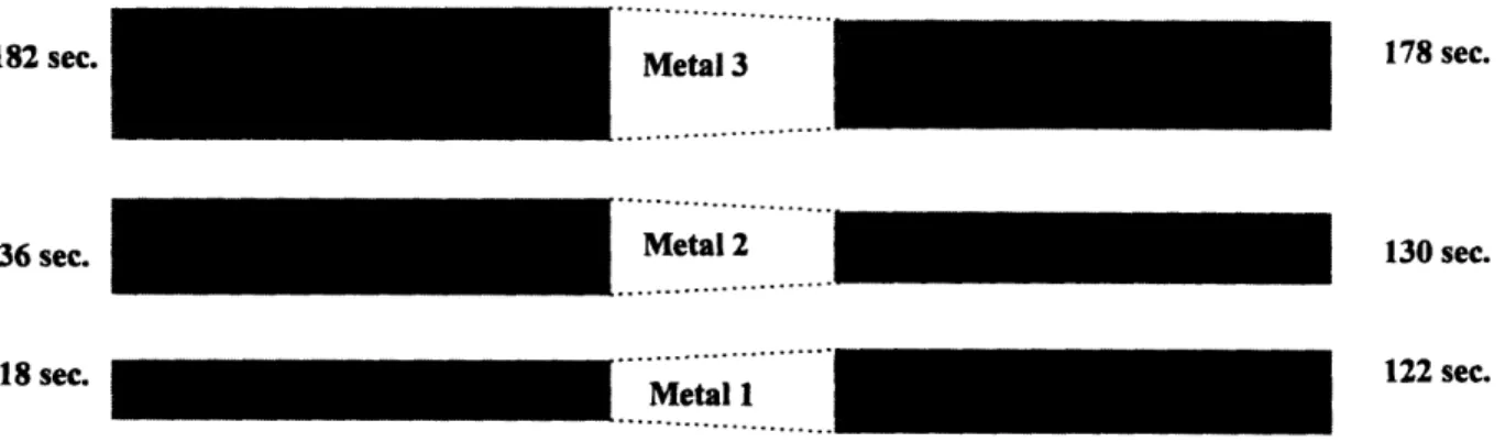
In the remainder of this paper a Metal 3 MQC refers to a check on Metal 3 and Metal 4 aluminum properties during a machine quality check.
4.2 Verifying Expected Performance of the Equipment
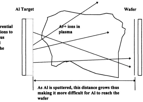
Sheet resistance, Rs, is used as a substitute check for the thickness of the aluminum being
deposited. It is used in place of a thickness check because the measurement is easier and less costly to perform. To make a thickness check, the MQC wafer is partially covered with a piece of tape and processed through an etch step. The metal underneath the tape is
left intact while the metal that is not covered is stripped away. Then, the height of the ledge from the top of the metal that was covered by the tape down to the MQC silicon surface is measured. This etch process is an extra step that takes considerable time to perform. This not only keeps the MDT from returning to operation, but it also uses valuable processing time at an etching tool. For Rs the MQC can go directly to the metrology tool thus reducing cycle time. Sheet resistance is a function of the resistivity
of the film being deposited and its thickness, where resistivity and thickness are measured in Ohms-cm and cm respectively. R, is a measure of Ohms per square such that a metal line can be divided into a total number of squares, then multiplied by Rs to give the resistance of the line.'l
Rs = p / T Where p = resistivity (Equation 4-1)
T = Thickness
Before beginning an analysis of the sheet resistance data itself, it is important to test that equation 4-1 holds true for the MDT machines (that is, to check that a consistent
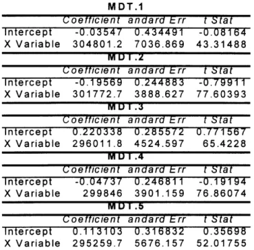
resistivity results from the deposition). Although not collected on a daily basis, thickness measurements and their corresponding sheet resistances are collected whenever a new aluminum target is installed in an MDT. Typically, this occurs whenever an old target has exceeded 575KWH of operation. This information is stored and available within a program called SPCView*. Using Microsoft Excel linear regressions were run for each
to Murarka, Shyam P., Metallization: Theory and Practice for VLSI and ULSI, Boston: Butterworth-Heinemann, p.41, 1993. SPCView is an internally developed program at Digital Semiconductor used to store and display information for Statistical Process Control purposes.
machine; R, as the independent value (y-value) and the inverse of thickness as the dependent value (x-value). The results of these regressions are included in the table below. Details of both the data and regression results are found in Appendix 1.
MDT.1
Coetficient andard brr t Stat
Intercept -0.03547 0.434491 -0.08164
X Variable 304801.2 7036.869 43.31488
M1I1 I .2
Coeftticient andard Err t Stat
Intercept -0.19569 0.244883 -0.79911
X Variable 301772.7 3888.627 77.60393
MUI .3
Coefficient andard -rr t Stat
Intercept 0.220338 0.285572 0.771567
X Variable 296011.8 4524.597 65.4228
M1UI .4
(oetticient andard E-rr t Stat
Intercept -0.04737 0.246811 -0.19194
X Variable 299846 3901.159 76.86074
M U . 5
Coefficient andard Lrr t Stat
Intercept 0.113103 0.316832 0.35698
X Variable 295259.7 5676.157 52.01755
Table 4-1: MDT Sheet Resistance vs. Thickness Regression Results
In all five cases the t-statistics provide strong evidence of the validity of Equation 4-1. In Table 4-1, the X Variable 1 stands for the slope or p-value of the regression equation, in this case an estimate of p (Equation 4-1). All five p estimates are within one standard deviation of the expected value of 300,000 kohms-angstrom (= 3.0 ohms-cm).
Additionally, the t-statistics for each intercept show that an intercept estimate or ca-value for each regression includes 0 within each regressions' 95% confidence intervals; thus the hypothesis that the intercept = 0 cannot be rejected.
These results indicate the machines are performing as expected and the sheet resistance measurements are a good measure of the thickness deposited by the machines. Because
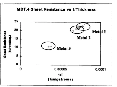
the data used to run these regressions is not normally distributed, confidence and prediction limits cannot be accurately calculated. There are clumps of localized data points due to the process being targeted at certain thicknesses for the different layers (Figure 4-2). This lack of normality in the data does not negate the effectiveness of the regressions. Using the residuals as an estimate of the natural process noise or e-value of the regression, a plotting of the residuals does show normality. These results are located in Appendix 1. Another important point to note here is that p can be treated as a constant value. It does not drift with time, it is the same across all aluminum film deposition processes (M -M3), and it does not vary between MDTs.
MDT.4 Sheet Resistance vs l/Thickness
25
20
Met 11
i 15 Metal 2 10 C Metal 3 0.= 5 0 0 0.00005 0.0001 1/T (1/angstrom s)Figure 4-2: MDT.4 Sheet Resistance vs. 1/Thickness Graph
4.3 Regression Analysis on Historical Data
As stated above, the sheet resistance MQCs are run in order to check that the MDTs are depositing the correct thickness of aluminum for each specified layer. Including checks for all different layer thicknesses implies that there is not a strong commonality between how the machine is being operated to sputter the different films. In reality this is not true.
The deposition of aluminum always occurs in the same chamber for a particular machine. The difference between layers is the combination of steps used to create the full stack of aluminum. Each layer is composed of several aluminum depositions; each deposition step lasts for a set period of time at a particular RF power. Although the arrangement of these steps is unique to each layer, the underlying physics of the sputtering process is not. Therefore, it is reasonable to suppose that by checking a single sheet resistance, one can have a strong indication as to the thicknesses of other layers without having to check them also.
The benefits of reducing MQCs are two-fold.
1. The availability of the machine to run product wafers rises. 2. Costs savings due to using fewer monitors can be achieved.
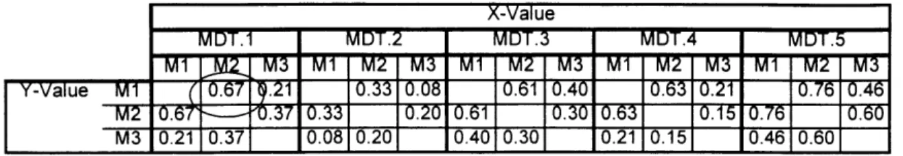
The first step to realizing some of these gains is to find clear numerical relationships between the sheet resistances of the various layers. Because the MQCs are run on a daily basis, there is a tremendous amount of data available. From this data linear regressions were run. In setting up the regressions, the sheet resistance values from one particular MQC were used as the dependent variable (x-value) and the values from another used as the independent (y-value). Included in Table 4-2 below are the R2 results of these
regressions. The circled value is the R2 result using a list of MDT. I's Metal 2 and Metal 1 sheet resistance values as the x and y variables respectively in a linear regression. R2 is used as indication of the proportional improvement a regression equation, as described by
y = ca + Px, makes over a horizontal line described by y=C, where C is the mean of the y
values used in the regression. It is often used as a measure of the "goodness of fit" of the regression line in capturing the relationship between the parameters for which the
regression was run. A value close to 1 means the regression describes the relationship well, while a value close to 0 does not.
MDT.1
0.21 0.37
X-Value
Table 4-2: R2 Results from Actual Sheet Resistance Regressions
Where R2 breaks down as a good indicator is when the relationship being regressed actually is constant. In the MDT case the supposition is that as sheet resistances rise for one metal layer, they will rise for the others. This means the slope of the regression will
not be equal to 0. Thus, using R2 as a first level indication in evaluating the regressions is
valid. Details of both the data and regression results can be found in Appendix 1. As can be seen from Table 4-2, the results are not very encouraging. The R2 values do not
suggest with confidence that the regression equations accurately capture the relationship between the sheet resistance of one metal layer based on another. This is a disturbing finding considering these MQCs are run through each MDT one right after another, suggesting changes in machine performance can take place very quickly between individual wafers.
4.4 Searching for Causes of Failure in Historical Data Regressions
Because the regressions for verifying equation 4-1 were so good, it is hard to believe there is a dramatic change in machine performance between individual wafers when machine performance does not appear to be changing dramatically over time and over different aluminum targets. Targets are changed roughly every two to three weeks. Therefore, an examination of other possible causes is needed. What became evident in looking at the data was an inconsistent setting of deposition times between the different metal layers over the life of a single target and over multiple targets.MDT.2 M1 M2 M3 0.33 0.08 0.33 0.20 0.08 0.20 MDT.3 M1 M2 M3 0.61 0.40 0.40 1 0.30 0.40 0.30 MDT.4 0.21 M2 M0.153 0.2110.151 MDT.5 M1 M2 M3 0.6 .46 0.46 0.60 Y-Value M1 -M3M3