Anomalous Phenomena and Spectral Tailoring in
Photonic Crystals
by
Michael Ghebrebrhan
OC"T
3
-rm rr 20 1~-LYiSubmitted to the Department of Physics
in partial fulfillment of the requirements for the degree of
Doctor of Philosophy
at the
MASSACHUSETTS INSTITUTE OF TECHNOLOGY
ARCHIVES
September 2010
@
Massachusetts Institute of Technology 2010. All rights reserved.
. n A
A uthor...
Certified by ...
Francis Wright
Department of Physics
August 15, 2010
... ...f..
..John D. Joannopoulos
Davis Professor of Physics
Thesis Supervisor
Z-/I
Accepted by...
...
-..-.
Krishna Rajagopal
Associate Department Head for Education
Anomalous Phenomena and Spectral Tailoring in Photonic
Crystals
by
Michael Ghebrebrhan
Submitted to the Department of Physics on August 15, 2010, in partial fulfillment of the
requirements for the degree of Doctor of Philosophy
Abstract
Photonic crystals are recently discovered meta-materials whose optical properties arise from periodic refractive index variations. In this thesis I examine various as-pects of photonic crystals including a self-assembled photonic crystal, anomalous properties arising from periodicity, and tailoring absorption and emission spectra. Fabricating photonic crystals with the desired properties in the infrared and optical frequencies, including a complete photonic bandgap, is an experimental challenge. Self-assembly can provide a solution. In Chapter 2, I examine a new type of colloidal photonic crystal of tetrahedral building blocks in a fcc lattice that is found to possess a robust and complete bandgap. In Chapter 3, I explore the photonic states that ex-ist around a zero-group velocity point. Motivated by negative refraction, a measure of the effective wavevector is constructed that distinguishes various types of zero-group velocity modes. Around one type of zero-zero-group velocity mode, an anomalous region of backward effective wavevector is found that enables superior light confining properties of a mirror-less cavity. In the last two chapters I look at the problem of efficiently converting radiant energy to electrical power. In Chapter 4, I explore the extent to which ID multi-layer thin films can enhance the short circuit current of a 2 pam-thick silicon solar cell. Though such cells are limited by their size, for two front-layers a relative boost of 45% is possible. Finally, in Chapter 5, motivated by the problem of low efficiency in thermophotovoltaics, I look at selective emissivity of a 2D metallic photonic crystal. A semi-analytical theory is developed using only the material dispersion and geometrical parameters. Applications of the selective emitter, including power generation and lighting, are discussed.
Thesis Supervisor: John D. Joannopoulos
Acknowledgments
This thesis would not be possible without the support and guidance of those around me. Over the years I spent here at MIT, I've been fortunate to gain much from people who've help me grow as a scientist and as a person. First I want to thank my advisor John Joannopoulos for his generous patience, guidance, and support during the course of my Ph.D. I was pretty lucky to work on photonics at this exciting time when there so many opportunities, and John is second to none when it comes to passing on this enthusiasm. I also wish to thank professors Steven Johnson and Marin Soljae'i6 for sharing their amazing physical insight. Finally I wish to thank my thesis committee, John, Marin, and professor David Litster, for taking the time to read this thesis and sit on the committee.
There are many within the JDJ/SGJ/MS group that took out time for me and shared their knowledge. My 12-111 officemates, Peter Bermel and David Chan, helped me get started with the different software our group used. Peter especially has always been willing to help- whether it was problems with Debian, the supercom-puters, or some physics question. Mihai Ibanescu's guidance during my early years cannot go unrecognized, sharing an interesting paper he found or taking time for my questions. My neighbors in the new CMT building, Aristos Karalis and Alejan-dro Rodriguez, always had time for enlightening discussion. Karen Lee was a great officemate to have. Ivan Celanovic, who worked closely with the group, made the selective emitter project fun. Finally to the rest of the group, I extend my thanks!
Outside of the JDJ group, Mark Rudner stands out. He is a great friend and amazing colleague, a combination not easily found. Mark keeps it real. The 8.333-8.511 homework group composed of Mark, Steve Jordan, Seungeun Oh, Pouyan Ghaemi, Rich Ott, and myself was a source of friendship since the very first week I
started here. Lastly the Black Graduate Students Association was always a source of camaraderie.
My time here was greatly enhanced by the community I found outside of MIT. A special thanks belongs to Habtom Ghiorgis for both his friendship and introducing me to the Eritrean community here. They have been like a second family. In particular, Musie Ghebremichael and Aman Russom have been like older brothers, who always had advice and served as sources of inspiration.
I've been most fortunate to have Rays Jiang in my life. Her presence, spirit, and intellect rejuvenates and inspires me.
Finally and most importantly, I wish to acknowledge the unending love and sup-port from my parents and sister, who've made this possible. I remember the very first science book my parents bought for me when I was a small child; I had no idea where it would eventually take me. The weekends and summers I spent working with my dad laid the foundation for everything I do now. A well-timed phone call from my parents would revitalize me and quickly erase doubts and frustrations. It is their love that drives me forward.
Contents
1 Introduction
1.1 The photonic crystal in detail . . . . 1.2 Thesis overview . . . .
2 Tetrastack: colloidal photonic crystal
2.1 Introduction . . . . 2.2 Tetrastack . . . . 2.3 Fabrication of tetrastack . . . . 3 Distinguishing zero-group velocity
3.1 Introduction . . . .
3.2 "7H in ID photonic crystals . .
3.3 'qH in 2D photonic crystals . .
3.4 Mirrorless cavity . . . .
4 Optimization of front coatings 4.1 Introduction . . . . 4.2 Formulation of the problem . . . 4.3 Results and discussion . . ....
modes in photonic crystals 35 35 38 40 46 54 54 56 62
4.4 Conclusions and future work . . . . 75
5 Tailoring thermal emission via Q-matching of photonic crystal res-onances 78 5.1 Introduction . . . . 78
5.2 Loss rates of waveguide resonances . . . . 80
5.3 Effect of period . . . . 84
5.4 Coupled-mode theory . . . . 88
5.5 Applications and conclusions . . . . 93
List of Figures
1-1 From left to right, one-, two-, and three-dimensional photonic crystals. Red and blue denote regions of low and high index. . . . . 16 1-2 Band structure of a three-dimensional photonic crystal. The photonic
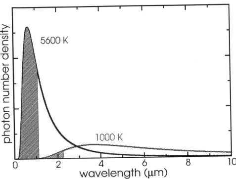
bandgap is highlighted yellow. . . . . 19 1-3 Photon number flux per unit wavelength of two blackbody emitters,
one at 5600 K (blue) and another at 1000 K (red). The spectrum of the cooler emitter has been rescaled by 100. Shaded regions denote useful photons for a silicon (blue) and InGaAsSb (red) PV diode. . . 22 2-1 (a) SEM images of fabricated tetrahedral colloidal particles. (b) Tetrastack
particles at the lattice points of the photonic crystal. (c) Conventional unit cell of diamond photonic crystal. . . . . 26 2-2 Band structure of inverted tetrastack in silicon
(nc
= 3.4) with sphereradius 0.27a. Inset, a portion of the tetrastack photonic crystal unit cell. . . . . 28 2-3 Bandgap map of ZnS-air (nc = 2.29) and Si-air (nc = 3.4) colloidal
structures. . . . . 31 2-4 Relative bandgap size versus index constrast for various structures at
2-5 Rotating the tetrastack particles away from the unit cell main diagonal (111) to a face diagonal (110) reduces the size of the bandgap. . . . . 33 3-1 Typical ID band structure for a Bragg mirror with high dielectric
E= 9 and width d = 0.2a . . . . 37 3-2 (a) 'qH calculated across the 1st and 2nd bands. (b) The magnitudes of
the dominant Fourier components across the second band of Fig. 3-1. Away from the band edges, where strong mixing occurs, the second
band behaves as a plane wave with ka/27r -+ ka/27r - 1. .. . . . . . 39
3-3 2D band structure with dielectric profile (inset) E = 9, r = 0.2a. Circled are the different types of zero-group velocity points; labels indicate location in the irreducible Brillouin zone and band number. 41 3-4 'H for the first four bands of the two-dimensional crystal in Fig. 3-3. 42
3-5 (a) k+G associated with the largest Fourier components for the second band, and magnitudes of associated Fourier components across the same band. (b) k + G for third band, and magnitudes of associated Fourier components across the band. . . . . 44 3-6 (a) Plot of q (thin lines) and (thick lines) for the second band. Color
indicates the field used as the weight: H (blue) and D (red). (b) Same comparison but for the third band where behavior is expected to be norm al. . . . . 45 3-7 Photonic-crystal Fabry-Perot cavity, formed by a finite number of
lay-ers of the crystal in the (11) direction. Here, the thickness is L = 12d, where d = a/V 2 is the distance from one row of rods to the next.
Blue/white/red indicate positive/zero/negative E2 field of a resonant m ode with
Q
~ 2000. . . . . 473-8 Resonant modes of a cavity formed from an finite section of a photonic crystal. The units of length is d = a/v 2 where a is the lattice constant. The dashed gray lines mark the induced periodicity due to the k point with zero-group velocity. For (a) ka/21r = (0.293, 0.293) at E2, (b) ka/27r = (0.5, 0.5) at M1 & M2 and (c) ka/27r = (0.318, 0.318) at E4. 49 3-9 The second band minimum is shifted to ka/27r = (0.33, 0.33), which
yields the same oscillatory dependence on L seen in the fourth band in F ig. 3-8(c). . . . . 50 3-10 Differences in the number of excited modes (circles) for the two cases
in Figs. 3-8(a) and 3-8(b). . . . . 52 4-1 Schematic illustration of solar cell designs studied here: (a) a
photo-voltaically active silicon region (green), backed by a perfectly reflecting metal (gray), (b) diagram (a) with one or more front coating depicted in shades of blue, and (c) diagram (b) with one back dielectric coating layer. . . . . 57 4-2 Fits of calculation parameters (red curves) to actual data derived from
references (blue curves): (a) real index of crystalline silicon
[1]
(b) absorption length of crystalline silicon [1] (c) current weights w(A) in Eq. (4.1), fit with a degree-100 Chebyshev approximation [2]. . . . . 59 4-3 A contour plot of the FOM of a cell with two front-coating layers versusthe layer thicknesses (the indices of each layer are fixed at 1.27 and 4.35). The FOM ranges from 0.30 (blue) to 0.38 (red). The presence of many local optima necessitates a global optimization approach. 60
4-4 The generated current efficiency as a function of wavelength; the pa-rameters for each structure class (e.g., two front layers) are optimized separately at each wavelength i.e., this is the reflection spectrum for many different structures. Note that structures with one or more front layers display full absorption up to a particular wavelength At that in-creases with the number of front layers. . . . . 63 4-5 The absorptive
Q
(magenta) and the radiativeQ
of 1,2, and 3 frontcoatings versus wavelength. Below 550 nm Q-matching is unnecessary, since the absorption length is equal to or less than the silicon layer thickness, and absorption is due to an anti-reflection coating. . . . . . 65 4-6 The generated current efficiency versus the bandwidth of incoming
radiation; for bandwidths up to 265 nm the central wavelength is 902.8 nm, for bandwidths above 265 nm, the maximum wavelength is fixed, while the minimum wavelength is decreased (which corresponds to a blue shift of the central wavelength). . . . . 68 4-7 Absorption spectrum over the full absorbing bandwidth for a
thin-film crystalline silicon solar cell (t = 2pLm). (a) Optimized over the full bandwidth and (b) optimized only at A = 902.8 nm. . . . . 69 4-8 Figure of merit versus silicon slab thickness, both for a structure with
no front layer (based on Fig. 4-1(a)) and optimized structures with 1-3 front layers (based on Fig. 4-1(b)). . . . . 71 4-9 Relative difference in figure of merit, calculated as the relative
differ-ence of the FOM for the optimized structure with the given reflection phase and the FOM of a structure with the given phase and with the optimized front coating of the reference phase (0 = 0), versus the
4-10 Absorption spectrum of the optimized single front coating reference structure for two different back-reflector phases, -r/4 (blue) and -r (red). The back-reflector simply shifts the peaks, but has a only neg-ligible effect on the integrated absorption or the FOM. . . . . 74 5-1 Emissivity spectrum of flat, bulk tungsten (blue) and of an ideal
se-lective emitter (green) designed to match the 0.6 eV/h bandgap of InG aA s. . . . . 80 5-2 A periodic array of cylindrical holes with period a, depth d, and radius
R etched into a slab of tungsten. The hole depth is less than the
tungsten slab thickness. . . . . 81 5-3 (a) Resonant mode frequency in units of 27rc/a with a = 1 pim, (b)
Qabs,
and (c) Qrad of the lowest three modes. The absorptive andradiative
Q
are plotted on the same color scale. Q-matching of the first resonance is indicated by the white line. . . . . 835-4 Qrad versus period of unit cell with R = 0.545pm and d = 1.89pm.
Resonance with a diffracted plane wave sets up an anti-crossing, visible as large jumps in Qrad. Since we consider resonances that couple only to normal incidence, the period is bounded from above. . . . . 85 5-5 Absorption spectrum for the tungsten photonic crystal slab with a =
4.8pm, R = 0.104a, and d = 0.394a. Diffraction appears as sharp peaks and weak resonant peaks due to photonic crystal modes appear at approximately 2.7 and 3.4 2rc/a. . . . . 87 5-6 Absorption spectra for photonic crystal slabs with various a but R
5-7 A multimode resonator with resonant frequencies w, absorptive and radiative lifetimes Tabs,i and Trad,i, respectively. Resonances i and
j
radiatively couple to each other with rate 1/rij. . . . . 90 5-8 Absorptivity spectrum for a = 1.2 pm calculated by FDTD simulation
List of Tables
2.1 Table of gap-midgap percents for fcc, diamond, and tetrastack pho-tonic crystals. . . . . 30 4.1 Table of optimized coating designs for one, two, and three
front-coating layers, as in Fig. 4-1(b). Layers are ordered from closest to air. Coating thickness d in units of nm. . . . . 68
Chapter 1
Introduction
Photonic crystals are media that interact with light via a wavelength-scale periodic refractive index modulation [3, 4, 5], illustrated in Fig. 1-1. This opens exciting pos-sibilities in the manipulation of light including negative refraction [6, 7], invisibility cloaks [8, 9, 10], and all-optical computing [11]. The information age we live in today was born from the understanding of the electronic properties of semiconductor crys-tals. One can imagine similar control over light would open the possibility of new technological breakthroughs just as solid state in the past. In this thesis I will dis-cuss the search for an easily fabricated photonic crystal with a full three-dimensional bandgap, the novel properties of states around certain zero-group velocity modes, and how photonic crystals can be used to modify both the absorptivity and emissiv-ity spectra of material systems. It is of interest to note that while we have recently discovered photonic bandgap materials, nature has been utilizing them for eons, vis-ible in the iridescence of butterfly wings [12, 13] beetle scales
[14],
and sea worms antenna [15].Figure 1-1: From left to right, one-, two-, and three-dimensional photonic crystals. Red and blue denote regions of low and high index.
1.1
The photonic crystal in detail
Since photonic crystals are periodic media, an analogy with semiconductor crystals can help us understand their signature property: the photonic bandgap. In a semi-conductor an electron sits in the periodic potential of the positive ions. Quantum mechanics tells us the electron is a wave, and the electron wave experiences multiple coherent scatterings that can constructively interfere in certain directions allowing it to propagate undeflected
1161.
For a certain range of electron energy values com-plete destructive interference occurs and there can be no propagating solutions to Schrodinger's equation; an electronic bandgap is said to open up in this range of energy values. Similarly, in a photonic crystal an electromagnetic wave experiences a multiple coherent scatterings due to the periodic index modulation and can propa-gate in certain directions undeflected. There may also exist certain frequencies that do not correspond to a propagating solution. This band of frequencies is called the photonic bandgap. In other words, a normally transparent material can be made in a mirror! Moreover, just as doping a semiconductor crystal with atomic impurities whose energy lies within the electronic bandgap of the host can create spatially local-ized states, engineering a defect in a photonic crystal can create a spatially locallocal-izedelectromagnetic state [5]. This is only the beginning of the kind of control we can achieve.
Let us dig in a little deeper; by assuming a harmonic time-dependence and rewrit-ing Maxwell's equation as a Hermitian eigenvalue problem we obtain a Hamiltonian for the photon,
1
w2
Vx VxH=-H (1.1)
E(r) C2
where H is the magnetic field, E(r) describes the dielectric, W the angular frequency, and c the speed of light. Due to the periodic boundary conditions, the solutions to Eq. 1.1 appear as bands giving rise to the photonic bandgaps. The states adjacent to a bandgap display qualitative difference; those that are below store most of the electric field energy in the high dielectric region and those above the bandgap store most of there electric field energy in the lower dielectric region. New opportunities open up with the band gaps- sub-wavelength confinement and guiding of light[5, 3, 4, 17], slow light[18, 19, 20], and omni-directional reflection [21, 22]. For crystals with a bandgap, the termination of the crystal can allow solutions that are localized on the surface. (Such surface states are the subject of Chapter 5.)
Since a photonic crystal possesses periodic translational invariance, a crystal wavevector can be associated for each solution,
Hk(r) = eik'rhk(r), (1.2)
where k is the Bloch wavevector and hk is a periodic function. Because there is only periodic translational invariance, the unique set Bloch wavevectors live within a unit cell of k-space, the Brillouin zone. The set of all solutions to Eq. 1.1 can be expressed as a relation between the frequency and wavevector, the band structure.
However, symmetries of the real space lattice can be exploited to drastically reduce the number of points in reciprocal space needed to find bandgaps. Once this reduction of the Brillouin zone is accomplished, the frequencies of the allowed solutions can be plotted versus the crystal wavevector along the high symmetry planes of the irreducible Brillouin zone, Fig. 1-2. Unlike a homogeneous medium with ellipsoidal equifrequency surfaces, photonic crystals possess more complex dispersion relations and equifrequency surfaces. Moreover, the gradient of the equifrequency surface gives the group velocity,
Vg = VkW(k). (1.3)
This opens the way for novel properties such super-collimation [23], all-angle negative refraction [7], and spinning photonic states [24]. A complete understand these novel properties will allow us to use them to enable new behaviors of older technologies.
While there are many similarities with the electronic case, differences arise. One key difference from the electronic case is the photonic Hamiltonian and it's solutions are scale invariant, solutions at one frequency may be scaled up or down simply by scaling the geometry appropriately. This flexibility allows the researcher to place these bandgaps at any frequency they choose provided that all lengths are scaled accordingly and the same epsilon values can be found at those frequencies.
1.2
Thesis overview
Here, I give a brief overview of the contents of the chapters, motivating each chapter and highlighting key results. In Chapter 2 I describe a realizable colloidal photonic crystal, "tetrastack", composed of tetrahedron-shaped particles that possesses a ro-bust, complete bandgap even for small index contrasts [25]. Next in Chapter 3 I
0.5
0.3-Figure 1-2: Band structure of a three-dimensional photonic crystal. The photonic bandgap is highlighted yellow.
show using a quantity that measures the angle between the group velocity and av-eraged wavevector that there exists states around certain zero-group velocity points where the angle is obtuse
[26].
A physical manifestation of this unusual character is given. In Chapter 4 the optimal benefit of thin front coatings on thin silicon is determined and found to be over 50% even forjust
two front coatings[27].
Finally in Chapter 5 I show how with a few geometrical parameters, the emissivity spectra of metals can be tailored at will with photonic crystals, opening the way for higher efficiency thermophotovoltaic systems[28].
Though there has been much theoretical and computational advance since 1987, fabrication of photonic crystals is still laborious. Cheap, scalable fabrication of pho-tonic crystals with a full three-dimensional band gap has remained elusive. The techniques that work well for one- and two-dimensional crystals, thin film
deposi-tion techniques such as physical and chemical vapor deposideposi-tion, and molecular beam epitaxy, and photolithography and etching, require much effort for building three-dimensional crystals. An attractive alternative presents itself in self-assembly.
Self-assembly is an attractive route for building three-dimensional crystals since uniform building blocks can be made in large quantities and can be arranged into a crystalline pattern by allowing the particles to settle with minimal direct guid-ance. This process is good enough for nature to take advantage of it- opals are self-assembled photonic crystals of silica spheres with lattice constants on the order of 100 nm, giving rise to diffraction in the visible range. However, monodispersed spheres tend to settle into a closed-packed face-centered cubic structure which does not't have a bandgap for any value of index contrast[5}. Moreover a diamond-like structure, which possesses a robust bandgap, is not a thermodynamically favored structure and will not form via self-assembly. In Chapter 2 of this thesis I show that crystals made of non-spherical particles allow a bandgap to open. The most promis-ing of these non-spherical particles is "tetrastack", a particle with four fused spheres in a tetrahedron. Moreover due to the control over the sphere size and amount of fusion one could create the bandgap over a wide range of frequencies. A group theo-retic explanation for the properties of a tetrastack crystal is given, and the effect of orientational disorder is explored.
In the third chapter I identify and explore certain anomalous regions in the band structure in two-dimensional photonic crystals. In nature we find that homogeneous media have positive index, and the group velocity and phase velocity (or equivalently the wavevector) of light travelling in these media are parallel to one another. In neg-ative index media, recently realized in certain meta-materials
[29],
the group velocity and phase velocity point in exactly opposite directions allowing light to do unusual things including negative refraction, superlensing, and anomalous Cerenkov radiation[30, 31]. Periodic media such as photonic crystals possess band structures that at first sight appear to have modes with opposite group velocity and wavevector. However the wavevector is a crystal wavevector which does not correspond to a phase velocity and can be made to point in any direction by adding a reciprocal lattice vector. For one-dimensional crystals we will see that a mode with negative group velocity and positive wavevector is actually one with negative effective wavevector. In higher dimensional crystals, however, it may be possible to find modes with group velocity and effective wavevector making an obtuse angle with each other. Such modes have never before been identified in positive effective index media. In Chapter 3 I will define a measure of the effective wavevector and show that indeed there are certain regions in the band structure where the angle it makes with the group velocity is obtuse. These novel regions are associated with a particular type of zero-group ve-locity mode. In addition, we will see that around those special zero-group veve-locity modes it is possible to make mirrorless cavities of unusually high quality factors.
The last two chapters conclude with shaping the spectral response of materials to boost the efficiency of photovoltaic cells. A thermal source of photons, such as the Sun, illuminates a photovoltaic diode that converts a portion of the incoming energy to electrical power. However without modifying the absorptivity of the PV diode or the emissivity of the source, much of the energy is lost through reflection or delete-rious heating. In the case of a silicon solar cell, much effort has gone into decreasing the losses to such an extent that efficiencies for thick silicon solar cells approach the fundamental limit set by detailed balance and silicon's material properties [32, 33]. However, thick, crystalline silicon is expensive and the use of thin (about 1 pm), crystalline or micro-crystalline silicon is becoming increasingly cost-competitive. In Chapter 4, I consider what improvements in efficiency can be made with multiple, thin front and back coatings on a thin silicon cell. Unlike thick silicon cells where
0 2 4 6 8 10
wavelength (gm)
Figure 1-3: Photon number flux per unit wavelength of two blackbody emitters, one at 5600 K (blue) and another at 1000 K (red). The spectrum of the cooler emitter has been rescaled by 100. Shaded regions denote useful photons for a silicon (blue) and InGaAsSb (red) PV diode.
any transmitted light is absorbed, thin silicon cells present the possibility of inter-ference of reflections from the back surface since a single pass is not always enough to absorb a photon. This presents an unexplored challenge. I show that significant improvements, a nearly 50% relative increase in efficiency over an uncoated cell, can be made with simply two front coatings. Moreover, while one could imagine using many more front coatings, we will see that the majority of the improvements come from just the first few layers.
For a thermal source of photons, such as a blackbody, whose spectral distribution is given by the Planck distribution, a significant amount of power is radiated at frequencies in the infrared, below the bandgaps of most semiconductors, illustrated
in Fig. 1-3. For thermophotovoltaic schemes which use a radiator at temperatures much lower than 5600 K, this is disastrous. Consider a typical power generator using a radiator at 1000 K and indium gallium arsenic antimony (InGaAsSb) as the PV diode; the ratio of useful power to total radiated power is less than 19%. However, by modifying the surface of the radiator, it is possible to tailor its emissivity spectrum to closely match the quantum efficiency of the PV diode.
In Chapter 5 of the thesis I examine a particular type of selective emitter, a two-dimensional array of holes etched onto a metal, and how one could tailor its emissivity spectrum. Though the simplest approach would be to use multiple one-dimensional front coatings, a two-one-dimensional periodic array of holes offers greater benefits. Moreover the use of multiple materials is problematic since all of them must be thermal stable and non-absorptive at high temperatures. Using a one-dimensional periodicity is not enough since not all polarizations and directions are treated the same. For thermophotovoltaic applications, one would like a thermal emitter with minimal emissivity in the infrared and a high melting point. Refractory metals, including tungsten, satisfy both requirements. The hole array creates photonic res-onances, solutions to Eq. 1.1 with a complex frequency, that are localized to the surface. The key to the selective emissivity is that the resonances exist only above a cutoff frequency that is determined by the geometrical parameters. In addition, the geometrical parameters determine how strongly these resonances radiate. I look at how one can analytically predict where these photonic crystal resonances exist and their lifetimes, which allow one to compute the emissivity spectrum via a scatter-ing matrix framework, i.e., temporal coupled-mode theory. To study this problem more efficiently the absorption spectrum is calculated- Kirchhoff's law states that the absorptivity and emissivity are the same for an object in thermal equilibrium. While computational methods for computing the absorptivity spectrum, such as
finite-difference time domain or finite-element methods, yield accurate results, they are computationally intensive. Once one can semi-analytically compute the absorp-tivity spectrum, then optimization of the spectrum for thermophotovoltaic systems and other applications becomes possible.
Chapter 2
Tetrastack: colloidal photonic
crystal
Photonic crystals strongly localize photons of certain frequency, offering a novel means to control light
[5].
This control over light is achieved via the periodic refrac-tive index modulation of the photonic crystal which allows a photonic bandgap to open in a manner analogous to the electronic bandgap of a semiconductor crystal. While photonic crystals are expected to enable the production of high performance optoelectronic devices- lossless waveguides[34],
photocatalysts based on extended lifetimes of excited species[35],
low threshold, highly efficient semiconductor lasers [36], and nonlinear optical switches [37]- few structures have been found that possess the complete 3D photonic band gap required for the promised degree of light control. Here one possible solution based on a colloidal photonic crystal is described. The building block are colloidal tetrahedra arranged in a fcc lattice. A robust omnidirec-tional bandgap is found and compared to diamond.(a) (b) (c)
Figure 2-1: (a) SEM images of fabricated tetrahedral colloidal particles. (b) Tetrastack particles at the lattice points of the photonic crystal. (c) Conventional unit cell of diamond photonic crystal.
2.1
Introduction
Three-dimensional (3D) periodic structures have been successful made at the micron length scales corresponding to bandgaps in the infrared [38], however it remains a challenge to easily fabricate photonic crystals at the submicron length scale necessary for devices operating within the visible and near-infrared region. Producing such photonic crystals requires the fabrication of lattice elements with a feature size of a few hundred nanometers. Relative to 3D lithography approaches
[39,
38], colloid-based solutions for the fabrication challenge are highly attractive due to the ease of accessing the submicron size regime and relative low cost for the buildup of 3D structures. Colloidal photonic crystals have been fabricated with a periodicity of about 170nm which display a partial photonic band gap in the violet-ultraviolet, a feat not yet duplicated with lithographic based photonic crystals [40].Self-assembly of monodispersed spheres leads to energetically favorable structures with high packing density which includes face-centered cubic (fcc). The fcc structure,
however, has no bandgap irregardless of the refractive index contrast nc between the spheres and the surrounding medium due to degeneracy at the W k-point. On the other hand, the inverted fcc structure, a lattice of air spheres in a high index medium, i.e., inverse opal, can possess a bandgap between the 8th and 9th bands for a refractive index constrast of at least 2.9 [41, 42]. The utility of higher order bandgaps is lessened since such bandgaps are sensitive to all types of geometric disorder including variations in the radii of the spheres and random displacements from lattice sites. Small amounts of disorder in the lattice constant amounting to a few percent can completely destroy the bandgap. Lower lying photonic band gaps, such as the one in diamond, are much more robust to disorder.
2.2
Tetrastack
Wide and robust photonic bandgaps between the second and third bands open for the diamond and inverted diamond crystal structures with relatively low index contrasts
[43]. However neither are thermodynamically favorable colloidal structures and do not form naturally. Recently, a pick-and-place nanorobotic method of building a col-loidal diamond structure was demonstrated; however the crystal was composed of just 165 silica spheres each taking an average of 3.8 minutes to place [44]. Alternatively, non-close-packed structures with diamond-like connectivity could be realized using colloidal cluster building blocks, with the "openness" of the final crystal structure and the mechanical stability provided by the geometry of their packing. Nonspher-ical colloids also offer reduced symmetry at the lattice point, a feature thought to promote the large stable band gap in the diamond structure [43]. Knowledge of the photonic properties of crystal structures based on colloidal cluster building blocks is limited, since only the diamond-like dimer structure has been explored in modeling
0.6-
0.4--0 S0.2
--U
L
F
X
W
K
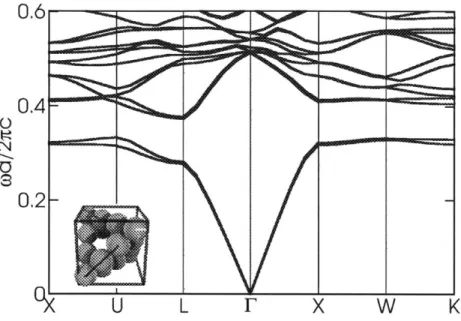
Figure 2-2: Band structure of inverted tetrastack in silicon (n, = 3.4) with sphere radius 0.27a. Inset, a portion of the tetrastack photonic crystal unit cell.
studies of the photonic bands 144, 451. The present theoretical study reports robust photonic bandgaps for a diamond-inspired crystal structure with a nonspherical, col-loidal tetrahedron basis. The plane wave expansion method with more than 4000 plane waves (corresponding to a resolution of 16 pixels per a) was used to calculate photonic band structures for the newly proposed "tetrastack" by solving Maxwell's equations in the frequency domain
[461.
The minimum refractive index contrast to open at least a 1% complete 3D-photonic band gap in the inverted tetrastack structure was found to be 1.94, making this one of the lowest threshold refractive index-contrast photonic crystal structures discovered. A more relaxed requirement for the refractive index contrast enlarges the range of materials appropriate for fab-ricating structures with omnidirectional photonic band gaps [47].The tetrastack photonic crystal structure is composed of tetrahedral colloidal clusters stacked to connect nearest neighbor sites in the fcc lattice where each sphere of a tetrahedron connects to a neighboring site. Figure 2-1(a) and Fig. 2-1(b) depicts the tetrastack structure in comparison with the diamond structure Fig. 2-1(c). The real-space structure is described as an fcc lattice with lattice vectors R1 = a/2 (y+i),
R2= a/2 (R + i), R3 = a/2 (R +
y),
where a is the length of the conventional cubiccell. The tetrahedron spheres are at positions, 0, R1/2, R2/2, and R3/2. One threefold symmetry axis of each tetrahedron points along the main diagonal of the fcc lattice, reducing the symmetry group of each lattice point from Oh (full octahedral group) to Td (tetrahedral group). Figure 2-2 shows the band structure calculated for the inverted tetrastack structure of air tetrahedra in a silicon matrix. As in the case of the diamond structure, the degeneracy between the second and third photonic bands at the W point for the fcc lattice is replace with a degeneracy in the first and second bands and a degeneracy in the third and fourth bands
[45].
Therefore a sizable bandgap can open for the appropriate combinations of refractive index contrast and solid volume filling fractionf.
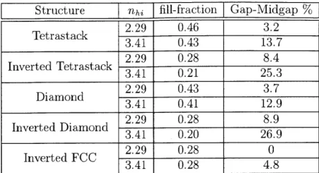
Table 2.1 compares the relative bandgap width AW/Weenter of tetrastack structures with those of the diamond and fcc structures and their inverted counterparts. Refrac-tive index contrast values for zinc sulfide-air (n, = 2.29) and silicon-air (ne = 3.41) were used in the calculations for both direct and inverted structures. Solid volume filling fractions that maximized the band gap for each structure were selected. Com-parable bandgap widths were found for inverted tetrastack and inverted diamond structures, 25.3% and 26.9%, respectively. The bandgaps were much larger than those for the corresponding inverted fcc structures at the same index contrast.
A wide range of solid volume filling fractions were found to exhibit full photonic bandgaps for tetrastack structures, as shown by the band gap maps in Fig. 2-3 for
Structure nah [fill-fraction Gap-Midgap % 2.29 0.46 3.2 Tetrastack 3.41 0.43 13.7 Inverted Tetrastack 2.29 0.28 8.4 3.41 0.21 25.3 2.29 0.43 3.7 Diamond 3.41 0.41 12.9 2.29 0.28 8.9 Inverted Diamond 3.41 0.20 26.9 Inverted FCC 2.29 0.28 0 3.41 0.28 4.8
Table 2.1: Table of gap-midgap percents for fcc, diamond, and tetrastack photonic crystals.
ZnS-air and Si-air materials. Constituent spheres touch at a solid volume filling fraction of 0.37 for direct tetrastack and 0.34 for direct diamond. Five distinct regions corresponding to structures of the same refractive index contrast, symmetry group, and connectivity of solid material can be identified in Fig. 2-3. The variety of structures represented by the area of the gap map is nearly as broad for tetrastack structures as for diamond structures. In particular, inverted structures of the same index contrast display wider bandgaps than their direct counterparts.
The effect of refractive index contrast on relative bandgap size near the solid volume filling fractions that optimize the bandgap for each structure is presented in Fig. 2-4. The bandgaps naturally fall into three groups corresponding to the connectivity of the high index region. The threshold refractive index contrast needed to create a full photonic bandgap is nc = 2.1 for direct tetrastack with
f
= 0.42 and nc = 1.94 for an inverted tetrastack withf
= 0.30. This is one of the few predictions of a full photonic bandgap in the case of a structure with a refractive index contrast lower than 2. Large bandgaps of 10% or more can be obtained at index contrasts0.7
0.6-Iniverted diamo nd, n=2.2930.4-invertdttatce
,0.3,-
inverted diamon r-3 4 0.-0
0.1
0.2
0.3
0.4
0.5
0.6
0.7
Fill Ratio
Figure 2-3: Bandgap map of ZnS-air (ne = 2.29) and Si-air (nc = 3.4) colloidal structures.
that are insufficient to open a bandgap in the inverted fcc structure of air spheres. For the structure composed of a colloidal dimer basis made from silicon, Li, Wang, and Gu [48] determined a relative bandgap width of 15.5% relative to the center frequency when the major axis of the dimer was oriented along the (111) direction and the solid volume filling fraction was 0.34. Note that for these parameters the dimer structure is equivalent to diamond. The bandgap was reduced to half its maximum value for a deviation angle of 50 from the main diagonal. In a similar manner the dependence of the photonic band structure on the tetrahedra orientation in the tetrastack structure was studied by calculating the relative bandgap width as the symmetry axis of the tetrahedra rotates from the (111) direction toward the (100) and (110) directions. Similar to the case of the diamond-analog dimer structure, the bandgap is maximized when the axes of the tetrahedra are oriented along the (111)
25
20-nverted tetrastacik, f=030 - inverted diamond, f=0.4715 -
1:'2 -diamrond-E
-=0
10 ---05-01
01
1.5
2
2.5
3
3.5
4
nlhiFigure 2-4: Relative bandgap size versus index constrast for various structures at filling fractions corresponding to optimal relative bandgaps.
direction, Fig. 2-5. The bandgap persists for the inverted tetrastack up to an angle about halfway between the main diagonal and a face diagonal. The bandgap width decreases to half of its original value for the ZnS-air system at a deviation angle
of 110 - 12' for inverted tetrastack and 5' - 6' for direct tetrastack. Thus a less
severe design requirement is predicted for orientation of the tetrahedra in inverted tetrastack than for dimers in the diamond-analog structure.
2.3
Fabrication of tetrastack
Up to 1010 colloidal cluster building blocks have been prepared using an emulsion trapping method [49] or a microfluidic confinement cell where specific configurations were determined uniquely by the particle diameter relative to the dimensions of
46--C
O
tetrastack, f=0.42
0
5
10
15
20
Angle of Deviation from (111) to (110)
Figure 2-5: Rotating the tetrastack particles away from the unit cell main diagonal (111) to a face diagonal (110) reduces the size of the bandgap.
lithographically defined holes [45, 50]. Similarly, Hammond and Lee 151] utilized a patterned template of positively charged polyelectrolyte dots to capture beads from a suspension of negatively charged carboxylated polystyrene and to create specific configurations of clusters determined by the bead diameter and the pattern dimen-sions. The clusters would be useful for nonspherical bases in inverted structures, but would not be appropriate for direct structures with a complete bandgap due to the low refractive index of the polystyrene building block, n = 1.6 [52].
An alternative method is to use tetrahedral clusters made through the controlled coalescence of high-index building blocks during their chemical synthesis as demon-strated for ZnS by Liddell [53]. Zinc sulfide spheres ranging from 0.5 to 2pm in diameter were clustered into dimers, trimers, and tetrahedra Fig. 2-1(a) using the
decomposition of thioacetamide at elevated temperatures in the presence of the metal salt. The ZnS particles exhibited a refractive index of 2.09 -2.25 in the visible region
[54}.
While optical tweezers could be used to prepare ordered structures from the building blocks [48}, directed assembly in electric, magnetic, and hydrodynamic fields [55] may be less laborious. A possible route toward fabricating a tetrastack colloidal crystal would be via a layer-by-layer convective assembly of tetrastack particles onto a compliment polyelectrolyte dot pattern [51]. A sacrificial film is then deposited onto the first layer of tetrastack particles to prevent the next layer from settling into the interstitial spaces between the first layer of tetrastack particles. Finally the poly-electrolyte pattern could be restamped to repeat the process until the target number of layers is achieved.In conclusion, a new experimentally attainable colloidal photonic crystal with a full and robust photonic bandgap has been described. Moreover for a range of refractive index contrasts, filling fraction, and tetrahedron orientation a bandgap will remain. Thus photonic crystals made from colloidal structures have the ability to substantially widen the range of realizable full 3D bandgaps.
Chapter 3
Distinguishing zero-group velocity
modes in photonic crystals
3.1
Introduction
Propagation of light in photonic crystals can be quite different from that in homoge-neous media, such differences include photonic band gaps, supercollimation, super-prism effects
[23],
and extraordinary or negative refraction[7].
Most of these effects are closely associated with an unusual feature of the dispersion relation (band struc-ture), the frequency w versus wavevector k, of periodic systems: there are extrema, or points of zero group velocity VkW. Such points do not occur in a homogeneous medium, only in localized modes of certain waveguide structures or in non-localized modes of periodic media. Since extrema in the frequency bands are so central to the unique phenomena possible in photonic crystals, we wish to investigate them more closely, and to ask the question: are there significant qualitative differences between different band extrema, and what relationship do these differences have to variousphysical phenomena? Naturally, there are some obvious qualitative differences: some extrema are maxima, some are minima, and others are saddle points. And, of course, the exact eigenmode solutions in the vicinity of the extrema provide, in principle, complete information about their behavior. But the latter is too much information-we would hope to have a simpler description of the differences betinformation-ween extrema than the entire field patterns-and the former is too little, as we shall see. In particular, we will argue that there are substantial differences between extrema at high-symmetry k points (such as the center or edge of the Brillouin zone, corresponding to the tradi-tional criteria for Bragg diffraction) and extrema at other k. And, even among these non-symmetric extrema, there are distinct differences between those arising from avoided eigenvalue crossings (anti-crossings) and other band-repulsion phenomena. As we will show these differences arise from general properties of periodic crystals, therefore such differences in zero-group-velocity should be found in other periodic systems, including electronic and phononic crystals.
In order to have a quantitative measure of these differences independent of any particular physical phenomena, we consider by analogy an important quantity of homogeneous media that is ill-defined in periodic structures: the phase velocity v, = wk/|k 2. In a homogeneous medium, the relative direction of the phase and group velocities reveals important information such as whether the medium is right-or left-handed (negative index) [30] and to what degree the medium is isotropic. In a periodic medium, the phase velocity is ill-defined because k is not unique-it is equivalent to k+G for any reciprocal lattice vector G [5]. Equivalently, an eigenmode in a periodic structure corresponds to an infinite number of Fourier components k+G, given by the Fourier-series expansion of the Bloch envelope, each with its own "phase velocity". However, we can use the amplitudes of these Fourier components, Hk+G,
1.5
1.25-2. 0. 75
--0.5
0.25
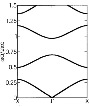
Figure 3-1: Typical ID band structure for a Bragg mirror with high dielectric e = 9
and width d = 0.2a
and the degree to which the "average" phase velocity is parallel to the group velocity, and we find that this average exhibits interesting distinctions between different band extrema. In particular, we define
G vg| _k+G|I Hk+G12
'qH = gHk±G12 - (3.1)
EG | Hk+G |
as a measure of the anomalous character of a mode. qH is bounded between -1 and 1, since it is a sum of cosines of the angle between the group velocity and the wavevector weighted by the Fourier component amplitude. A positive (negative) sign indicates normal (anomalous) character; in fact in the homogeneous, right-handed medium limit 'H is 1 for all modes. The form of this function is somewhat arbitrary, e.g. one
see later, alternative definitions of q yield similar qualitative results.
This difference has a physical consequence; as we'll see shortly the difference zero-group velocity modes give rise to very different light confinement behavior. This behavior is connected to the information presented in
7H-3.2
r/H in
1D
photonic crystals
Consider first a one-dimensional photonic crystal, such as a multilayer film of period a with alternating E = 9 (thickness 0.2a) and = 1 (thickness 0.8a), whose band structure w(k) (solved using a planewave method
[46])
is shown in Fig. 3-1. In such a structure, there are bands that have opposite-signed group velocity and k and which therefore appear "anomalous," but examining 7H, plotted in Fig. 3-2(a), reveals that they are not. The first band is clearly positive throughout the Brillouin zone. Moreover, it is the only band in which 'JH approaches a constant non-zero value as k vanishes, behavior due to the fact that vg approaches a constant non-zero value at low frequencies. The second band, which looks anomalous since vg is opposite tok in the first Brillouin zone, is shown to be "normal" in the sense of 7H: most Of
its Fourier components actually lie at negative wavevectors, aligned with vg. Since all other bands have the behavior of one of these two bands, it appears that all one-dimensional modes have similar, normal character.
Fourier decomposing the modes of the second band shows the lack of any anoma-lous character more explicitly. In Fig 3-2(b) the various Fourier components of the second band are plotted. The Fourier component Ga/21r = -1 is over 60% for most of the Bloch modes between ka/2r = 0 and 0.5. Effectively the mode at k behaves like a plane wave with k = k - 2wr/a. So the group velocity and "average" k point in the same direction. For vanishing k, the modes begin to have an additional mirror
kxa/21c
(a)0.8
-0. 6
--0.4-
0
0.2-
-200
0.5
ka/2x
(b)Figure 3-2: (a) r/H calculated across the 1st and 2nd bands. (b) The magnitudes of the dominant Fourier components across the second band of Fig. 3-1. Away from the band edges, where strong mixing occurs, the second band behaves as a plane wave
symmetry plane, so for every G there is a -G component that cancels its contribution
to IIH ensuring that YH goes to zero.
There is a simple argument why one-dimensional photonic crystals should not exhibit sign changes of YH, and therefore should not exhibit negative 9H for right-handed materials. To begin with, for a given frequency w, the allowed wavevectors k in a one-dimensional crystal come from the eigenvalues exp(ika) of a 2 x 2 transfer matrix [56], and thus there can be at most two distinct real-k solutions at each w.
This precludes the possibility of having more than two extrema in a given band, and by symmetry (either mirror symmetry or time-reversal symmetry) these two extrema must occur at the Brillouin-zone edges. By the same symmetry, however,
'7H cannot change sign at these points. The only remaining possibility would be for
"7H to change sign at a point that is not an extremum, where vg does not change
sign, but this seems unlikely and we have been unable to find such a circumstance.
3.3
7H
in 2D photonic crystals
For two-dimensional periodic structures there can be zero-group-velocity modes away from the Brillouin-zone edge or center. For example, a square lattice (period a) of dielectric rods (e = 9 and radius r = 0.2a) in air illustrates this new type of zero-group-velocity mode at k = E where E lies on FM, (Fig. 3-3), which itself can be divided into further subcategories. Around the M-point, repulsion occurs between the second and fourth bands that causes the second band to develop a local minimum, where we might hope to find unusual behavior compared to a homogeneous right-handed medium. The repulsion that drives the second band downward originates in the shared symmetry character of the second and fourth bands under reflection about the mirror plane that contains k along FM. Perturbative analysis of the modes
S0 . 4 .. 4M Y-2
0.4-
-i
0.2--S' E
M
X
l'
Figure 3-3: 2D band structure with dielectric profile (inset) e = 9, r = 0.2a. Circled are the different types of zero-group velocity points; labels indicate location in the irreducible Brillouin zone and band number.
0.8 -
band 1I0.8-0
-0.2
2 -0.2 band 2 l' T. MFigure 3-4: qH for the first four bands of the two-dimensional crystal in Fig. 3-3.
near M of the second band, by expanding them in the basis of the eigenmodes at M, shows that the second band is indeed composed partly of the fourth mode at M [57]. Another type of zero-group-velocity mode is due to the avoided crossing along FM in bands four and five. The difference between these two types of extrema, both located away from the Brillouin-zone edge or center, is evident in 'H, shown in Fig. 3-4. A small region in the second band has negative qH (which grows if we increase E to increase the repulsion between the second and fourth bands). In contrast, the anti-crossing in the fourth band does not produce a negative qH, though it is responsible for the dip in 7H. The third band shows that "negative" group velocity (opposite to
k in the first Brillouin zone) does not imply negative
behavior of the second band. Along the second band, one pair of modes dominate for most of the band, and even when the "positive phase velocity" Ga/2-F = (0, 0) component increases in value the "negative phase velocity" Ga/27r = (-1, -1) com-ponent initially compensates for it. This allows the "average phase velocity" to remain negative and hence allows 'qH to become negative just after the minimum.
For comparison, the third band where the group velocity is always "negative" in this range of k has a Fourier decomposition that is always dominated by one pair of
"negative phase velocity" components.
It should be emphasized that the sign of 'H does not determine whether there is
negative or positive refraction at a (11) interface of the structure. The direction of refraction is not determined by the dominant Fourier decomposition, but essentially by whether the mode has any G = 0 Fourier component that an incident wave from a homogeneous medium can couple to at the given Bloch wavevector. Thus, "left-handedness" is not strictly required for negative refraction. For example, in this structure, first two bands are negative refracting near M with a positive qH,
similar to the structure considered in Ref.
[58].
As another example, the negative-refracting modes looked at by Ref.[7],
the entire first band is dominated by the G = 0 component, yielding a positive '7H. (Of course, one can define an "effective index"by arbitrarily choosing a phase velocity from k in the first Brillouin zone [58, 7], but this need not coincide with the average phase velocity determined by the Fourier decomposition.) In uniform cross-section waveguides (in which phase velocity is well defined), modes with group velocity opposite to phase velocity (and hence q < 0) have also been identified [59]. However, at any given frequency in these waveguides there are always both negative- and positive-a modes, whereas in the crystal considered here it is possible to get only q < 0 modes in a certain frequency range by tuning the rod radius.
( 0.4 0.2 "I X) 0
o-
0.5 k a/2c = ka/27c (a) 0.80.2-Figure 3-5:
(a)
k+
G associated with the largest Fourier components for the second band, and magnitudes of associated Fourier components across the same band.(b)
k
+
G for third band, and magnitudes of associated Fourier components across the band.band 2 k,a/27c = kya/2-n (a) 0.5 band 3 0 0.5 kxa/27c = kya/2t (b)
Figure 3-6: (a) Plot of r (thin lines) and ij (thick lines) for the second band. Color indicates the field used as the weight: H (blue) and D (red). (b) Same comparison but for the third band where behavior is expected to be normal.
To ensure that the behavior exhibited by 1H is not an artifact of some arbitrary
choice in our definition, we explored other definitions and verified that the qualitative results do not change. For example, one can define 77D by simply replacing H with
D, the electric displacement field, in Eq. (3.1). One can also define 4H, the difference between the Fourier components with k + G making acute angles with vg and those with obtuse angles.
(k+G)-vg>O (k+G)-vg<o
lH = E Hk+G 12 - Hk+G 12. (3.2)
G G
A corresponding quantity YD using the Fourier components of D can also be
defined. Figs. 3-6(a)-3-6(b) plot these alternative definitions, compared with 'H,
for bands two and three, and show that the qualitative behavior around the zero-group-velocity point is preserved. The ij definitions do become negative near F, but this is an artifact of weighting the Fourier components that are only slightly on the
"positive" side, such as Ga/27r = (1, -1) and (-1, 1), equally with very positive Fourier components such as Ga/27r = (1,0) or (1, 1), rather than weighting them with the dot product vg - (k + G). (Similarly for the fact that the third band has non-zero at the M point.)
3.4
Mirrorless cavity
One manifestation of the differences between the zero-group-velocity modes can be found in the dependence of cavity quality factors on the cavity length. Here, we are considering the simplest one-dimensional realization of an optical cavity: a slab of some material (or crystal structure) terminated by two mirrors on either end, which
Figure 3-7: Photonic-crystal Fabry-Perot cavity, formed by a finite number of layers of the crystal in the
(11)
direction. Here, the thickness is L = 12d, where d = a/v' is the distance from one row of rods to the next. Blue/white/red indicate positive/zero/negative E2 field of a resonant mode withQ
~2000.confines standing wave modes that leak out slowly due the imperfect reflectivity of the ends. Even simpler, we can omit the mirrors and
just
rely on the innate reflectivity of the interface between the cavity material/structure and the surrounding material(e.g.
air). The quality factorQ
is a conventional dimensionless lifetime(the
number of optical periods for the energy to decay by e-->). Normally, the quality factor increases monotonically as the size of a cavity is increased, all other things equal, simply because a smaller portion of the mode is exposed to the edge of the cavity where it can escape
(or
equivalently because the round-trip time through the cavity increases). However, if the cavity material has a band extremum, more unusual length dependence can occur at frequencies near this extremum. Given the wavevector k of the extremum, the component of k perpendicular to the cavity interface k1 introduces a length scale ir/k1, and as the cavity length changes bymultiples of this length scale there are interference effects that lead to periodic peaks in